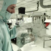
Researchers from Holst Centre have become the first to use spatial atomic layer deposition (sALD) to create both the semiconductor and dielectric layer in a thin-film transistor (TFT) backplane. Using a low-temperature, large-area process for the backplane, the team created a 200 ppi QVGA display demonstrator. The process allows TFTs to be produced on cheaper, transparent plastic foils, significantly reducing the cost of flexible electronics applications such as displays and image sensors. To showcase the technology, Holst Centre has produced a display demonstrator using a backplane of top-gated self-aligned TFTs on a PEN foil. The display is being presented at the International Display Workshop (IDW) in Sapporo, Japan from November 27-29.
|
The backplane was produced at temperatures below 200 °C, achieving mobilities of 8 cm2/Vs in transistors with channel lengths down to 1 μm. It was then combined with an OLED frontplane to create a 200 ppi QVGA display.
The demonstrator was produced using sALD equipment initially developed by Holst Centre and which is currently being commercialized by the start-up SALDtech. Spun out from Holst Centre in 2018, SALDtech offers the only sALD tools for Gen 1 (32 x 25 cm) substrate size flat-panel displays currently available. Earlier this year, it received a second round of investment to develop and build production equipment that could be integrated into the production lines of next-generation flexible OLED displays for mobile phones, tablets, TVs and more.
“We are already delivering TFT performance with sALD that is comparable with the best sputtered devices. And through additional optimization of processes and materials, there is considerable room for further improvements. At the same time, we are looking at producing all TFT layers with sALD to further simplify and reduce the cost of high-volume flexible TFT manufacturing,” says Ilias Katsouras, Senior Scientist at Holst Centre.
Many flat-panel displays today use the semiconductor indium gallium zinc oxide (IGZO) in the TFT backplane. IGZO is usually deposited via sputtering and requires a high-temperature anneal procedure to ensure performance. This high-temperature step necessitates substrates with high melting points, which are typically more expensive.

Developed by Holst Centre, large-area sALD is an atmospheric-pressure technique that allows ultra-thin layers of materials to be deposited quickly with high compositional control and excellent thickness uniformity. The technique has previously been used to produce high-quality individual layers of materials for solid-state batteries and TFT backplanes. Now, for the first time, Holst Centre has used sALD to deposit both the IGZO semiconductor layer and the aluminum dielectric-oxide dielectric layer in an integrated TFT process onto a low-cost, transparent plastic foil.
Using a single technique to produce multiple layers of material offers flexible TFT manufacturers the possibility of improving both production throughput and the interface between layers, which in turn increases device performance.
The demonstrator was produced using sALD equipment initially developed by Holst Centre and which is currently being commercialized by the start-up SALDtech. Spun out from Holst Centre in 2018, SALDtech offers the only sALD tools for Gen 1 (32 x 25 cm) substrate size flat-panel displays currently available. Earlier this year, it received a second round of investment to develop and build production equipment that could be integrated into the production lines of next-generation flexible OLED displays for mobile phones, tablets, TVs and more.
“We are already delivering TFT performance with sALD that is comparable with the best sputtered devices. And through additional optimization of processes and materials, there is considerable room for further improvements. At the same time, we are looking at producing all TFT layers with sALD to further simplify and reduce the cost of high-volume flexible TFT manufacturing,” says Ilias Katsouras, Senior Scientist at Holst Centre.
Many flat-panel displays today use the semiconductor indium gallium zinc oxide (IGZO) in the TFT backplane. IGZO is usually deposited via sputtering and requires a high-temperature anneal procedure to ensure performance. This high-temperature step necessitates substrates with high melting points, which are typically more expensive.

Developed by Holst Centre, large-area sALD is an atmospheric-pressure technique that allows ultra-thin layers of materials to be deposited quickly with high compositional control and excellent thickness uniformity. The technique has previously been used to produce high-quality individual layers of materials for solid-state batteries and TFT backplanes. Now, for the first time, Holst Centre has used sALD to deposit both the IGZO semiconductor layer and the aluminum dielectric-oxide dielectric layer in an integrated TFT process onto a low-cost, transparent plastic foil.
Using a single technique to produce multiple layers of material offers flexible TFT manufacturers the possibility of improving both production throughput and the interface between layers, which in turn increases device performance.


%20(1).png)

No comments:
Post a Comment