Thursday, October 17, 2019

The Nobel Prize in Chemistry 2019 - A highly competitive breeding ground for new IP

The motivation for this year's Nobel Prize in chemistry reads "for the development of lithium-ion batteries". John B. Goodenough (The University of Texas at Austin, USA), M. Stanley Whittingham (Binghamton University, State University of New York, USA) and Akira Yoshino (Asahi Kasei Corporation, Tokyo, Japan and Meijo University, Nagoya, Japan) receive the award as well as SEK 3 million each.

The basis for the lithium-ion battery was laid during the oil crisis in the 1970s. Lithium-ion batteries are light, rechargeable, and powerful batteries that are used in everything from mobile phones to laptops and electric vehicles (EVs). The lithium battery cells can also be deployed in systems to store vast amounts of energy produced by solar and wind power, which enables a fossil-free society.
The battery technology that has conquered the world

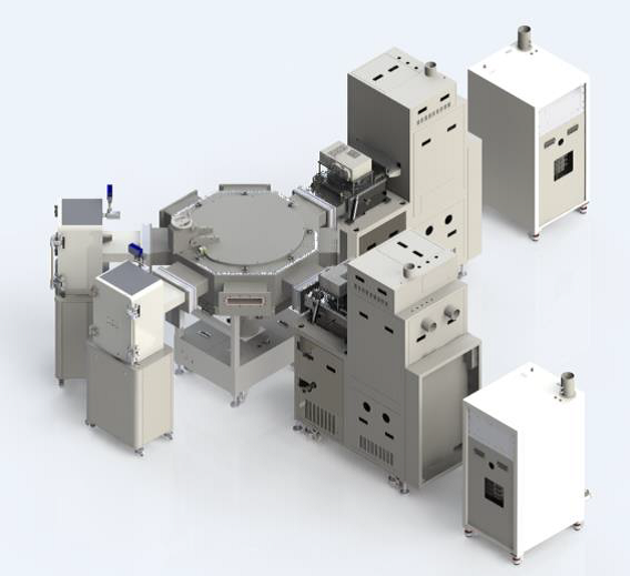
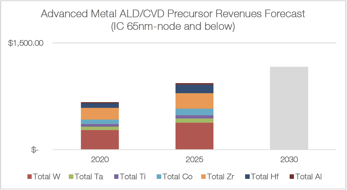
Since the first lithium-ion batteries came on the market in 1991, they have entirely changed the existence throughout the world. They have laid the foundation for a wireless and fossil-free society, and are today of enormous benefit to humanity. If we look at the lithium-ion battery from a technical and innovative perspective and link the technology area to patents, we see an explosive increase in patent applications between the years 2008-2017, a period when battery technology has penetrated the world market. Some of the large companies that have been inspired by the Nobel Prize winners and their technical achievements are: Tesla (USA), Toyota (Japan), Volkswagen (Germany), BASF (Germany), Umicore (Belgium), CATL (China) and Northvolt (Sweden), which is currently establishing itself in northern Sweden. These are companies active across the complete value chain, from raw materials suppliers, battery cell production to end-user consumer applications.

A minefield for new patent applications

The companies and innovators who are now entering the lithium-ion technology business and are considering applying for patents, no matter what application area they intend to work in, are entering a veritable minefield. It is an extremely challenging area for new patent applications. The situation places high demands on qualified analysis of both the main technology area, adjoining technology areas, market situations, the actions of existing players and new players' strategies. Here, adequate patent information in the hands of an expert in patent information can straighten out many question marks, not least because the patent data consists of both technical, legal, and business-related information.

To see what the others do not see

When I, as an expert in seeking, analyzing, and drawing conclusions from patent information, launches, both the historical, the current, and the future perspectives, are at stake. Drawing conclusions from historical patent data and translating it into future potential is an unusual ability that not many commands.

The amount of patent data, the variety of data, and the speed at which new patent data is published are continuously increasing. Properly handled and, above all, adequately analyzed, patent data can increase insights, support business decisions, and create new values and stronger negotiating positions for your company. I think it is a waste not to use the power of patent data more than is done today.

Contact me so we take a closer look at a technology area that is important to your company's future.

Ervin Dubaric


Guest Blog by Dr. Ervin Dubaric, Patent Information Specialist at Bergenstråhle & Partners, Stockholm, Sweden

Intel Oregon is looking for young CVD, ALD and PVD experts

[Intel, Hillsboro Oregon, USA] We are hiring Ph.D. candidates or recently received a Ph.D. degree in the metals thin-film area. We are giving priorities to the candidates who have exceptional backgrounds in physical vapor deposition (PVD), chemical vapor deposition (CVD), atomic layer deposition (ALD), and/or Electrodeposition fields. Strong plasma physics and vacuum science knowledge will be needed for PVD, CVD, and ALD deposition area candidates. 
 
 
 Intels Fab D1X in Oregon USA (Intel.com)
 
We are also looking for candidates with synthetic chemistry backgrounds for CVD/MOCVD (metal-organic chemical vapor deposition) precursor development. In the Electrodeposition area, we are looking for candidates with a strong background in electrochemistry, plating related thin film deposition.

Generic Job description can be found here - https://jobs.intel.com/ListJobs/ByKeyword/JR0099326/

Please send me your resume directly to shaestagir.chowdhury@intel.com
 
------------
Guest Blog by Dr. Shaestagir Chowdhury, Principal Engineer at Intel Corporation, Hillsboro, Oregon
 

Wednesday, October 16, 2019

What can Atomic Layer Deposition do for solar cells

Here is an excellent article by Pro. Kessels and Dr Bart from TU Eindhoven on the current status of Atomic Layer Deposition in the solar industry (Atomiclimits.com LINK).

ALD PV applications:

  • ALD for passivation layers and passivating contacts
  • ALD for transparent conductive oxides (TCOs)
  • ALD in the upcoming field of perovskites and tandem cells

Potential new applications for ALD in PV:


  • ALD Al2O3 for hydrogenation of poly-Si passivating contacts
  • ALD for hybrid metal halide perovskite and Si-perovskite tandems


Tuesday, October 15, 2019

Lund University Holding invests in newly started AlixLabs

LU Holding invests in newly started AlixLabs, which have developed a method to manufacture electronic circuits for the semiconductor industry in a very cost-effective way.

[Published on September 27, 2019: Original in Swedish: LINK]

Researchers from NanoLund have developed and patented the method and all three, Jonas Sundqvist, Dmitry Suyatin, and Sabbir Kahn, are part of the newly started company (AlixLabs AB), and Co-founder Stefan Svedberg joins as CEO. Svedberg was previously Director of Corporate Development at Ericsson.

Displaying the Edge Effect: This is a new method of nanostructure fabrication using the atomic layer etching process, which is inherently a damage-free etch process. The recently discovered etching process selectivity to inclined surfaces, can be used as a mask and in this way walls of tapered structures. The inclined surfaces can be readily fabricated by e.g. dry etching or epitaxial growth, and will provide masking during the atomic layer etching process. This process therefore provides access to fabrication of extremely small structures in a very precise and efficient way.

Electronic circuits are needed in all types of hardware, but the cost of producing them has increased as the electronics become smaller. With the AlixLab method, which is based on a recently identified physical phenomenon, the manufacturing process of the electronic circuits becomes both faster and significantly cheaper.

Dr. Dmitry Suyatin, Co-founder and CTO and Dr. Jonas Sundqvist, Co-founder and Senior Technical Adviser at AlixLabs inspecting the new Atomic Layer Etching Equipment at Lund Nano Lab from PlasmaTherm.
 
"AlixLabs has an exciting technology, and now we have a good team in place," says Erik Larsson, portfolio manager at LU Holding.

Alixlabs plans to implement an expanded proof of concept in 2020 as the basis for continued customer discussions.
AlixLabs Team : LINK

Short cources in ALD and ALE Jaunuary 14-15 in Eindhoven (NL)

On January 14-15 the ALD Academy will organize some courses on ALD and ALE (=Atomic Layer Etching) in Eindhoven, The Netherlands. You can register per individual course. See the website for more details.

LINK: https://www.aldacademy.com/ald-and-ale-courses/

High device performance of unique ALD-IGZO TFTs to look forward to expanding application area to semiconductor

Amorphous In-Ga-Zn-O (IGZO) materials have been mainly employed as channel materials for the backplane TFTs of flat panel displays (FPDs) owing to their superior characteristics of excellent uniformity, high on/off current ratio, and superior carrier mobility to other amorphous oxide semiconductors. Recently, IGZO thin films have been actively researched for high-end future electronic applications such as TFTs of DRAM and NAND which are typical semiconductor memory devices as well as transparent flexible displays, sensors and logic architectures.

Especially, considering indispensable three dimension architectures of the memory devices for high functional AI semiconductors, the interest in application of IGZO TFTs has been rapidly increased because they are satisfied with the requirement of low power consumption and low operation temperature.

The atomic layer deposition (ALD) method is resulting in better film quality even at a lower deposition temperature. Furthermore, the film thickness and composition can always be precisely controlled at the atomic scale with excellent conformality and higher film density. However, ALD process for IGZO as multi-component materials has the difficulty of control between metal precursors and oxidants.


Variations in transfer curves with the lapse of stress time for 104 s under PB(T)S conditions for Dev. (a) A(1:1:1) and B(1:1:3) at RT and for Dev. (c) A and (d) B at 60℃. (VGS= +20V, VDS= 10.5 V)*


The targeted atomic compositions (In:Ga:Zn) of ALD-IGZO films were acquired by controlling the ALD cycle ratios using the unique ALD method to clear this issue. The device employing (1:1:3) composition exhibited the most desirable characteristics from the viewpoint of excellent bias stability, and they were found to be superior to those by the conventional sputtered-deposited IGZO TFTs.

Therefore, this method to control the compositions of IGZO could be a core technology to guarantee high performance and robust stability for various future ALD-IGZO thin film applications.


Si wafer based batch ALD cluster system

NCD has been developing high throughput batch ALD-IGZO system using the unique technology capable of controlling the designed atomic compositions of IGZO for etch applications. This system could provide the excellent quality competiveness and functional stability as well as high throughput in production of 3D complex architectures such as future Logic, DRAM and NAND devices expected to apply ALD-IGZO thin films.

*Journal of Materials Chemistry C, 2019, 7, 6059, Cationic compositional effects on the bias-stress stabilities of thin film transistors using In-Ga-Zn-O channels prepared by atomic layer deposition, Seung-Bo Ko, Nak-Jin Seong, Kyujeong Choi, So-Jung Yoon, Se-Na Choi, and Sung-Min Yoon. DOI: 10.1039/c9tc01164a

Link : http://www.ncdtech.co.kr/2018/bbs/board.php?bo_table=eng_board_05&wr_id=45

Friday, October 4, 2019

Global Market Remains Strong for ALD & CVD Precursors in IC Fabs

San Diego, CA, October 2, 2019: TECHCET—the advisory services firm providing electronic materials information— announced that the global market for atomic layerdeposition (ALD) and chemical vapor deposition (CVD) precursors is showing strong
growth despite semiconductor fabrication market challenges in 2019. CVD growth is mainly in plasma-enhanced CVD (PECVD) and metal-organic CVD (MOCVD) for silicon ICs and for newer devices including micro-displays, RF for 5G, and photonics. The
combined ALD and CVD metal precursor market is estimated to be approximately US$582M in 2019 growing 6.3% from the prior year and forecasted to grow above US$930M by 2025, as detailed in the latest Critical Materials Report™ (CMR) on ALD /
High-K Metal Precursors (see Figure).

Advanced Metal ALD/CVD Precursor Revenues Forecast
“Today, the top three suppliers ADEKA, Air Liquide, and Versum dominate the market by controlling ~75% of the segments,” explained Dr. Jonas Sundqvist, TECHCET senior technology analyst and author of the report. “However, due to the recent development that Merck will acquire Versum, there is a good chance that by doing so it will become the number one supplier for all type of metal, High-κ, and dielectric precursors.” The CVD, ALD, and SOD market includes from both specialty gases (e.g. WF6) and liquid precursors, as well as a considerable segment of solid precursors (e.g. HfCl4, PDMAT). In addition, there are smaller segments for precursors that still do not reach annual sales of >US$5 million such as ruthenium and rare earth elements (REE).
This report covers the following suppliers: ADEKA, Air Liquide, Air Products, AZmax Co., BASF, DNF Co., Entegris, Epivalence, FujiFilm, Gelest, Hansol Chemical, H.C.Starck, Kojundo, Linde (Praxair), Mecaro, Merck EMD, Nanmat, Norquay, Pegasus
Chemicals, Soulbrain, Strem, Tanaka Kikinzoku Group, Tokyo Chemical Industry Co.,Tri Chemical Laboratories, Umicore, UP Chemical (Yoke), and Versum.

Purchase ALD/CVD Reports Here: TECHCET Reports

Wednesday, September 25, 2019

Device Engineer at Petabyte in Shanghai for FRAM Cell/Array engineering


Job Description

This position is for a Device/Testing Engineer working on FRAM Cell/Array engineering. The engineer is responsible for leading research and development of next generation VFRAM to support Petabyte Technology Inc’s (PBT) growing business in storage and memory solutions. Primary responsibilities include silicon experimentation, cell and array characterization, data analysis, modelling of the device, array, circuits and system behavior to meet complete product requirements and system needs. The engineer is also responsible for developing innovative device solutions and memory operation algorithms to continue technology scaling. Successful candidate will collaborate with process integration engineers, circuit designers, product engineers to understand the critical issues and inter-dependencies and engineer solutions to address them.

Location: Shanghai, China
Traveling: <20%
Salary: TBD
Language: English/Chinese

Qualifications

Education:Candidate should possess an MS degree with at least 4 years additional experience, or a PhD with at least 2 years additional experience, in Electrical Engineering or Physics, with an emphasis in Physics of Semiconductor Materials or Devices/Testing related areas.

Hands on experience with FRAM/FEFET in device and testing are strongly preferred!!

Bench testing experience is preferred but not required.

Device modeling is preferred but no required.

Minimum Requirements:
- 4+ years' experience in the area of Semiconductor and Device Physics, or device processing, electrical characterization, and device and circuit models.
- 4+ years' experience in technical problem solving.

About PBT

Petabyte Technologies is a high-tech enterprise focusing on the R&D and sales of new memory chip - FRAM, a new kind of NVM(Non-Volatile Memory). The project team brings together the world's top experts in memory development, with an average of more than 15 years of cutting-edge technology experience.

The FRAM technology, Petabyte’s proprietary intellectual property, adopts brand new material and architecture. The FRAM memory is designed to fill the gap between the two main stream memories, DRAM and Flash. It is equipped with fast read-write speed, accurate addressing to byte, high durability, flash-like non-volatility and low power consumption. Petabyte’s FRAM can immensely increase storage density current memories.

FRAM has a wide application such as future smart market (including household, office, instrumentation, automotive electronics) and AI chips market.

About Our Group

The Cell development Group is responsible for delivering new memory Cell solutions to PBT’s (Petabyte Technology. Inc) most advanced memory products. As part of the cell development team, we develop the best-in-class materials solutions and partner with process integration, product and Design teams to introduce these solutions into new memory products. As an enabler of head performance and reliability advances through cell innovation, we help PBT lead in technology and time-to-market.

Contact:

Sharon Yin

E-mail: xryin@petabytetech.com

Mobile:(+86)18914135998

Wechat:13921177520


Beneq unveils Transform(TM), a versatile automated ALD platform for More-than-Moore device fabrication

Combination of thermal and plasma ALD, single wafer or batch processing, and a unique preheating module maximize options for flexible volume production

25 September, 2019, Grenoble, France – Beneq, a leading provider of ALD R&D and production technology, today announced the BENEQ TransformTM, a versatile ALD platform dedicated to More-than-Moore device fabrication.


The brand-new cluster design offers customers unparalleled flexibility by combining both thermal and plasma ALD with single wafer and batch processing, on a single automated platform. Fully compliant with industry quality and SEMI standards the BENEQ TransformTM is a one-stop ALD solution for Power Electronics, MEMS and Sensors, RF, LED, Photonics, and Advanced Packaging applications.

“Among hundreds of application requests brought to us by customers today, we are most excited by GaN devices for RF and Power applications as well as Photonics, both III-V and Silicon,” said Dr. Patrick Rabinzohn, Beneq’s Semiconductor Business Executive. “In particular surface passivation, gate dielectrics, nucleation layers and encapsulation layers are all well addressed with the BENEQ TransformTM.”

Truly Versatile


More than Moore (MtM) applications are evolving at a phenomenal pace. To be competitive manufacturers are adopting advanced thin film technologies. Often, they need to combine surface preparation, interfacial layer and functional layer deposition sequences - all in one tool.

Currently available ALD production systems offer only one type of ALD process - either thermal or plasma enhanced. This creates the need for a versatile tool that supports multiple deposition capabilities.

The BENEQ TransformTM confidently combines thermal and plasma ALD processing, on a single wafer or in batches, while easily configurable. It is capable of surface pre-treatment and can coat substrate materials at wafer sizes from 3 to 8 inches.

It works well for R&D, prototyping, as well as volume production. With the BENEQ TransformTM customers now have the option to run several different ALD processes on multiple devices and applications, all on a single footprint!

The most complete configuration offers two ALD process modules, pre-heating station, surface plasma treatment and wafer cooling.

Designed for the Fab


Unlike ALD production platforms featuring vertical flip functions, the TransformTM loads wafers in a horizontal position and seamlessly integrates with the rest of your production line. Such a loading mechanism is also proven to minimize handling issues, and particle generation associated with non-standard cassette batch loading systems.

The BENEQ TransformTM features a proprietary preheating module that eliminates hours of waiting time and boosts throughput to a whole new level (15 wph @50 nm Al2O3, in thermal mode). Throughput can be further increased by adding up to 2 more process modules, thermal or plasma.

The BENEQ TransformTM produces a wide range of oxides including Al2O3, HfO2, Ta2O5, TiO2, and SiO2, and nitrides such as AIN and TiN. What sets the TransformTM apart from other tools is its ability to scale up throughput and maintain the same uniformity regardless of the temperature, e.g. >400°C.

SEMI Certified


The BENEQ TransformTM shortens cycle time and speeds up fab adaptation by implementing SECS/GEM standards. It is fully compliant with SEMI S2/S8 for environmental, ergonomics and safe operations.

To learn more, visit www.beneq.com/transform.

About Beneq

Beneq is the home of ALD, offering a wide portfolio of equipment products and development services. Today Beneq leads the market with innovative solutions for flexible high-volume manufacturing (BENEQ TransformTM), advanced R&D (TFS 200, R2), ultra-fast high precision spatial ALD coatings (C2R), roll-to-roll thin film coating of continuous webs (WCS 600), and specialized batch production for thicker film stacks (P400, P800). Headquartered in Espoo, Finland Beneq is dedicated to making ALD technology accessible for researchers and providing the invisible advantage in emerging semiconductor applications.

Press Contact
Lie Luo
Beneq
lie.luo@beneq.com