Tuesday, May 12, 2015

Argonne chooses Beneq’s TFS 500 Atomic Layer Deposition System

Argonne chooses Beneq’s TFS 500 Atomic Layer Deposition System. It all started with learning about Beneq’s range of atomic layer deposition (ALD) equipment at conferences. Once Argonne National Laboratory, the largest national laboratory by size and scope in the US Midwest, began looking into the systems in more detail, it became clear that Beneq was a natural choice for their ALD research needs. The Beneq TFS 500 system has offered exceptional modularity and flexibility, allowing Argonne to continue driving breakthroughs in energy technology.

A natural choice
“It was the nature of Beneq’s business approach, and the way they closely connect to the needs of researchers,” describes Dr Jeffrey Elam, Principal Chemist and Group Leader at Argonne National Laboratory outside of Chicago.

“We were really impressed. Beneq doesn’t just sell a tool or a piece of equipment. Instead, the company aims to innovate a solution by truly understanding the work that we do. To meet our specific needs, they worked very closely with us. That’s why the company was a natural choice for us,” Jeff continues.

Using technology to change the world
Argonne’s mission is to pursue big, ambitious ideas that redefine what is possible. A “dream team” of world-class researchers, including Jeff, work to solve large challenges, such as clean energy, where his team is now focused. The goal is to develop useful technologies that can transform the world.

To achieve technological breakthroughs, Argonne offers its researchers scientific facilities with a range of cutting-edge tools. As founder of Argonne’s ALD program, Jeff focuses on the R&D of novel thin film coating technologies from inception to commercialization.

Modularity – the only way
Argonne has been using Beneq’s TFS 500 for numerous projects over the last five years, including the development of large-area photo detectors. For this particular project, Argonne needed to coat large substrates with a high degree of internal porosity while maintaining excellent uniformity in both thickness and composition – a formidable coating challenge.


Beneq’s TFS 500 is a hands-on ALD tool for multi-project environments. Built for researchers by researchers.

As Jeff explains: “Beneq has long experience with ALD that reaches back to the invention of this deposition technique by Dr Tuomo Suntola and co-workers. As a consequence, Beneq is exceptional at designing tools. When we started the photodetector project, our own process was not yet well defined. As we experimented with different ALD chemistries and coating strategies, we needed a tool that was flexible and easily adapted to evaluate our ideas,” he describes. “One of the main advantages is that Beneq’s system is modular. There really was no other way for us to do this work.”

So far, Beneq’s TFS 500 has been operating really well for the past five years. “We can use it with any development project since it’s easy to reconfigure. For instance, we can install the small, 200 mm reaction chamber to test out new chemistries using only minimal amounts of precursor. Alternatively, we can connect our large 3D reaction chamber and coat batches of 300 mm wafers to investigate the process at a pilot scale. This flexibility is really unique to Beneq.”


Beneq TFS 500 with multi-purpose batch reaction chamber installed.


“We frequently encounter unexpected challenges when scaling ALD processes from small to large substrates,” Elam says. “The modularity of the TFS 500 system allows us to easily reconfigure the tool, and this speeds up our development and enables us to overcome these challenges.”

A perfect trio: researchers, Beneq and industry
Innovations in thin film technology go hand-in-hand with developments in the coating tools, as Jeff points out. “I think the best team for developing ALD technology in new areas combines researchers, tool manufacturers, and the companies that become the end-users of the technology. In this respect, we know we’ve got a winning combination with Beneq,” he continues. “They know how to appeal to researchers and also to work with companies that need to keep their production costs low. Beneq strikes a perfect balance with this,” he says.


Beneq offers the TFS 500 with a great variety in substrate configurations, interchangeable reaction chambers and more, all designed to enable top quality processes.

“Our ultimate aim is to pass our solutions on to companies who can commercialize them and so have a positive impact on the world. We’ve recently licensed our ALD-based detector technology to Incom, Inc. in Charlton, Massachusetts. Beneq worked with Incom to deliver a TFS 500 to their facility that would duplicate the process we developed here at Argonne on our tool. Now they can take our work forward and make it a business success. It’s a really nice three-way collaboration story,” Jeff smiles.

Versatile research tool
“Much of our work at Argonne centers around energy – solar cells, batteries, and catalysts for biofuels,” Elam says. “And we’ve got quite a lot of different projects going on in our laboratories at the same time.”

The versatility of Beneq’s TFS 500 is well matched for this diverse research environment. “The system works really well over a broad range of temperatures, chemical precursors, operating conditions, and substrate types,” Jeff notes. “With this flexibility, we can quickly set up the tool to handle multiple projects, even in the same day. This allows us to keep on top of our programs and collaborations.”

The future of ALD technology
The commercialization of ALD technology has been extremely successful in microelectronics, where ALD coatings can be now found in virtually any piece of consumer electronics. “The challenge now,” Elam notes, “is to duplicate this success in other industries. There are many examples in the literature demonstrating that ALD coatings can improve the performance of solar cells, organic LEDs, catalysts, lithium batteries, and more. Which of these applications succeed will come down to economics,” Jeff explains. “Most of them are still far from commercial reality. It’s not enough to be better – it also has to be affordable.”

“This is an exciting time to be involved in ALD research,” Jeff says. “Many of these new applications will require ALD coatings on large, porous substrates, and this will have to be done fast and cheap. New ALD processes must be developed, and new coating tools will need to be designed,” he notes. “I think Beneq is in a position to play a key role in the success of these new applications for ALD in energy technology.”

For more information about ALD, Beneq and the TFS 500, please contact:
Mr Pasi Meriläinen
Head of Research Equipment, Beneq
Tel: +358 40 510 3004
e-mail: pasi.merilainen(at)beneq.com

Read this news in PDF-format

Monday, May 11, 2015

New ALD Startup company from Harvard - Anric Technologies

As a new startup company from Boston - Anric Technologies introduces the AT-400. ALD equipment and processes developed from the ground up with three major design goals: ease of use, reproducibility and value.  the AT-400 ALD system is the first product of this design philosophy (www.anrictechnologies.com)


Acording to information at their Japanese representation most of us will identify to famous ALD personalities without any knowledge in Japanese (http://aldjapan.com/) - so I assume Prof. Roy Gordon and Philippe de Rouffignac are both involved in this new start up - I will update as soon as I find more infromation:
開発者の紹介
Philippe de Rouffignac, Ph.D は現在Harvard University, Department of Chemistry (Dr. Roy Gordon)、及びCenter for Nanoscale Systems でCVD/ALD のプレカーサなどの開発を担当。
学生時代もDr. Gordon の元で5台のALDを手作りし、メーカー勤務時代もALD開発に従事。


Basic Facts
  • Up to 4” diameter sample
  • Chamber temperatures from RT to 350 °C ± 1 °C
  • Precursor temperatures from RT to 150 °C ± 2 °C with optional heating jackets
  • Variable process pressure control 0.1 to 1.5 torr
  • All metal sealed system upstream of sample
    • No atmospheric contaminants at sample
  • Smallest footprint on market, cleanroom compatible
  • Precise precursor dosing with defined dose volumes
    • Reduces process and dose variability common to competitors
  • Fast cycling capability
    • 6-10 cycles/min or up to 1.2nm/min Al2O3 (best in class)
    • Exposure control for deposition on high aspect ratio samples
  • Robust touchscreen PLC control system
    • roven recipes pre-loaded in controller
  • Simple system maintenance and integrated vacuum interlock
  • User defined sample fixturing available
  • Streamlined chamber design and small chamber volume
    • Designed for high quality growth on small samples
     
  • 3 organometallic sources - standard 
    • All three can be heated up to 150 degrees C
    • Our inert gas pressure assist (IGPA) is an option for ultra low vapor pressure precursors
    • 2 counter reactants - standard
    • 1 liquid source such as H2O or H2O
    • 1 gas source such as O2 or NH3
    • 2 gas sources can be used as well

  •  

Saturday, May 9, 2015

ALD Technology on top by PV Magazine - The 2nd ALD Boom?

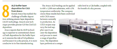
ALD equipment manufacturing technologies came in on top in the 50 Technology Highlight report by PV Magazine as published in the 2015 April issue. Both SoLayTec (#2) and AVACO (#8) made the top 10.


Not only did these two ALD companies make it to this honorable list they also made some major progress business wise. So the question is now will 2015 be like 2005 when ALD made it in to high volume manufacturing for a commodity product in the Semiconductor Industry at the introduction of high-k dielectrics for the DRAM memory cell capacitors - The 2nd ALD BOOM!

"Mr. Fokko Pentinga, Chief Executive Officer of Amtech, commented, 'We made much progress in the quarter including the successful close of the BTU acquisition and the integration of both BTU and SoLayTec is progressing according to plan. Bookings continued at a healthy rate in the quarter and our backlog is at the highest level in the last three years. The mix of product in our backlog, including PECVD, ion implant, and atomic layer deposition systems (ALD), is a direct result of our decision several years ago to invest in expanding the size of our served available markets through product development and acquisition. Global solar installations continue to grow and the balance between supply and demand continues to improve. With strong growth of the market in 2015 and beyond, we see an increase in activity among top tier solar cell manufacturers to expand production both inside and outside of China and we are pleased to fully participate in the industry's selective capacity expansion and technology adaptation.'"


According to earlier reports in April "AVACO received additional volume order for PV manufacturing line that will be installed in China from one of the major solar manufacturer in the U.S. AVACO specializes in the manufacturing sputtering (PVD) vacuum deposition equipment, SuVAS™, and atomic Layer deposition (ALD) equipment AEON™. With the expertise in providing the turnkey manufacturing solution, AVACO boosts the PV market momentum."


Friday, May 8, 2015

Picosun - The ALD Company


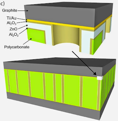
Polycarbonate nanocomposite ALD coated device for measuring thermal conductivity in thin films

As reported by Nanotech.org : The thermal conductivity of thin films can differ drastically from that of bulk samples. With thin material layers increasingly being used in microelectronic and optoelectronic components, measurement techniques for determining the thermal conductivity are desirable. Additionally, the potential to tune the thermal conductivity is interesting for applications within the field of energy production. Reporting in Nanotechnology, Finnish and Norwegian researchers determine the in-plane thermal conductivity of thin films using the laser flash method. The work allows for the study of thin films using standard measurement equipment that is available in many research facilities.


Researchers at Aalto University and the University of Oslo use atomic layer deposition (ALD) to create a well-defined nanocomposite. This can be measured using the laser flash method. 

Continue reading here.

MIT Engineers Repair Graphene Water Filters by ALD

Here is an interesting story from Engineering.com on "How Engineers Repaired One-Atom Thick Graphene Filters"

(Image courtesy MIT News)

Graphene seems to be the next big thing in water filtration as scientists look to create ultrathin membranes to filter out contaminants. Only problem is, defects in the making of one-atom thick membranes are a common occurrence, causing leaks.


In a two-step process, engineers have successfully sealed leaks in graphene. First, the team fabricated graphene on a copper surface (top left) — a process that can create intrinsic defects in graphene, shown as cracks on the surface. After lifting the graphene and depositing it on a porous surface (top right), the transfer creates further holes and tears. In a first step (bottom left), the team used atomic layer deposition to deposit hafnium (in gray) to seal intrinsic cracks, then plugged the remaining holes (bottom left) with nylon (in red), via interfacial polymerization. (MIT News)

Hope is not lost though as engineers have found a way to repair the cracks and holes, filling them with a combination of chemical deposition and polymerization techniques.

The first of the two techniques used, addresses the smaller intrinsic defects. Using a process called “atomic layer disposition,” the team placed the graphene membrane in a vacuum chamber, pulsing in a hafnium containing chemical that normal does not interact with graphene.

In this scenario the chemical sticks to openings in the graphene, attracted to the area’s higher surface energy.

After several rounds of applied atomic layer deposition, the hafnium oxide successfully filled in the graphene’s nanometer-scale intrinsic defects.

This solution quickly unveiled a new issue, as the team realized it would require too much time to fill in the membranes larger defects. 
 

Thursday, May 7, 2015

Atomic Layer Deposition: Russia, 2015 Sept 21

The Russian ALD 2015 Workshop will be organised 21—24 September 2015 in Moscow. More information will be published here as they come in (Thanks Riikka!)

The workshop is organised by Moscow Institute of Physics and Technology, State University.

Bildergebnis für moscow institute of physics and technology

To follow on Twitter you should use : #RussiaALD 
"Atomic Layer Deposition (ALD) is a thin film coating technique, which has gradually manifested itself as a powerful tool to fabricate ultrathin, highly uniform and conformal material layers for many applications. The idea of the Workshop “Atomic Layer Deposition: Russia, 2015” is to consolidate the rapidly growing Russian ALD community, and to bring closer Russian researchers to the leading international experts in the field."

As I have posted earlier I do recently see a tremendous increase in traffic from Russia to this blog. last month Russian visitors made it up to 2nd place after the U.S. visitors:

EntryPage views
United States
2048
Russia
769
Ukraine
653
France
473
Sweden
387
Germany
343
Japan
255
Finland
206
Netherlands
105
United Kingdom
66

Wednesday, May 6, 2015

Cu-TiOx -TiNx NIS tunnel junction with ALD BENEQ TFS-200 TiN as Superconductor

My favourite ALD film is suddenly superconducting! Cu-TiOx -TiNx NIS tunnel junction with ALD BENEQ TFS-200 TiN as Superconductor from Department of Physics, University of Jyvaskyla,  Finland. Full manuscript available here thru the following link: https://jyx.jyu.fi/dspace/handle/123456789/45757


Normal-Metal–Insulator–Superconductor Tunnel Junction With Atomic-Layer-Deposited Titanium Nitride as Superconductor


Andrii Torgovkin, Saumyadip Chaudhuri, Jari Malm, Timo Sajavaara, and Ilari J. Maasilta
10.1109/TASC.2014.2383914

We report the fabrication of 70–350-nm-thick superconducting titanium nitride (TiNx) films using the atomic layer deposition (ALD) technique and the subsequent fabrication of normal metal–insulator–superconductor (NIS) tunnel junction devices from the ALD films. The films were deposited on a variety of substrates: silicon, silicon nitride, sapphire, and magnesium oxide. Superconductivity, with transition temperatures ranging from 1.35 to 1.89 K, was observed in all films. was found to depend on both the substrate type as well as film thickness. Cu-TiOx -TiNx NIS tunnel junction devices were fabricated from the TiN film deposited on silicon, using electron beam lithography and shadow angle evaporation techniques. These devices exhibit temperature-dependent current–voltage characteristics and good thermometric response from 0.1 K to slightly above . Nonlinearity in the current–voltage characteristics was observed even at temperatures as high as 5 , indicating the presence of a pseudogap in these TiNx films.


ALD oxides used in vertical gallium nitride MOSFETs with reduce on-resistance

As reported by Semiconductor Today: Toyoda Gosei Co Ltd in Japan has developed a vertical trench metal-oxide-semiconductor field-effect transistor (MOSFET) on free-standing gallium nitride (GaN) combining 1.2kV blocking voltage with low specific on-resistance [Tohru Oka et al, Appl. Phys. Express, vol8, p054101, 2015]. The researchers comment: "To the best of our knowledge, this is the first report on vertical GaN-based MOSFETs with a specific on-resistance of less than 2mΩ-cm2." 

Interestingly the integration employs a 80 nm ALD SiO2gate dielectric and a100 nm ALD Al2O3 800 nm PECVD SiO2 combo interdielectric. This basically shows two things:

1) Oxides by ALD is not all about high-k
2) ALD is also used for relatively thick layers and not only 10 to 100 Å in microelectronics


Figure 1

Transistor fabrication (Figure 1) involved inductively couple plasma (ICP) etching for mesa isolation, p-body contact recessing, and gate trenching. The gate dielectric was 80nm silicon dioxide, grown using atomic layer deposition (ALD). Interlayer dielectrics of 100nm aluminium oxide and 800nm silicon dioxide were produced by atomic layer deposition and plasma-enhanced chemical vapor deposition (PECVD)(Picture from Semiconductor Today).


Tuesday, May 5, 2015

Annealsys Workshop from RTP to RTCVD and CVD to ALD May 13 E-MRS Spring meeting in Lille


Annealsys Workshop from RTP to RTCVD and CVD to ALD. Wednesday May 13 at 9h30 held during the E-MRS Spring meeting in Lille


  • Learn more about our solutions for RTP and RTCVD and our multi process capability RTP machines up to 2000°C.
  • Learn more about our solutions for CVD and ALD and our multi process capability DLI-CVD / DLI-ALD systems
See invitation!

Monday, May 4, 2015

2D Molybdenum disulfide encapsulated between layers of boron nitride

Beautiful work of 2D material stacks for future electronics - layered stacks of molybdenum disulfide (MoS2) encapsulated in boron nitride (BN), with graphene overlapping the edge of the MoS2 to act as electrical contacts as Published by : Holly Evarts, "Two-Dimensional Semiconductor Comes Clean", Apr. 27, 2015 and in Nature Nanotechnology below.
Bookmark and Share 

In 2013 James Hone, Wang Fong-Jen Professor of Mechanical Engineering at Columbia Engineering, and colleagues at Columbia demonstrated that they could dramatically improve the performance of graphene—highly conducting two-dimensional (2D) carbon—by encapsulating it in boron nitride (BN), an insulating material with a similar layered structure. In work published this week in the Advance Online Publication on Nature Nanotechnology’s website, researchers at Columbia Engineering, Harvard, Cornell, University of Minnesota, Yonsei University in Korea, Danish Technical University, and the Japanese National Institute of Materials Science have shown that the performance of another 2D material—molybdenum disulfide (MoS2)—can be similarly improved by BN-encapsulation.


Two-dimensional semiconductor comes clean 

Schematic cross-section view of atomic layer of molybdenum disulfide contacted by graphene, and encapsulated between layers of insulating hexagonal boron nitride. Credit: Gwan-Hyoung Lee/Columbia Engineering

Read more at: http://phys.org/news/2015-04-two-dimensional-semiconductor.html#jCp
Molybdenum disulfide encapsulated between layers of boron nitride (Image courtesy of Gwan-Hyoung Lee/Yonsei University).
Schematic cross-section view of atomic layer of molybdenum disulfide contacted by graphene, and encapsulated between layers of insulating hexagonal boron nitride. Credit: Gwan-Hyoung Lee/Columbia Engineering

Read more at: http://phys.org/news/2015-04-two-dimensional-semiconductor.html#jCp
Schematic cross-section view of atomic layer of molybdenum disulfide contacted by graphene, and encapsulated between layers of insulating hexagonal boron nitride. Credit: Gwan-Hyoung Lee/Columbia Engineering

Read more at: http://phys.org/news/2015-04-two-dimensional-semiconductor.html#jCp
Schematic cross-section view of atomic layer of molybdenum disulfide contacted by graphene, and encapsulated between layers of insulating hexagonal boron nitride. Credit: Gwan-Hyoung Lee/Columbia Engineering

Read more at: http://phys.org/news/2015-04-two-dimensional-semiconductor.html#jCp

Schematic cross-section view of atomic layer of molybdenum disulfide contacted by graphene, and encapsulated between layers of insulating hexagonal boron nitride. Credit: Gwan-Hyoung Lee/Columbia Engineering

“These findings provide a demonstration of how to study all 2D materials,” says Hone, leader of this new study and director of Columbia’s NSF-funded Materials Research Science and Engineering Center. “Our combination of BN and graphene electrodes is like a ‘socket’ into which we can place many other materials and study them in an extremely clean environment to understand their true properties and potential. This holds great promise for a broad range of applications including high-performance electronics, detection and emission of light, and chemical/bio-sensing.”

Two-dimensional (2D) materials created by “peeling’” atomically thin layers from bulk crystals are extremely stretchable, optically transparent, and can be combined with each other and with conventional electronics in entirely new ways. But these materials—in which all atoms are at the surface—are by their nature extremely sensitive to their environment, and their performance often falls far short of theoretical limits due to contamination and trapped charges in surrounding insulating layers. The BN-encapsulated graphene that Hone’s group produced last year has 50× improved electronic mobility—an important measure of electronic performance—and lower disorder that enables the study of rich new phenomena at low temperature and high magnetic fields.

“We wanted to see what we could do with MoS2—it’s the best-studied 2D semiconductor, and, unlike graphene, it can form a transistor that can be switched fully ‘off’, a property crucial for digital circuits,” notes Gwan-Hyoung Lee, co-lead author on the paper and assistant professor of materials science at Yonsei. In the past, MoS2 devices made on common insulating substrates such as silicon dioxide have shown mobility that falls below theoretical predictions, varies from sample to sample, and remains low upon cooling to low temperatures, all indications of a disordered material. Researchers have not known whether the disorder was due to the substrate, as in the case of graphene, or due to imperfections in the material itself.

In the new work, Hone’s team created heterostructures, or layered stacks, of MoS2 encapsulated in BN, with small flakes of graphene overlapping the edge of the MoS2 to act as electrical contacts. They found that the room-temperature mobility was improved by a factor of about 2, approaching the intrinsic limit. Upon cooling to low temperature, the mobility increased dramatically, reaching values 5-50× that those measured previously (depending on the number of atomic layers). As a further sign of low disorder, these high-mobility samples also showed strong oscillations in resistance with magnetic field, which had not been previously seen in any 2D semiconductor.

“This new device structure enables us to study quantum transport behavior in this material at low temperature for the first time,” added Columbia Engineering PhD student Xu Cui, the first author of the paper.

By analyzing the low-temperature resistance and quantum oscillations, the team was able to conclude that the main source of disorder remains contamination at the interfaces, indicating that further improvements are possible.

“This work motivates us to further improve our device assembly techniques, since we have not yet reached the intrinsic limit for this material,” Hone says. “With further progress, we hope to establish 2D semiconductors as a new family of electronic materials that rival the performance of conventional semiconductor heterostructures—but are created using scotch tape on a lab-bench instead of expensive high-vacuum systems.”

Multi-terminal transport measurements of MoS2 using a van der Waals heterostructure device platform
Xu Cui, Gwan-Hyoung Lee, Young Duck Kim, Ghidewon Arefe, Pinshane Y. Huang, Chul-Ho Lee, Daniel A. Chenet, Xian Zhang, Lei Wang, Fan Ye, Filippo Pizzocchero, Bjarke S. Jessen, Kenji Watanabe, Takashi Taniguchi, David A. Muller, Tony Low, Philip Kim & James Hone
Nature Nanotechnology(2015)doi:10.1038/nnano.2015.70
Schematic cross-section view of atomic layer of molybdenum disulfide contacted by graphene, and encapsulated between layers of insulating hexagonal boron nitride. Credit: Gwan-Hyoung Lee/Columbia Engineering

Read more at: http://phys.org/news/2015-04-two-dimensional-semiconductor.html#jCp
Schematic cross-section view of atomic layer of molybdenum disulfide contacted by graphene, and encapsulated between layers of insulating hexagonal boron nitride. Credit: Gwan-Hyoung Lee/Columbia Engineering

Read more at: http://phys.org/news/2015-04-two-dimensional-semiconductor.html#jCp
Schematic cross-section view of atomic layer of molybdenum disulfide contacted by graphene, and encapsulated between layers of insulating hexagonal boron nitride. Credit: Gwan-Hyoung Lee/Columbia Engineering

Read more at: http://phys.org/news/2015-04-two-dimensional-semiconductor.html#jCp
Schematic cross-section view of atomic layer of molybdenum disulfide contacted by graphene, and encapsulated between layers of insulating hexagonal boron nitride. Credit: Gwan-Hyoung Lee/Columbia Engineering

Read more at: http://phys.org/news/2015-04-two-dimensional-semiconductor.html#jCp
Schematic cross-section view of atomic layer of molybdenum disulfide contacted by graphene, and encapsulated between layers of insulating hexagonal boron nitride. Credit: Gwan-Hyoung Lee/Columbia Engineering

Read more at: http://phys.org/news/2015-04-two-dimensional-semiconductor.html#jCp


Figure 1c: Cross-sectional STEM image of the fabricated device. The zoom-in false-colour image clearly shows the ultra-sharp interfaces between different layers (graphene, 5L; MoS2, 3L;top hBN, 8nm; bottom hBN, 19 nm) [Figure and Abstract used with permission from Nature Publishing Group under License Number 3621820766388]

Atomically thin two-dimensional semiconductors such as MoS2 hold great promise for electrical, optical and mechanical devices and display novel physical phenomena. However, the electron mobility of mono- and few-layer MoS2 has so far been substantially below theoretically predicted limits, which has hampered efforts to observe its intrinsic quantum transport behaviours. Potential sources of disorder and scattering include defects such as sulphur vacancies in the MoS2 itself as well as extrinsic sources such as charged impurities and remote optical phonons from oxide dielectrics. To reduce extrinsic scattering, we have developed here a van der Waals heterostructure device platform where MoS2 layers are fully encapsulated within hexagonal boron nitride and electrically contacted in a multi-terminal geometry using gate-tunable graphene electrodes. Magneto-transport measurements show dramatic improvements in performance, including a record-high Hall mobility reaching 34,000 cm2 V–1 s–1 for six-layer MoS2 at low temperature, confirming that low-temperature performance in previous studies was limited by extrinsic interfacial impurities rather than bulk defects in the MoS2. We also observed Shubnikov–de Haas oscillations in high-mobility monolayer and few-layer MoS2. Modelling of potential scattering sources and quantum lifetime analysis indicate that a combination of short-range and long-range interfacial scattering limits the low-temperature mobility of MoS2.

Sunday, May 3, 2015

The cooperative ALD mechanism explaining the self-limiting nature of ALD!

The cooperative ALD mechanism explaining the self-limiting nature of ALD!
Cooperation between adsorbates accounts for the activation of atomic layer deposition reactions
Mahdi Shirazia and Simon D. Elliott
Nanoscale, 2015,7, 6311-6318
DOI: 10.1039/C5NR00900F

Picture from graphical abstract [Nanoscale, 2015,7, 6311-6318 ]
Atomic layer deposition (ALD) is a technique for producing conformal layers of nanometre-scale thickness, used commercially in non-planar electronics and increasingly in other high-tech industries. ALD depends on self-limiting surface chemistry but the mechanistic reasons for this are not understood in detail. Here we demonstrate, by first-principle calculations of growth of HfO2 from Hf(N(CH3)2)4–H2O and HfCl4–H2O and growth of Al2O3 from Al(CH3)3–H2O, that, for all these precursors, co-adsorption plays an important role in ALD. By this we mean that previously-inert adsorbed fragments can become reactive once sufficient numbers of molecules adsorb in their neighbourhood during either precursor pulse. Through the calculated activation energies, this ‘cooperative’ mechanism is shown to have a profound influence on proton transfer and ligand desorption, which are crucial steps in the ALD cycle. Depletion of reactive species and increasing coordination cause these reactions to self-limit during one precursor pulse, but to be re-activated via the cooperative effect in the next pulse. This explains the self-limiting nature of ALD.


Figure text

Symposium of ALD Lab Dresden at SEMICON Europa 6 October 2015

Workshop on Atomic Layer Processing Date: 6 October 2015, Time: 09:00 - 15:00, Location: Room Columbus, Messe Dresden

 
Looking back in the evolution of IC technology, it can be stated that from the 0.25µm node on, the key for further shrinking was planarization. This was enabled by the introduction of an emerging technology, the CMP. Since the 28 nm node it can be observed that, at least in the front end of line, starting with the FinFET and possibly continuing with the surrounding gate transistor, the required structures become more and more three dimensional, while the thickness of the associated films become extremely thin (gate dielectric, work function layer, barrier layer). The emerging technology enabling this is Atomic Layer Deposition (ALD).


Review on ALD of Metal Sulfides

Tuomo Suntola demonstrated the growth of ZnS thin films by ALD 40 years ago growing ZnS. This was the starting point of ALD development in Finland and later ALD research and industrialization of the method worldwide. Today novel applications in energy storage, catalysis, and nanophotonics have lead to an increased interest in metal sulfide materials. The recent focus on 2D layered materials like single-layer MoS2 researched as transistor channel material, is probably the driver in this renewed interest in chalcogenide ALD. Here is a rather fresh review paper on ALD of metal sulfides from University of Michigan and Argonne National Laboratory.


SuntolaALE40-v2

Suntola investigating ALD of ZnS 40 yaeras ago (Picture from 40 years of Atomic Layer Deposition, Riikka Puurunen)

Atomic Layer Deposition of Metal Sulfide Materials 
Neil P. Dasgupta, Xiangbo Meng, Jeffrey W. Elam, and Alex B. F. Martinson
Acc. Chem. Res., 2015, 48 (2), pp 341–348, DOI: 10.1021/ar500360d

Saturday, May 2, 2015

Spatial ALD vs Temporal ALD - HERALD workshop on Fundamentals of ALD at TU/e

As reported earlier, there will be a Cost Action "HERALD" workshop on Fundamentals of ALD - June 8 & 9, Eindhoven organized by Erwin Kessels Professor in Applied Physics at Eindhoven University of Technology. June 8 (start at noon) to June 9 (end mid-afternoon). Please see http://www.nanomanufacturing.nl/ .

One of the sessions will be on Spatial ALD vs Temporal ALD as described by this two pager (here) and briefly summarized below. 


"Spatial Atomic Layer Deposition is an ALD method that emerged the past few years, allowing high throughput ALD for a number of applications and processes. It relies on a spatial separation of precursor exposures instead of temporal separation in conventional ALD. Spatial ALD has found use particular in large - area and/or flexible electronics, such as photovoltaics, OLED lighting and displays, where the unique qualities of ALD are a clear asset, but where high throughput processing (e.g, roll-to-roll) is required. There are several different ways to do Spatial ALD (atmospheric vs low-pressure, R2R, S2S, plasma, etc.)but in all cases it is an equipment enabled method and they share a common feature: it is all ALD."


A Spatial ALD reaction scheme where the precursors are dosed simultaneously and continuously in half-reaction precursor zones separated by inert gas zones. Moving the substrate through two half-reaction zones completes one ALD cycle (Poodt et al., J. Vac. Sci. Technol. A 30, 010802 (2012))

The following topics will be addressed during the introduction:
  • Basic introduction Spatial ALD and comparison with conventional ALD
  • Time scales in ALD, and what does “deposition rate” mean in ALD
  • Atmospheric vs. low-pressure ALD
  • Kinetics of Spatial ALD
  • The balance between deposition rate, uniformity, performance and costs