Friday, March 22, 2024
Surfs are going to be up at the PRiME Symposium G01 on ALD & ALE Applications 20, in Honolulu | Oct. 6-12, 2024
Wednesday, February 28, 2024
ASM International: Spearheading Semiconductor Innovation in ALD, Epitaxy, and CVD Markets
“2023 was another successful year for ASM. Sales increased by 13% at constant currencies, despite softening market conditions, and marking the seventh consecutive year of double-digit growth.” said Benjamin Loh, CEO of ASM. “Revenue in Q4 2023 amounted to €633 million, in line with our guidance of €600-640 million and down compared to the level in Q4 2022. Revenue in the quarter was supported by strong sales in the power/analog/ wafer segment. Bookings at €678 million were slightly better than our expectation and were driven by GAA pilot- line orders and continued strength in China demand.
ASM's Leadership in the Growing ALD Market
According to ASM, the single wafer Atomic Layer Deposition (ALD) market is experiencing significant growth, with projections indicating an increase from $2.6 billion in 2022 to a range of $4.2 billion to $5.0 billion by 2027. This growth, characterized by a Compound Annual Growth Rate (CAGR) of 10-14% from 2022 to 2027, underscores the expanding role of ALD technology in semiconductor manufacturing. ASM International, a key player in the semiconductor industry, holds a dominant position in this market, commanding a share of over 55% throughout the forecast period.
Please note that this market assessment, most probably originally from TechInsights (prev. VLSI Research) does not include Large Batch furnace ALD, which historically have been about 30% of the total 300 mm ALD equipment market. The leaders in this segment are Tokyo Electron followed by Kokusai and ASM chose not to compete with its A412 ALD product line.
Driving Forces Behind ALD Market Expansion
The expansion of the ALD market is propelled by a series of technological advancements and increasing demands within the semiconductor sector. Key factors contributing to this growth include the industry's shift towards Gate-All-Around (GAA) technology, the necessity for advanced high-k gate dielectrics, and the precision required for threshold voltage tuning. Additionally, the development of sacrificial layers and the use of high aspect ratio Through-Silicon Vias (TSVs) are critical in advancing semiconductor manufacturing techniques. The application of metals and the adoption of selective ALD processes further accentuate the importance of ALD technology in modern semiconductor fabrication.
ASM's Strategic Positioning and Market Opportunities
ASM is well-positioned to capitalize on the opportunities presented by the burgeoning ALD market. The company's strategic emphasis on innovation, coupled with its comprehensive product portfolio, positions ASM as a frontrunner in meeting the evolving needs of the logic/foundry and memory segments of the semiconductor industry. The transition to advanced manufacturing technologies, such as GAA and high-k metal gate applications, presents significant growth avenues for ALD, with ASM at the forefront of this technological evolution.
To be more specific, the transition to GAA technology and the expansion in FinFET applications are set to significantly increase ASM's served available market by approximately US$400 million for every 100,000 wafer starts per month (WSPM). According to ASM, the equipment orders started to come in in the 2nd half of 2023. We can assume that this are orders from Samsung, TSMC and Intel. It is however about peculiar since Samsung had 3 nm GAA going already with yield in August 2023 and ASM is describing it as GAA pilot lines. Anyhow, come 2028 when all leading foundries including Rapidus in Japan are up and running GAAFETs, this additional market will be + USD 1.5 B as compared to if it would have been "only" FinFET technology - according to my back of the envelope calculations. For a company like ASM, with just below USD 3 B (2.6 B EUR) annual Revenue 2023 this is a huge thing. If this is not enough to go woah - add to that the GAAFET market is an upwards moving target and will continue to grow and looking ahead stacking of NMOS/PMOS will drive further demand for this type of ALD and Epi processes.
Expansion into the Epitaxy and CVD Markets
The Silicon Epitaxy (Si epi) market is also on a growth trajectory, with forecasts suggesting it will reach between $2.3 billion and $2.9 billion by 2027. ASM aims for a market share target of over 30%, focusing on both leading-edge and non-leading-edge segments. The leading-edge growth is driven by transitions to GAA technology and advancements in high-performance DRAM, while the non-leading-edge growth is buoyed by wafer power analog and strong momentum from ASM's Intrepid ESA. The epitaxy market is expected to see a Compound Annual Growth Rate (CAGR) of 3-8% from 2022 to 2027, with the leading-edge segment outpacing the overall market with a CAGR of 10-15%.
Regarding the SiC market, the investor presentation highlighted significant growth in power/analog/wafer revenue, almost doubling, primarily driven by robust demand in China. This growth was positively impacted by the consolidation of LPE (SiC Epitaxy), with sales comfortably exceeding the target of more than €130 million in 2023. This indicates ASM's strong performance in the SiC market and its successful integration and expansion in SiC epitaxy, aligning with the broader industry trend towards more advanced and efficient semiconductor materials.
Chemical Vapor Deposition (CVD) technology is another area of focus for ASM, particularly in the context of transitioning to new materials like Molybdenum, which is replacing traditional materials such as CVD Tungsten and PVD Copper in interconnect applications. This shift is indicative of the evolving needs within the semiconductor manufacturing process and highlights ASM's adaptability to changing market dynamics.
In summary, ASM's strategic initiatives in ALD, Epitaxy, and CVD technologies underscore the company's commitment to innovation and leadership within the semiconductor equipment market. Through a combination of market foresight, technological prowess, and strategic investments, ASM is well-positioned to capitalize on the growth opportunities presented by the evolving semiconductor landscape.
Monday, February 26, 2024
PRiME 2024: A Global Convergence on Atomic Layer Processing Set for Honolulu This October
The PRiME Joint International Meeting, organized by the Electrochemical Society and sister societies from Japan and Korea, will take place from October 6-11, 2024, in Honolulu, Hawaii. Anticipating over 4000 participants, the conference will focus on solid-state science, technology, and electrochemistry. Symposium G01 invites submissions on Atomic Layer Deposition and Etching, covering topics from semiconductor applications to energy storage. The deadline for abstract submission is April 12, 2024. Last year's event saw 78 presentations, indicating a strong interest in the field. For visa, travel information, and participation letters, contact ECS representatives.
Symposium organizers:
F. Roozeboom, (lead), University of Twente; e-mail: f.roozeboom@utwente.nl,
S. De Gendt, IMEC & Catholic University Leuven,
J. Dendooven, Ghent University,
J. W. Elam, Argonne National Laboratory,
O. van der Straten, IBM Research,
A. Illiberi, ASM Europe,
G. Sundaram, Veeco,
R. Chen, Huazhong University of Science and Technology,
O. Leonte, Berkeley Polymer Technology,
T. Lill, Clarycon Nanotechnology Research,
M. Young, University of Missouri,
A. Kozen, University of Vermont.
Friday, December 1, 2023
ASD2024: Uniting the World of Area Selective Deposition in Historic Old Montreal
Announcement for ASD2024 Workshop
Dates: April 15-16, 2024
Location: Old Montreal, Canada
Welcome and bienvenue to the exciting Area Selective Deposition (ASD) workshop to be held in the picturesque Old Montreal. This two-day event, scheduled for April 15 and 16, offers an enriching platform for both academic and industry professionals to exchange groundbreaking ideas in the field of ASD.
Special Sessions:
1. Pre-Workshop Tutorial: A comprehensive half-day tutorial on April 14 (Sunday afternoon). Note: This session requires an additional fee.
2. Atomic Layer Processing Showcase: A half-day event on April 17 (Wednesday morning), highlighting Canada's advancements in atomic layer processing. This session is included in the conference fee.
Conference Venues:
- Hotel Place d'Armes (55 Rue Saint-Jacques): Main sessions and lunches on Monday and Tuesday will be hosted here. This 4-star hotel is conveniently located near a metro stop.
- Hotel Nelligan (106 Saint-Paul St W): A 4-star boutique hotel, the venue for the opening mixer on Sunday evening and the poster session on Monday evening.
Workshop Highlights:
- Single session format over two days featuring invited and contributed talks.
- A panel discussion focusing on the industrial and academic communication of ASD.
- Networking opportunities with leading experts and peers.
Explore Montreal:
Participants are encouraged to experience the charm of Old Montreal, known for its vibrant restaurants, bars, shopping venues, and historical sites like the Notre Dame Basilica and the port. For sports enthusiasts, the Circuit Gilles Villeneuve offers a unique opportunity for running and cycling.
Organizers:
- Prof. Sean Barry, Carleton University
- Prof. Paul Ragogna, Western University
Scientific Committee:
- Adrie Mackus, Eindhoven University of Technology
- Anjana Devi, Ruhr University Bochum
- Annelies Delabie, IMEC
- Anuja DaSilva, Lam Research
- Dennis Hausmann, Lam Research
- Erwin Kessels, Eindhoven University of Technology
- Gregory Parsons, North Carolina State University
- Han-Bo-Ram Lee, Incheon National University
- Ishwar Singh, IBM
- Keyvan Kashefi, Applied Materials
- Kristen Colwell, Intel
- Mark Saly, Applied Materials
- Marko Tuominen, ASM
- Ralf Tonner-Zech, Wilhelm-Ostwald-Institute für Physikalische und Theoretische Chemie
- Ravi Kanjolia, EMD Electronics
- Robert Clark, TEL
- Sang Hoon Ahn, Samsung Electronics
- Seung Wook Ryu, SK hynix
- Stacey F. Bent, Stanford University
Contact Information:
Thursday, August 31, 2023
Balancing Fundamental and Applied ALD with Stacey Bent – ALD Stories Ep. 26
Monday, August 28, 2023
The Future of Nanoimprint Lithography: Exploring Possibilities and Challenges for High-Volume Production
Nanoimprint lithography (NIL) has emerged as a promising technique for the replication of intricate nano-scale features, offering higher resolution and uniformity compared to traditional photolithography methods. As semiconductor technology advances towards smaller and more complex structures, NIL holds the potential to revolutionize high-volume production processes. In this blog post, we'll delve into the current status of nanoimprint lithography and the possibilities it presents for future high-volume productions, as well as the main issues and concerns that need to be addressed.
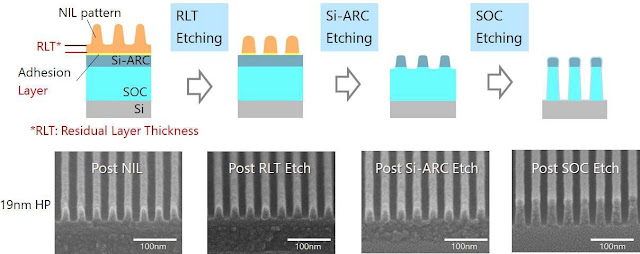
NIL utilizes a process where a patterned mask is brought into contact with a resist-coated substrate. The resist fills the relief patterns in the mask through capillary action, creating precise nano-scale features. With a focus on simplicity and cost-effectiveness, NIL doesn't require the complex optics found in traditional photolithography, making it an attractive option for semiconductor memory applications.
Early work on combining NIL and Atomic Layer Etching by AlixLabs Founders
Most Recent Achievements:
Recent study by TEL and Canon have demonstrated NIL's resolution capabilities of better than 10 nm, positioning the technology as a candidate for printing multiple generations of critical memory levels using a single mask. The potential to eliminate material waste by applying resist only where necessary adds to its appeal. Moreover, the simplicity and compactness of NIL equipment allow for clustered setups, enhancing productivity.
NIL Addressing Challenges in DRAM Scaling:
Dynamic Random Access Memory (DRAM) memory faces the challenge of continued scaling, with roadmap targets aiming at half pitches of 14 nm and beyond. The complexities of achieving tighter overlays, greater precision in critical dimensions, and edge placement errors demand innovative solutions. In DRAM fabrication, overlay requirements are even more stringent than in NAND Flash, with an error budget of 15-20% of the minimum half pitch.
Edge Placement Error (EPE):
EPE, the difference between intended and printed features, poses a significant challenge in modern semiconductor manufacturing. The intricacies of multiple patterning schemes and intricate device layouts contribute to EPE's complexity. Ensuring accurate placement of features is critical for maintaining device yield and performance.
The Quasi-Atomic Layer Etch (Quasi-ALE) process
The process is a specialized etching technique employed in advanced semiconductor manufacturing, particularly in processes like Nanoimprint Lithography (NIL). Quasi-ALE combines elements of Atomic Layer Etching (ALE) and conventional etching methods to achieve precise and controlled material removal. In the context of Nanoimprint Lithography, Quasi-ALE is used to etch materials with exceptional precision, targeting nanoscale features while minimizing damage to the surrounding areas. It involves a cyclic process where alternating etching and passivation steps are applied to the substrate. Each cycle removes a controlled layer of material, ensuring highly uniform etching and minimal lateral etch. One can discribe Quasi-ALE as a more productive way of performing ALE.
The key steps of the Quasi-ALE process typically involve:
1. Etch Step: During this step, a reactive gas is introduced into the etch chamber, which chemically reacts with the material to be removed. This reaction results in the selective removal of the material layer.
2. Passivation Step: In this step, a passivating species is introduced, forming a protective layer on the substrate surface. This layer prevents further etching and preserves the material beneath.
3. Purge and Repeat: The chamber is purged to remove any excess gases, and the process is repeated in a cyclical manner. Each cycle removes a controlled atomic layer of material.
Quasi-ALE is particularly advantageous for applications requiring high precision and control, such as in Nanoimprint Lithography, where maintaining accurate pattern dimensions and minimizing damage is critical. By combining the benefits of both ALE and traditional etching, Quasi-ALE enables advanced semiconductor manufacturing processes to achieve unprecedented levels of accuracy and uniformity.
Addressing EPE with Nanoimprint Lithography:
Researchers are actively exploring techniques to mitigate edge placement errors in nanoimprint lithography. This includes focusing on overlay accuracy, critical dimension uniformity (CDU), and local CDU. Compensatory methods such as dose control and reverse tone pattern transfer are being investigated to improve CDU and minimize errors.
The Role of Dose Control:
Varying the exposure dose offers a means of achieving small shifts in critical dimensions. Initial studies suggest that dose variations could lead to CD shifts of one to 2 nm. This strategy holds promise for enhancing CDU in the imprint process.
Reverse Tone Pattern Transfer:
Reverse tone processes, involving spin-on hard mask (SOHM) application and etch-back, offer an alternative approach to pattern transfer. While this method provides advantages such as reduced resist erosion and improved wall angles, trade-offs between CDU and line width roughness (LWR) need to be addressed.
Looking Ahead: The Possibilities and Challenges:
While NIL exhibits impressive potential, there are key challenges to overcome before it can be effectively integrated into high-volume semiconductor manufacturing. Ensuring precise overlay accuracy, managing complex CDU requirements, and effectively addressing edge placement errors remain pivotal. As the industry strives to achieve the roadmap's aggressive scaling targets, the evolution of nanoimprint lithography will undoubtedly play a crucial role.
Nanoimprint lithography is poised to reshape the semiconductor manufacturing landscape, offering higher resolution and cost-efficiency compared to traditional methods. With ongoing research and development, addressing challenges such as overlay accuracy, CDU, and EPE, the path to successful high-volume production through NIL seems promising. As technology continues to advance, the journey towards perfecting nanoimprint lithography is an exciting one, holding the potential to shape the future of chip fabrication.
Tokyo Electron (TEL):
TEL specializes in Nanoimprint Lithography (NIL) technology, offering precision equipment, advanced etching solutions, and expertise in process control. They excel in alignment, overlay correction, CDU management, and etching technology.
Canon:
Canon contributes to Nanoimprint Lithography (NIL) advancement by leveraging TEL's strengths in alignment, overlay correction, CDU management, and advanced etching solutions. They integrate these capabilities with the Reverse Tone Pattern Transfer, ensuring precise pattern replication and fidelity. Canon's focus on innovation drives high-resolution, cost-effective solutions for semiconductor manufacturing.
Canon has introduced a groundbreaking solution in the field of semiconductor technology with the development of the world's first mass-production equipment called the "FPA-1200NZ2C." This innovative tool utilizes nanoimprint lithography, a cutting-edge technique that involves imprinting nanometer-scale mask patterns onto substrates. By adopting this novel approach, Canon aims to overcome the limitations of conventional miniaturization methods. The FPA-1200NZ2C is already in use by Toshiba Memory, a prominent semiconductor memory manufacturer. This advancement marks a significant step forward in semiconductor manufacturing, enabling the creation of more intricate and advanced circuit patterns.
Sources:
High-Definition Nanoimprint Stamp Fabrication by Atomic Layer Etching — Lund University
Nanoimprint post processing techniques to address edge placement error (spiedigitallibrary.org)
Nanoimprint Lithography | Canon Global
FPD Lithography Equipment | Canon Global
Benefits of atomic-level processing by quasi-ALE and ALD technique - IOPscience
Acknowledgement :
Thanks for sharing the SPIE article on LinkedIn and giving insights Frederick Chen!
Monday, June 19, 2023
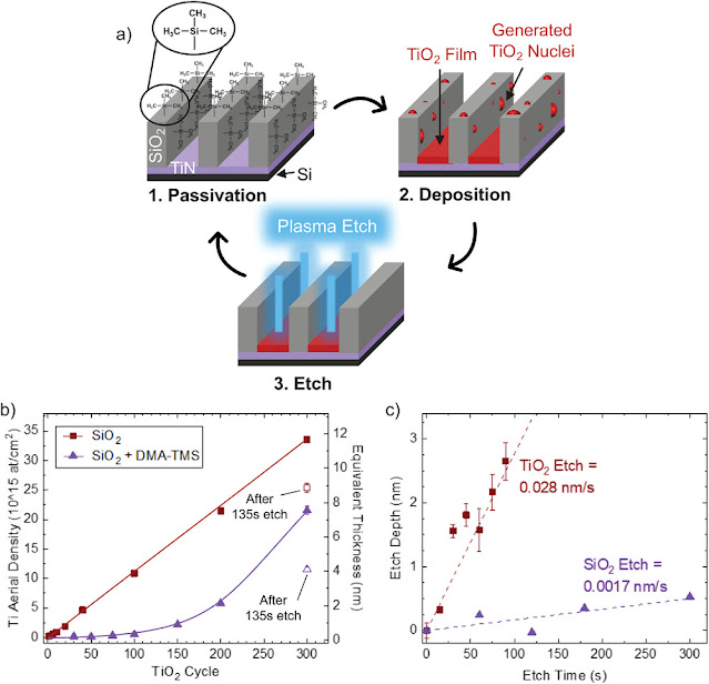
Revolutionary Study Unveils Enhanced Uniformity and Selectivity in TiO2 Films for Nanoelectronics Manufacturing
Researchers Achieve 2× Improvement in TiO2 Film Thickness and Pattern-dependent Uniformity in 45 nm Half-pitch Patterns
Wednesday, April 19, 2023
Call for Papers on ALD & ALE Applications, at ECS Fall Meeting / Gothenburg Oct. 2023 ►►DEADLINE EXPIRES APRIL 21◄◄
The Electrochemical Society (ECS) conference is an international event running every spring and fall, and gathering 2000-4000 participants and 30-40 exhibitors both from academia and industry.
The conference has a strong focus on emerging technology and applications in both electrochemistry and solid-state science & technology.
This fall the event will be held as 244th ECS Meeting on Oct. 8-12, 2023 in Gothenburg (Sweden).
The full program as well as information on travel assistance for students can be found on https://www.electrochem.org/
The organizers of symposium G01 on “Atomic Layer Deposition & Etching Applications, 19” encourage you to submit your abstracts on the following (and closely related) topics:
1. Semiconductor CMOS applications: development and integration of ALD high-k oxides and metal electrodes with conventional and high-mobility channel materials;
2. Volatile and non-volatile memory applications: extendibility, Flash, MIM, MIS, RF capacitors, etc.;
3. Interconnects and contacts: integration of ALD films with Cu and low-k materials;
4. Fundamentals of ALD processing: reaction mechanisms, in-situ measurement, modeling, theory;
5. New precursors and delivery systems;
6. Optical and photonic applications;
7. Coating of nanoporous materials by ALD;
8. MLD and hybrid ALD/MLD;
9. ALD for energy conversion applications such as fuel cells, photovoltaics, etc.;
10. ALD for energy storage applications;
11. Productivity enhancement, scale-up and commercialization of ALD equipment and processes for rigid and flexible substrates, including roll-to-roll deposition;
12. Area-selective ALD;
13. Atomic Layer Etching (‘reverse ALD’) and related topics aiming at self-limited etching, such as atomic layer cleaning, etc.
Abstract submission
Meeting abstracts should be submitted not later than the deadline of April 21, 2023 via the ECS website: Abstract submission instruction
List of invited speakers
· Johan Swerts, (Imec, Belgium) KEYNOTE: ALD challenges and opportunities in the light of future trends in electronics
· Stephan Wege (Plasway Technology, Germany), Reactor design for combined ALD & ALE
· Masanobu Honda (TEL, Japan), Novel surface reactions in low-temperature plasma etching
· Barbara Hughes, (Forge Nano, USA), Dual Coatings, Triple the Benefit; Atomic Armor for Better Battery Performance
· Juhani Taskinen, (Applied Materials-Picosun, Finland), ALD for biomedicine
· Alex Kozen (Univ. of Maryland, USA), ALD for improved Lithium Ion Batteries
· Malachi Noked (Bar-Ilan Univ., Israel), ALD/MLD for batteries
· Yong Qin (Chinese Academy of Sciences), ALD for catalysis
· Jan Macák, (Univ. of Pardubice, Czechia), ALD on nanotubular materials and applications
· Bora Karasulu, Univ. of Warwick, UK), Atomistic Insights into Continuous and Area-Selective ALD Processes: First-principles Simulations of the Underpinning Surface Chemistry
· Ageeth Bol (Univ. Michigan, USA), ALD on 2D materials
· Pieter-Jan Wyndaele (KU Leuven-imec, Belgium), Enabling high-quality dielectric passivation on Monolayer WS2 using a sacrificial Graphene Oxide template
· Elton Graugnard (Boise State Univ., USA), Atomic Layer Processing of MoS2
· Han-Bo-Ram Lee (Incheon National Univ., Korea), Area-Selective Deposition using Homometallic Precursor Inhibitors
· Ralf Tonner (Univ. Leipzig, Germany), Ab initio approaches to area-selective deposition
· Nick Chittock (TU Eindhoven, Netherlands), Utilizing plasmas for isotropic Atomic Layer Etching
· Heeyeop Chae (Sungkyunkwan Univ., Korea), Plasma-enhanced Atomic Layer Etching for Metals and Dielectric Materials
· Charles Winter (Wayne State Univ., USA), New Precursors and Processes for the Thermal ALD of Metal Thin Films
· Anjana Devi, Ruhr Univ. Bochum, Germany), Novel precursors dedicated for Atomic Layer Processing
Visa and travel
For more information, see: www.electrochem.org/244/visa-
In addition, Mrs. Francesca Spagnuolo at the ECS (Francesca.Spagnuolo@
We are looking forward to meeting you in Gothenburg !
Tuesday, November 8, 2022
Recent ALD news on shared on Twitter #ALDep
Area Selective ALD of Ruthenium #ALDep #ASDep https://t.co/LInkrCfXNf
— Jonas Sundqvist 🐳 (@jv3sund) November 7, 2022
TOPCon solar cell achieves 24.2% efficiency via new plasma-assisted atomic layer deposition tech from Nantong University, China#ALDep #solar #solarcell #china #photovoltaic https://t.co/VjMBvz8Ib0
— Jonas Sundqvist 🐳 (@jv3sund) November 7, 2022
Researchers at the @HelsinkiALD are developing thin films needed in new types of halide perovskite solar cells, and matching #ALDep processeshttps://t.co/JzBSalKiuN pic.twitter.com/tWv4WMAgvA
— Jonas Sundqvist 🐳 (@jv3sund) November 4, 2022
University of Erlangen demonstrate sALD of Crystalline Metal–Organic Framework Thin Films (MOFs)#ALDep #MOFs https://t.co/cUgGOWkJjl pic.twitter.com/B1l0S4qQM7
— Jonas Sundqvist 🐳 (@jv3sund) November 4, 2022
Abstract submission is now open for the AVS 23rd International Conference on Atomic Layer Deposition (#ALD2023) and the 10th International Atomic Layer Etching Workshop (#ALE2023). Deadline: Feb. 15, 2023. https://t.co/QvY8bu8KPp #ALDep #ALEtch @AVSALD https://t.co/x2MrKttxk9 pic.twitter.com/BgYxx19FHK
— AVS (@AVS_Members) November 2, 2022
Monday, September 26, 2022
AlixLabs proudly announce its Advisory Board
Sunday, September 4, 2022
3D Printing by ALD with Atlant 3D's Maksym Plakhotnyuk - ALD Stories
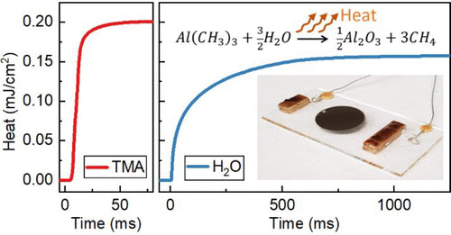
Resolving the Heat of Trimethylaluminum and Water Atomic Layer Deposition Half-Reactions
J. Am. Chem. Soc. 2022, 144, 33, 15203–15210
Publication Date:August 9, 2022
https://doi.org/10.1021/jacs.2c05460
Wednesday, August 31, 2022
Webinar Atonarp’s Aston in-situ metrology solution for Spatial ALD
|
|
|


%20(1).png)


