Showing posts with label BEOL. Show all posts

Friday, June 15, 2018

Cobalt and Ruthnium confirmed in Intel 10nm Cannon Lake BEOL

TechInsights has found the long-awaited Cannon Lake - the Intel 10 nm logic process inside the i3-8121U CPU, used in the Lenovo IdeaPad330.
 
This innovation boasts the following:

  • Logic transistor density of 100.8 mega transistors per mm2, increasing 10nm density 2.7X over the 14nm node
  • Utilizes third generation FinFET technology
  • Minimum gate pitch of Intel’s 10 nm process shrinks from 70 nm to 54 nm
  • Minimum metal pitch shrinks from 52 nm to 36 nm
Process Highlights:

  • Deepest scaled pitches of current 10 nm and upcoming 7 nm technologies
  • First Co metallization and Ru usage in BEOL
  • New self-aligned patterning schemes at contact and BEOL
Source: TechInsight (LINK)

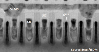
By reading this it is not possible to determine exactly how Ruthenium is used or how it has been deposited and there are several options like barrier and seed layer for plating Copper or Cobalt. What is known is that Intel presented already at IEDM2017 the use of cobalt in their 10 nm MOL/BEOL process flow as contacts and M0/M1 lines as well as barrier/seed for copper and copper cap for complete encapsulation of copper up to M5.


Intel 10nm mid end of line cobalt and copper metallization as presented at IEDM 2017.

Wednesday, June 6, 2018

Applied Materials enables cobalt contact & interconnect for 7nm with pre-clean, PVD, ALD and CVD – on the Endura® platform

At IEDM 2017 in December both Intel and Globalfoundries presented cobalt encapsulation (liner and cap) for copper local interconnects as well as Co fill contacts for their 10nm resp 7nm technologies. Since then many have wondered about the unit process details behind the new cobalt integration and here we have it - The Applied Materials  complete cobalt solution as announced yesterday. Especially interesting that TiN ALD also is used as a cobalt seed/adhesio/dufusion barrier for cobalt contacts. The most interesting stuff you will finde here: LINK
[SANTA CLARA, Calif., June 05, 2018]  Applied Materials, Inc. today announced a breakthrough in materials engineering that accelerates chip performance in the big data and AI era.

In the past, classic Moore’s Law scaling of a small number of easy-to-integrate materials simultaneously improved chip performance, power and area/cost (PPAC). Today, materials such as tungsten and copper are no longer scalable beyond the 10nm foundry node because their electrical performance has reached physical limits for transistor contacts and local interconnects. This has created a major bottleneck in achieving the full performance potential of FinFET transistors. Cobalt removes this bottleneck but also requires a change in process system strategy. As the industry scales structures to extreme dimensions, the materials behave differently and must be systematically engineered at the atomic scale, often under vacuum. 
To enable the use of cobalt as a new conducting material in the transistor contact and interconnect, Applied has combined several materials engineering steps – pre-clean, PVD, ALD and CVD – on the Endura® platform. Moreover, Applied has defined an integrated cobalt suite that includes anneal on the Producer® platform, planarization on the Reflexion® LK Prime CMP platform and e-beam inspection on the PROVision™ platform. Customers can use this proven, Integrated Materials Solution to speed time-to-market and increase chip performance at the 7nm foundry node and beyond. 

“Five years ago, Applied anticipated an inflection in the transistor contact and interconnect, and we began developing an alternative materials solution that could take us beyond the 10nm node,” said Dr. Prabu Raja, senior vice president of Applied’s Semiconductor Products Group. “Applied brought together its experts in chemistry, physics, engineering and data science to explore the broad portfolio of Applied’s technologies and create a breakthrough Integrated Materials Solution for the industry. As we enter the big data and AI era, there will be more of these inflections, and we are excited to be having earlier and deeper collaborations with our customers to accelerate their roadmaps and enable devices we never dreamed possible.”

While challenging to integrate, cobalt brings significant benefits to chips and chip making: lower resistance and variability at small dimensions; improved gapfill at very fine dimensions; and improved reliability. Applied’s integrated cobalt suite is now shipping to foundry/logic customers worldwide.

Applied Materials, Inc. (Nasdaq:AMAT) is the leader in materials engineering solutions used to produce virtually every new chip and advanced display in the world. Our expertise in modifying materials at atomic levels and on an industrial scale enables customers to transform possibilities into reality. At Applied Materials, our innovations make possible the technology shaping the future. Learn more at www.appliedmaterials.com.

Monday, January 1, 2018

Aveni extends copper interconnects to 5nm and below for BEOL integration employing ALD TaN & CVD Co barrier/seed

Recently at IEDM 2017 IBM announced that copper is here to stay and can continue to be scaled for the future back end of line (BEOL) interconnects - 20 Years of Cu BEOL in Manufacturing, and its Future Prospects (Invited), D. Edelstein, IBM TJ Watson Research Center (LINK)

Before the actual copper plating process, the advanced dual-damascene structures for interconnects employ two very important conformal deposition processes :
  • an atomic layer deposition tantalum nitride (ALD TaN) copper diffusion barrier
  • a thin chemical vapor deposition cobalt (CVD Co) liner
More detailed information on Cobalt CVD for barrier/seed and selective encapsulation of copper from the leader Applied Materials can be found here (LINK).

According to a press release below (LINK), Aveni has announced it has obtained results that support the continued use of copper in the BEOL for advanced interconnects, at and beyond the 5nm technology node. Aveni is a French developer and manufacturer of wet deposition technologies and chemistries for 2D interconnects and 3D through silicon via packaging. The company was originally founded in 2001 as a spinoff from the Commissariat à l’énergie atomique et aux énergies alternatives (CEA) to develop and market groundbreaking nanometric deposition technologies for a variety of electronic applications.  

MASSY, France – Dec. 12, 2017 – aveni S.A., developer and manufacturer of market-disrupting wet deposition technologies and chemistries for 2D interconnects and 3D through silicon via packaging, today announced it has obtained results that strongly support the continued use of copper in the back end of line (BEOL) for advanced interconnects, at and beyond the 5nm technology node.

Saturday, July 30, 2016

Wayne State presented new ALD chemistries for low temperature tantalum and selective cobalt at ALD2016

Prof. Chuck Winter and his team at Wayne State presented new ALD chemistries for low temperature tantalum and selective cobalt at ALD 2016 Ireland this week. Both processes are very important for todays scaling of logic and memory technologies. Metallic tantalum can be used in workfunction engineering of HKMG high performance FinFET transitors as well as for Cu seed/barrier technology in BEOL. Cobalt is as tantantlum an option for Cu barrier/seed and also used selectivly to cap the Cu lines and vias from oxidising and reducing RC performance.


The best highlight talk went to Marissa Kerrigan from Wayne State as voted by attendees on novel Co recursor chemistry for selective Cobalt (Left Marissa Kerrigan, right Simon Elliott, photo by ALD2016.com).

“This opens up the prospect of using tantalum in layers just a few nanometers thick as the liner for interconnect wiring in the complex geometries of next-generation electronic chips,” said the University, which worked with German chemicals giant BASF on the project accoring to Electronic Weekly.

Marissa Kerrigan also from Wayne State announced novel ALD chemistry for metallic cobalt that showed excellent selectivity to copper (photo by ALD2016.com).

“The Wayne State processes for tantalum and cobalt are significant steps forward in controlled growth of ultra-thin metals,” said conference chair, Dr Simon Elliott of Ireland’s Tyndall National Institute. “Strong growth is projected for area-selective deposition: in the near future, it will allow higher-precision patterning of semiconductor chips, and in the longer term it will be an enabler for manufacturing nano-structured materials on demand.” according to the same article in Electronics Weekly.

Tuesday, January 5, 2016

ALD & CVD Metal Manganese Precursors from Canada


The other day we had a paper by Barry Lab on how to make your own gold ALD precursor and now here another hot topic in ALD & CVD of Metal Manganese and for sure also this paper is from Canada as well! Manganese is being evaluated by Intel, Imec and others for sub 10 nm Cu barrier in BEOL metallization. Even if those barriers are just a couple of nano meters thin it is big business since the potential in BEOL is huge if the processes were to be used for a multiple wafer passes of the BEOL Cu metallization. Recently at 20/14 nm. It will be interesting to follow if Manganese will put up a fight against Cobalt or the slugger Ruthenium for future interconnect barriers and Cu caps.

Base-Free and Bisphosphine Ligand Dialkylmanganese(II) Complexes as Precursors for Manganese Metal Deposition

Jeffrey S. Price, Preeti Chadha, and David J. H. Emslie
Organometallics, Article ASAP, DOI: 10.1021/acs.organomet.5b00907
Publication Date (Web): December 30, 2015


Graphical abstract
 

The solid-state structures and the physical, solution magnetic, solid-state magnetic, and spectroscopic (NMR and UV/vis) properties of a range of oxygen- and nitrogen-free dialkylmanganese(II) complexes are reported, and the solution reactivity of these complexes toward H2 and ZnEt2 is described. The compounds investigated are [{Mn(μ-CH2SiMe3)2}] (1), [{Mn(CH2CMe3)(μ-CH2CMe3)2}2{Mn(μ-CH2CMe3)2Mn}] (2), [Mn(CH2SiMe3)2(dmpe)] (3; dmpe = 1,2-bis(dimethylphosphino)ethane), [{Mn(CH2CMe3)2(μ-dmpe)}2] (4), [{Mn(CH2SiMe3)(μ-CH2SiMe3)}2(μ-dmpe)] (5), [{Mn(CH2CMe3)(μ-CH2CMe3)}2(μ-dmpe)] (6), [{Mn(CH2SiMe3)(μ-CH2SiMe3)}2(μ-dmpm)] (7; dmpm = bis(dimethylphosphino)methane), and [{Mn(CH2CMe3)(μ-CH2CMe3)}2(μ-dmpm)] (8). Syntheses for 14 have previously been reported, but the solid-state structures and most properties of 24 had not been described. Compounds 5 and 6, with a 1:2 dmpe/Mn ratio, were prepared by reaction of 3 and 4 with base-free 1 and 2, respectively. Compounds 7 and 8 were accessed by reaction of 1 and 2 with 0.5 equiv or more of dmpm per manganese atom. An X-ray structure of 2 revealed a tetrametallic structure with two terminal and six bridging alkyl groups. In the solid state, bisphosphine-coordinated 38 adopted three distinct structural types: (a) monometallic [LMnR2], (b) dimetallic [R2Mn(μ-L)2MnR2], and (c) dimetallic [{RMn(μ-R)}2(μ-L)] (L = dmpe, dmpm). Compound 3 exhibited particularly desirable properties for an ALD or CVD precursor, melting at 62–63 °C, subliming at 60 °C (5 mTorr), and showing negligible decomposition after 24 h at 120 °C. Comparison of variable-temperature solution and solid-state magnetic data provided insight into the solution structures of 28. Solution reactions of 1-8 with H2 yielded manganese metal, demonstrating the thermodynamic feasibility of the key reaction steps required for manganese(II) dialkyl complexes to serve, in combination with H2, as precursors for metal ALD or pulsed CVD. In contrast, the solution reactions of 18 with ZnEt2 yielded a zinc–manganese alloy with an approximate 1:1 Zn/Mn ratio.

Saturday, December 12, 2015

MAM2016 & HERALD ALD for BEOL Workshop in Brussels March 20th

MAM 2016 will be the 25th in a series devoted to research on materials properties and interactions of interconnect and silicide materials.  Starting as a workshop on refractory metals and silicides in the 1980’s and moving towards materials for advanced metallization in 1995, the 2016 conference also aims to address new challenges in the fields of Materials for Flexible Electronics,


Thursday, December 10, 2015

The limits of ALD barrier seed for Cu metallization

Here is a great piece by ED KORCZYNSKI, Senior Technical Editor at Solid State Technology on the practical limits for metallization beyond 14nm tthat inspired me too dig into ALD Mn self forming barriers.


Ed states that one of the limitation for Cu metallization will actually be how thin you can deposit an ALD barrier/seed layer (see figure below).


Wednesday, July 15, 2015

Imec introduces self-assembled monomolecular organic films to seal ultra-porous low- k materials

Nano-electronics research center imec announced today at SEMICON West that it has demonstrated concept and feasibility for pore-sealing low-k dielectrics in advanced interconnects. The method, based on the self-assembly of an organic monolayer, paves the way to scaling interconnects beyond N5. 


RC plot and HAADF-STEM images illustrating the effectiveness of SAM sealing in preventing metal indiffusion into the ultra-porous low-k film integrated in a 45nm half pitch dual damascene test vehicle. This translates in a 30% decrease in the measured capacitance. (www.imec.be)
The need for ultra-porous low-k materials as interconnect dielectrics to meet the requirements dictated by the ITRS (International Technology Roadmap for Semiconductors) poses several challenges for successful IC integration. One of the most critical issues is the indiffusion of moisture, ALD/CVD metal barrier precursors and Cu atoms into the porous low-k materials during processing (low-k pore diameter larger than 3nm, up to 40% porosity). This leads to a dramatic increase of the material dielectric constant and leakage current, and to the reduction of the voltage for dielectric breakdown.


Imec has developed a method to seal the pores of the low-k material with a monomolecular organic film. The method not only prevents diffusion of moisture and metal precursors into the low-k material, it also might provide an effective barrier to confine copper within the copper wires and prevent copper diffusion into the low-k material.

Self-assembled monolayers (SAMs) derived from silane precursors, are deposited from vapor phase on 300mm wafers into low-k during chemical vapor or atomic layer deposition and subsequent Cu metallization. The dielectric constant (k) of the resulting sealing layer is 3.5 and a thickness lower than 1.5nm was achieved. This is key to limit the RC delay increase enabling beyond 5nm technology nodes. As a result, a ca. 30% capacitance reduction was observed after SAM pore-sealing was applied. Moreover, a clear positive impact on the low-k breakdown voltage is observed upon sealing.