Showing posts with label ALE - Atomic Layer Etching. Show all posts

Saturday, June 12, 2021

Vinova fund Swedish AlixLabs Breakthrough green technology in Nanostructures Miniaturization for Electronic Chips

Vinnova has decided to grant AlixLabs application to Innovative Startups step 2 "Breakthrough green technology in Nanostructures Miniaturization for Electronic Chips" in the spring of 2021. 140 applications were received for the call, of which 35 were given grants. The assessment is based on a weighting of the six main criteria Relevance, Potential, Team, Implementation, Sustainability, and Gender Equality. The applications have been assessed in competition with each other. AlixLabs application was judged to meet the criteria to a great extent. 

AlixLabs aim to validate our breakthrough green technology for nanofabrication of nanostructures for applications in electronic chips. It is to demonstrate that Alixlabs' method is technically viable for the production of low dimensional transistors down to 2 nm node size, in line with the newly designed European Flagship "A European Initiative on Processors and semiconductor technologies" (LINK) to develop next-generation chips and 2 nm technology with €146.5 B, supported by 22 EU members. This demonstration will minimize the risks for AlixLabs entering the semiconductor industry market and ecosystem.


Miniaturization of electronic components, known as Moore's law, is fundamental to the entire IT explosion leading to the fast processing of data. Production of sub 10 nm chips requires advanced equipment such as extreme UV lithography (EUVL) tools, costing over €100 million, not affordable to all manufacturing companies or adding extreme investment cost for those companies still in the scaling race. Our innovative patented technology (WO2017157902A1) enables miniaturization without requiring or reducing the number of process steps using costly EUVL. This way, less financially powerful manufacturers (fabs) can get back to semiconductor production chains on level terms with large competitors from the USA and Asia. Our technology uses Atomic Layer Etching (ALE) for pitch splitting of nanostructures, which allows for efficient and high-volume nanopatterning and offers to reduce operating cost up to 35 - 50% and energy use and greenhouse emissions by 25 - 50% per Lithography mask layer requiring advanced Immersion base multiple patterning technology or EUVL single and double exposure.

BREAKTHROUGH DEVELOPMENTS

We envision two breakthrough developments in this project:

(1) Application of ALE pitch splitting nanofabrication for electronic chip manufacturing down to 2 nm Foundry node size
(2) Demonstration of first transistors produced by ALE pitch splitting

Vinnova is the Swedish government agency that administers state funding for research and development. The agency's mission as defined by the government is to promote the development of efficient and innovative Swedish systems within the areas of technology, transportation, communication and labour.

About AlixLabs AB:

AlixLabs (www.alixlabs.com) is an innovative startup enabling the semiconductor industry to scale down Logic and Memory components in a cost-effective manner by the use of ALE Pitch Splitting (APS).

Background Information:


Thursday, May 20, 2021

ALD/ALE 2021 Technical Program June 27-30, 2021

Virtual Meeting Overview & Highlights

The AVS 21st International Conference on Atomic Layer Deposition (ALD 2021) featuring the 8th International Atomic Layer Etching Workshop (ALE 2021) will be adapted into a Virtual Meeting comprised of Live and On Demand Sessions. The event will feature:

AVS ALD/ALE 2021 Conference Page 

Live Tutorial Session with live Q&A Chat Opportunities
(Sunday, June 27, 2021)

  • Parag Banerjee (University of Central Florida, USA), “Seeing Is Believing: In situ Techniques for Atomic Layer Deposition (ALD) Process Development and Diagnostics”
  • Arrelaine Dameron (Forge Nano, USA), “ALD Powder Manufacturing”
  • Henrik Pedersen (Linkoping University, Sweden), “Let’s Talk Dirty – Battling Impurities in ALD Films”
  • Riikka Puurunen (Aalto University, Finland), “Fundamentals of Atomic Layer Deposition: An Introduction (“ALD 101”)”
  • Fred Roozeboom (Eindhoven University of Technology, The Netherlands), “ALE and ALD: Two Biotopes of a Kind in Atomic-Scale Processing”

Live Plenary, Awards, and Student Finalists with live Q&A Chat Opportunities (Monday, June 28, 2021)

  • Plenary Speaker: Steven George (University of Colorado Boulder, USA), “Mechanisms of Thermal Atomic Layer Etching”
  • Plenary Speaker: Todd Younkin (Semiconductor Research Corporation, USA), “Materials & Innovation – Essential Elements that Underpin the Next Industrial Revolution
  • Live Parallel Technical Sessions with live Q&A Chat Opportunities (Tuesday-Wednesday, June 29-30, 2021)

  • On Demand Oral Sessions (Starting Monday, June 28, 2021)

  • On Demand Poster Sessions with a Mix of Pre-recorded (Video or Audio) Talks and/or PDF files

Note: Live and On Demand Sessions available on Mobile App/Online Scheduler through July 31, 2021 and then to AVS members in the AVS Technical Library. Live Sessions will also be recorded and added to the On Demand Sessions.

Thursday, May 13, 2021

Schweden wollen mit Ätz-Spalttechnik Chipproduktion in Sachsen umkrempeln

Alix Labs aus Lund testet Verfahren nun im Silicon Saxony, berichtet Heiko Weckbrodt bei Oiger.de


Lund/Bannewitz, 13. Mai 2021. Ingenieure aus Schweden und Sachsen wollen gemeinsam die Mikroelektronik-Produktion umkrempeln. Dafür hat das schwedische Technologie-Unternehmen „Alix Labs“ ein Verfahren entwickelt, das die Produktion neuester Computerchips mit Strukturgrößen unterhalb von zehn Nanometern (Millionstel Millimeter) stark vereinfachen und verbilligen soll. Dabei geht es auch darum, den Einsatz teurer Belichtungsanlagen mit „Extremer Ultraviolett-Strahlung“ (EUV) zu vermeiden, die etwa 120 Millionen Euro pro Maschine kosten und für die es weltweit nur eine Quelle gibt: ASML aus den Niederlanden. Um auf alternativen Wegen feinste Chipstrukturen zu erzeugen, setzen die Schweden auf eine „Pitch-Splitting-Methode“ (APS) mittels Atomlagen-Ätzen (Atomic Layer Etching, abgekürzt ALE). „Plasway Technologies“ aus Bannewitz in Dresden transferiert dieses Verfahren nun in einen industrienahen Maßstab auf 300 Millimeter großen Siliziumscheiben (Wafer).
Weiterlesen: LINK


„In Schweden haben wir keine 300-Millimeter-Infrastruktur“, erklärt „Alix Labs“-Chef Jonas Sundqvist die Kooperation mit den Sachsen. „Unsere Technologie kann in bestehende Prozessabläufe der Halbleiterherstellung integriert werden. Theoretisch könnten Chipfabriken wie die Globalfoundries-Fab 1 in Dresden unsere Methode einführen und dann 10- oder 7-Nanometer-Chips herstellen ohne teure EUV-Anlagen.“ Als Kunden sieht er aber auch Branchenriesen wie Intel, TSMC und Samsung.

Friday, April 30, 2021

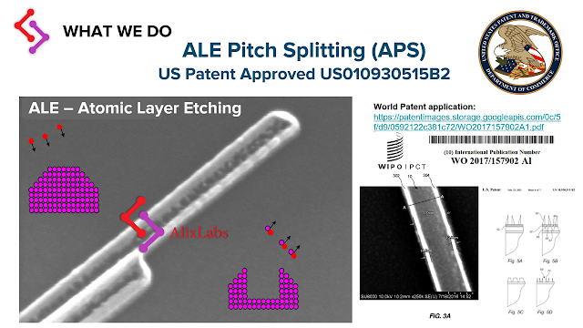
The US Patent Office has approved AlixLabs’ patent application for nanofabrication by ALE Pitch Splitting (APS)

(30 April 2021, Lund Sweden). The US Patent Office has approved AlixLabs’ (AlixLabs AB) patent application for nanofabrication by ALE Pitch Splitting (APS).

The US Patent Office has issued a patent (US10930515) on February 23, 2021. The patent covers methods to split nanostructures in half by a single process step using Atomic Layer Etching (ALE). The method has the potential to have a big impact on the semiconductor industry by enabling sustainable scaling of electronic components and shrink chip designs further in a cost-effective way. The method is complementary for single exposure Immersion and Extreme UV (EUV) Lithography and corresponding multiple patterning technologies like self-aligned double and quadruple patterning (SADP resp. SAQP) as well as directed self-assembly (DSA).

In direct comparison to mentioned more complicated and expensive methods, APS may cut the need for certain fab equipment investments considerably, reduce manufacturing cost and energy consumption as well as reduce greenhouse gas emission during the patterning processing by up to 50%, allowing greener and affordable way forward for the semiconductor industry.

AlixLabs aims at applications for the manufacturing of leading-edge sub 5nm Logic Devices and Memory Chips that are used for everyday consumer electronic devices, 5G and AI.

The company’s CEO Dr. Jonas Sundqvist comments:

After founding the company in 2019 we now move into very exciting times. The team has been expanded with Dr. Mohammad Karimi as Principal Scientist and we have several applications and projects in the pipeline for broadening our patent protection and creating further opportunities for commercial agreements starting now. Currently, we are taking on the first round of private investments and will expand operations for both core activities in Lund, Sweden, at NanoLund and Lund Nano Lab, and the IDEON Science Park in Sweden. In addition, we are heading to the heart of the European semiconductor industry in Dresden Germany for a lab to fab transfer to 300 mm silicon wafer process verification to get ready for customer demonstrations of APS.

The company’s CTO Dr. Dmitry Suyatin comments:

This patent is built on a surprising discovery by the inventors, which took place at Lund Nano Lab during the Master project by Dr. Sabbir A. Khan who has recently received his PhD from the University of Copenhagen and now continues his postdoctoral work at Niels Bohr Institute in Copenhagen.

About AlixLabs AB:

AlixLabs (www.alixlabs.com) is an innovative startup enabling the semiconductor industry to scale down Logic and Memory components in a cost-effective manner by the use of ALE Pitch Splitting (APS).

Background Information:


Picture:


Monday, April 5, 2021

ALD/ALE 2021 is Going Virtual June 27-30, 2021

ALD/ALE 2021 is Going Virtual June 27-30, 2021 due to the Covid19 situation.

Virtual Meeting Overview & Highlights

The AVS 21st International Conference on Atomic Layer Deposition (ALD 2021) featuring the 8th International Atomic Layer Etching Workshop (ALE 2021) will be adapted into a Virtual Meeting comprised of Live and On Demand Sessions. The registration deadline is June 30, 2021; all presenters must register by May 1, 2021. The event will feature:
  • Live Tutorial Session with live Q&A Chat opportunities (Sunday, June 27, 2021)
  • Live Plenary, Awards, and Student Finalists with live Q&A Chat opportunities (Monday, June 28, 2021)
  • Live Parallel Technical Sessions with live Q&A Chat opportunities (Tuesday-Wednesday, June 29-30, 2021)
  • On Demand Oral Sessions (Starting Monday, June 28, 2021)
  • On Demand Poster Sessions with a Mix of Pre-recorded (Video or Audio) Talks and/or PDF files
  • Live and On Demand Sessions available on Mobile App/Online Scheduler through July 31, 2021 and then to AVS members in the AVS Technical Library

AVS ALD/ALE 2021 Web

Note: Live Sessions will also be recorded and added to the On Demand Sessions.


ALD Program Chairs
 
Program Chair:
Seán Barry (Carleton University, Canada)

Program Co-Chair:
Scott Clendenning (Intel, USA)
ALE Program Chairs

Program Chair:
Jane Chang (University of California, Los Angeles, USA)

Program Co-Chair:
Thorsten Lill (Lam Research, USA)

Thursday, March 18, 2021

AlixLabs AB launched ALE Pitch Splitting (APS) for the first time at ALD & ALE Ireland 2016

We did not want to steal the thunder from our good Irish friends and St. Patrick Day we wish you all a healthy recovery today and breakfast for Champions. Yesterday we remembered our trip to Dublin and launching our proprietary technology, APS - ALE Pitch Splitting, for the first time to a bigger audience. Since then a lot of things has happened at AlixLabs AB in Lund, Sweden:

  • We received soft funding and invest support to found the company by LU Holding (LINK) - AlixLabs AB in Lund, Sweden operating out of IDEON Science park (LINK) and Lund Nano lab at Lund University
  • We received SwedishVinnova grant for "Innovative startups" 93 startup-bolag får dela på 28 miljoner | Vinnova
  • We hired our first Full-time employee Dr. Mohammad Karim, Principal Scientist (LINK)
  • We signed an agreement to use the lab facilities of Sweden’s largest research environment for nanoscience and nanotechnology - Lund Nano Lab (LINK)
  • We applied for an Additional 2.7 MSEK EU and National Swedish Soft co-funding in early 2021 and have additional 3 projects in the pipeline.
  • We have started our 1st Investment round to close before Swedish Midsummer - please get in touch if you want a meeting! (jonas@alixlabs.com or LinkedIn: LINK)


ALE Pitch Splitting (APS) taking place at the Lund Nano Lab exhibition stand in the ALD Ireland 2016 Industry Exhibition.

Video from presentation invited given by Dr. Dmitry Suyatin LINK. Staff Engineer at Lund Nano Lab and CTO of AlixLabs AB and on the Scientific Committee of AVS ALE.


A possible starting point of ALE Pitch Splitting explained best using Guinness Beer Barrels.


Prof. Samuelson from Lund University opening ALD Ireland 2016


Dr. Simon Elliott, main Chair of the Conference, teaching us how to tap a Guinness with a perfect solid head. Then at Tyndall National Institute and now Director of  Atomic Level Simulation at Schrödinger.


Dr. Dmitry Suyatin AlixLabs to be CTO at the Poster Session after his invited talk on ALE Pitch Splitting (Abstract LINK).


Interesting discussions with the Inventor of the Entegris/ATMI ProEvap Technology, Ravi Laxman, for solid precursor delivery in HVM at all the leading IDMs and Foundries since 2007.


Social Event by Air Liquide and Picosun at The Temple Bar in Dublin


Social Event by Air Liquide and Picosun at The Temple Bar - all enjoying a few pints of Guinness.


Industry panel on the future of ALD and ALE with the leading expertise Prof. Ritala (Helsinki University, Prof Roozeboom (TU Eindhoven/TNO), Dr. Suvi Haukka (ASM Micro Chemistry), Dr. Jean Marc Girard (Air Liquide and Dr. David Thompson (Applied Materials)


Moderation by ALD2016 Co-ChairDr. Jonas Sundqvist, then Operation Manager of Lund Nano Lab.


Green Beam splitting at the Gala Dinner & Award ceremony.


The fantastic Conference Centre in Dublin by night, The Convention CentreDocklands, Dublin 

All photos above by Herr und Frau Dr. Knaut (C)2016 (https://www.katharinaknaut.com/index.php?seite=archiv&name=201608jonasald)


Tuesday, March 9, 2021

April 6-8 5th Area Selective Deposition Workshop (ASD 2021)

In an effort to help facilitate the progression of ASD techniques, The University of Texas at Austin University is proud to host the 5th Area Selective Deposition Workshop (ASD 2021), which will be held on April 6-8, 2021. The Area Selective Deposition Workshop scheduled for April 2-3 (ASD 2020) was postponed in March 2020 due to public health concerns relating to the coronavirus disease (COVID-19) and was later canceled in anticipation of ASD 2021. ASD 2021 retains much of the character of previous workshops and what was intended for ASD 2020, albeit in a virtual format. This year’s workshop will act as a central event for sharing and discussing the newest developments in ASD by gathering leading experts from both academia and industry. Attendees can expect to participate in talks regarding fundamental challenges related to recent developments in ASD, applications for ASD in next-generation technology, emergent processes for implementing ASD techniques, and new perspectives on metrological and characterization strategies for further understanding persistent mechanistic challenges.
Key Deadlines:
Early Registration Deadline: March 16, 2021
Questions? Contact ekerdt@utexas.edu


The workshop will begin at 10:00 am (CST) and end at 3:00 pm on April 6 and 7 and at 2:00 pm on April 8. Times have been selected to enable participation for registrants spanning the West Coast to Europe. The workshop will include live sessions consisting of invited and contributed talks and panel discussions. A session moderator will ask questions that are entered onto the meeting presentation platform from registrants. Live poster sessions will be held after the oral presentation sessions on April 6 and 7; poster presenters will preload five-minute oral highlights of their poster one week before the workshop.

Invited speakers:
    • Chris Bates, UC Santa Barbara, USA
    • Fabio Grillo, ETH Zurich, Switzerland
    • Ravi Kanjolia, EMD Electronics, USA
    • Shashank Misra, Sandia National Labs, USA
    • Ainhoa Romo Negreira, TEL, Belgium
    • Tania Sandoval, Universidad Técnica, Chile
    • Kavita Shah, Nova, USA
    • Amy Walker, UT Dallas, USA
    • Charles Wallace, Intel, USA

Saturday, March 6, 2021

Thermal ALE of germanium rich SiGe by CU Boulder and ASM Microchemistry

Epitaxially grown SiGe is an important material for CMOS Logic. It is integrated as the channel material and by inserting a higher concentration of germanium the mobility of the transistor can be improved. The industry calls it Epi, but what is really referred to a thermal CVD process producing an epitaxially grown layer of silicon or silicon-germanium onto a single crystalline silicon wafer.

As CMOS scaling has progressed the IDMs and Foundries have moved from the planar field-effect transistor (FET) architecture to a narrow fin-based transition the FinFET. The next evolutionary step on the horizon will be the transition to a nanowire-based architecture forming a gate-all-around FET (GAA-FET). At some point in time beyond the 2 nm node, the lateral scaling possibility will hit a wall and it is foreseen that the CMOS scaling will gup upwards like other technologies in order to cram in more devices per unit area. In a first approach, it may be that the NMOS and PMOS transistors are rearranged from being processed next to each other to put one of them on top of the other. Intel recently presented this at IEDM2020 (LINK). Having done that you can foresee continuing on a vertical scaling path also for CMOS just like 3DNAND and start to build those skyscrapers.

When going vertical, you will need highly conformal deposition processes as provided by ALD and in high volume production since the event of 90 nm DRAM (Samsung) and 45 nm Logic (Intel), however, etch is a problem since the reactive ion etching process are typically directional with the plasma under low-pressure processing conditions used. Also, the Argon plasma ALE processes to etch Silicon, silicon Germanin gallium nitride, and III/V materials are directional or anisotropic as the etch guys say or non-conformal as we ALD people say.

Typically the best way to achieve isotropic etch conditions, meaning you remove material at the same rate or as for ALE the same amount per cycle (etch per cycle EPC), is to skip the plasma that causes the anisotropic etch. Here Dr Abdulgatov and co-workers in the famous SM George Lab, CU Boulder together with Varun Sharma and friends from ASM Microchemistry, one of Dresden's best shining ALD-Stars, publish a paper on Thermal ALE of germanium rich SiGe that is quite clever. Here using PVD Si0.15Ge0.85 samples, which are difficult to make by Epi due to the high Ge content. I think we will see more of this for also GaN, SiC and III/V materials coming up.


AI Abdulagatov, V Sharma, JA Murdzek, AS Cavanagh, SM George
Journal of Vacuum Science & Technology A: Vacuum, Surfaces, and Films

Abstract: The thermal atomic layer etching (ALE) of germanium-rich SiGe was demonstrated using an oxidation and “conversion-etch” mechanism with oxygen (O2) or ozone (O3), hydrofluoric acid (HF), and trimethylaluminum [TMA, Al(CH3)3] as the reactants. The crystalline germanium-rich SiGe film was prepared using physical vapor deposition and had a composition of Si0.15Ge0.85. In situ spectroscopic ellipsometry was employed to monitor the thickness of both the SiGe film and the surface oxide layer on the SiGe film during thermal ALE. Using a reactant sequence of O2-HF-TMA, the etch rate of the SiGe film increased progressively with temperatures from 225 to 290 °C. At 290 °C, the SiGe film thickness decreased linearly at a rate of 0.57 Å/cycle with a surface oxide thickness of 18–19 Å. This etch rate was obtained using reactant pressures of 25, 0.2, and 0.4 Torr and doses of 1.5, 1.0, and 1.0 s for O2, HF, and TMA, respectively. The TMA and HF reactions were self-limiting and the O2 reaction was reasonably self-limiting at 290 °C. Using an O3-HF-TMA reaction sequence, the SiGe ALE etch rate was 0.42 Å/cycle at 290 °C. This etch rate was obtained using reactant pressures of 15, 0.2, and 0.4 Torr and dose times of 0.5, 1.0, and 1.0 s for O3, HF, and TMA, respectively. The O3, TMA, and HF reactions were all self-limiting at 290 °C. Atomic force microscopy images revealed that thermal ALE with the O2-HF-TMA or O3-HF-TMA reaction sequences did not roughen the surface of the SiGe film. The SiGe film was etched selectively compared with Si or Si3N4 at 290 °C using an O2-HF-TMA reaction sequence. The etch rate for the SiGe film was >10 times faster than Si(100) or Si3N4 that was prepared using low-pressure chemical vapor deposition. This selectivity for the SiGe film will be useful to fabricate Si nanowires and nanosheets using SiGe as the sacrificial layer.

Full text open source: LINK


Figure from Journal of Vacuum Science & Technology A 39, 022602 (2021); https://doi.org/10.1116/6.0000834

Wednesday, February 3, 2021

Call for Abstracts - The 5th AVS Area Selective Deposition Workshop (ASD 2021)

Developments in nanoelectronics and nanoscale surface modification have continued to drive the need for more elegant and reliable bottom-up area selective deposition (ASD) strategies. Most notably, the semiconductor industry has relentlessly pursued sub-10 nm transistor fabrication for next-generation devices, an endeavor that increasingly relies on selective deposition techniques to facilitate proper material alignment. However, other fields beyond traditional transistor fabrication have also found potential applications for selective deposition. Mixed-material catalysts have consistently shown the benefits of having site-specific material growth, but new optical devices and materials for energy storage have also contributed to an increased focus on developing new strategies for ASD.


In an effort to help facilitate the progression of ASD techniques, The University of Texas at Austin University is proud to host the 5th Area Selective Deposition Workshop (ASD 2021), which will be held on April 6-8, 2021. The Area Selective Deposition Workshop scheduled for April 2-3 (ASD 2020) was postponed in March 2020 due to public health concerns relating to the coronavirus disease (COVID-19) and was later cancelled in anticipation of ASD 2021. ASD 2021 retains much of the character of previous workshops and what was intended for ASD 2020, albeit in a virtual format. This year’s workshop will act as a central event for sharing and discussing the newest developments in ASD by gathering leading experts from both academia and industry. Attendees can expect to participate in talks regarding fundamental challenges related to recent developments in ASD, applications for ASD in next-generation technology, emergent processes for implementing ASD techniques, and new perspectives on metrological and characterization strategies for further understanding persistent mechanistic challenges.

LIVE Stream - Advanced Process Technologies to Enable Future Devices and Scaling (invited), Rob Clark Tokyo Electron

SEMICON Korea SEMI Technology Symposium (STS) 2021 - The invited presentation titled "Advanced Process Technologies to Enable Future Devices and Scaling" can be streamed starting Feb. 3 in S. Korea (2/2 evening U.S.). 

This is an overview of new processing technologies required for continued scaling of leading-edge and emerging semiconductor devices. The main drivers and trends affecting future semiconductor device scaling are introduced to explain how these factors are influencing and driving process technology development. Topics explored in this presentation include atomic layer deposition (ALD), atomic layer etching (ALE), selective deposition and etching. In order to enable self-aligned and multiple patterning schemes as well as emerging devices for future manufacturing, atomic level process technologies need to be leveraged holistically. Real-world examples of current and future integration schemes, as well as emerging devices, will be presented and explained so that attendees can understand how advanced process technologies will be used in future device manufacturing as well as what benefits and tradeoffs may be encountered in their use.


Wednesday, January 27, 2021

Call for Abstracts ALD & ALE 2021 Tampa,FL, USA


Call for Abstracts

Due Next Wednesday:

February 3, 2021


The AVS 21st International Conference on Atomic Layer Deposition (ALD 2021) featuring the 8th International Atomic Layer Etching Workshop (ALE 2021) will be a three-day meeting dedicated to the science and technology of atomic layer controlled deposition of thin films and now topics related to atomic layer etching. Since 2001, the ALD conference has been held alternately in the United States, Europe and Asia, allowing fruitful exchange of ideas, know-how and practices between scientists. This year, the ALD conference will again incorporate the Atomic Layer Etching 2021 Workshop (ALE 2021), so that attendees can interact freely. The conference will take place Sunday, June 27-Wednesday, June 30, 2021, at the JW Marriott Tampa Water Street in Tampa, Florida. As in past conferences, the meeting will be preceded (Sunday, June 27) by one day of tutorials.


ALD Plenary

Todd Younkin

(Semiconductor Research Corporation, USA)


“Materials & Innovation – Essential Elements that Underpin the Next Industrial Revolution”

ALE Plenary

Steven George

(University of Colorado

Boulder, USA)


“Mechanisms of Thermal

Atomic Layer Etching”


Key Deadlines:

Abstract Submission Deadline: February 3, 2021

Author Acceptance Notifications: March 16, 2021

Early Registration Deadline: May 14, 2021

Hotel Reservation Deadline: June 4, 2021

Manuscript Deadline: November 1, 2021


COVID-19 Alert: AVS recognizes the global COVID-19 pandemic continues to impact face-to-face meetings. We anticipate seeing you in Florida and we will continue to comply with COVID-19 guidelines (local, state, and federal). As a result, all meeting plans are subject to change to stay in compliance with these COVID-19 guidelines. Hybrid options will be considered as needed. Should an in-person meeting not be feasible, a virtual component will be planned. Additional details will be made available as the event draws closer.


ALD Program Chairs


Program Chair:

Sean Barry (Carleton University, Canada)

Program Co-Chair:

Scott Clendenning (Intel, USA)

ALE Program Chairs


Program Chair:

Jane Chang (University of California, Los Angeles, USA)


Program Co-Chair:

Thorsten Lill (Lam Research, USA)