Friday, June 16, 2017

ALD Lab Saxony, Cool Silicon e.v. participation and Exhibition at EuroCVD-Baltic ALD 2017 in Linköping, Sweden


ALD Lab Saxony  participated in the EuroCVD-Baltic ALD 2017 Conference in Linköping, Sweden 11th to 14th of June 2017. The ALD Lab Saxony members (IHM, TU Dresden), Fraunhofer ENAS and Fraunhofer IKTS) gave presentations and posters in the following fields:
  • Precursors (design, synthesis and delivery)
  • Process Equipment (reactors)
  • Nanomaterials (particles, 2D-materials, nano structures)
  • In-situ monitoring (QCM, Ellipsometry, IR, syncrotron)
  • Nitrides (semiconductors, conductors, hard coatings)
  • Carbides (hard coatings, semiconductors)
  • Elemental films (metals, amorphous carbon)
  • Emerging materials (hybrid MLD/ALD, sulfides)
ALD Lab Saxony also took active part in the exhibition with a joint table together with Colnatec the QCM Sensor company from Arizona USA and PillarHall(TM) team from VTT Finland presenting silicon wafers and chips that enable easy analysis of thin film conformality using well-defined, record-demanding microscopic 3-D structures.


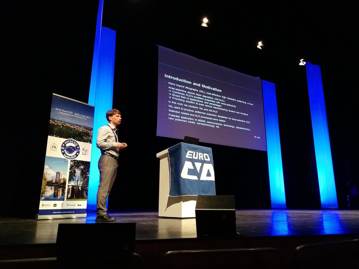
Christoph Hossbach, now at Picosun Germany (a member of ALD Lab Saxony) taking the grand stage presenting on Area Selective ALD (Photo credit: Professor Henrik Pedersen, Twitter)


Marcel Junige (TU Dresden) presenting a poster on ALD Gold precursor candidates (photo credit: Marcel Junige)


Joint exhibition table with Colnatec USA (Wendy Jameson) and VTT Finland (Photo credit: Colin Georgi)


Fraunhofer IKTS (Jonas Sundqvist) presented via video link the latest developments on Hard coatings by CVD and ALD on WC Powder (Photo Credit Jonas Sundqvist)


Advanced Materials Special Issue: Materials Platform at Aalto University

Aalto University Reports (LINK):Advanced Electronic Materials, an academic peer-reviewed high-impact materials science journal, has published a special issue dedicated to materials research at Aalto University, in Espoo (near Helsinki), Finland.


Link to special issue: http://onlinelibrary.wiley.com/doi/10.1002/aelm.201770023/full

Some selected papers interestig for the Atomic Layer Community:

Ozone-Based Atomic Layer Deposition of Al2O3 from Dimethylaluminum Chloride and Its Impact on Silicon Surface Passivation - Yameng Bao,* Mikko Laitinen, Timo Sajavaara, and Hele Savin

Band Bending Engineering at Organic/Inorganic Interfaces Using Organic Self-Assembled Monolayers - Oliver T. Hofmann* and Patrick Rinke

Flexible Thermoelectric ZnO-Organic Superlattices on Cotton Textile Substrates by ALD/MLD - Antti J. Karttunen,* Liisa Sarnes, Riikka Townsend, Jussi Mikkonen, and Maarit Karppinen

Enhanced p-Type Transparent Semiconducting Characteristics for ALD-Grown Mg-Substituted CuCrO2 Thin Films - Tripurari S. Tripathi and Maarit Karppinen*


Wednesday, June 14, 2017

LATE POSTER: 20170614 Process development of ALD and CVD of MoOx and MoS2 employing Mo(CO)6

Here is a LATE POSTER, 20170614 for EuroCVD-BalticALD 2017 in Linköping - Process development of ALD and CVD of MoOx and MoS2 employing Mo(CO)6.


VTT Finland method accelerates the development of microelectronics in three dimensions

Press Release: VTT Technical Research Centre of Finland has developed the unique PillarHall test structures to accelerate the market entry of three-dimensional, small, efficient and low-power but high-performance electronic components. This will benefit developers of challenging thin film and related manufacturing processes, and thereby the entire electronics industry value network.

There has been occasional speculation on whether Moore's Law remains valid. Transistors are already being packed into squares so small that their rate of shrinkage is accelerating in three dimensions. For example, the equivalent of 4 billion 72-storied skyscrapers on a dime has enabled the creation of a 256 GB memory chip.

Picture source VTT Finland Media release.

VTT has developed record-high aspect ratios on an extremely challenging scale (10,000:1 and 100 nm) for the 3D test structures on silicon chips and wafers, to meet the requirements of the most challenging applications. Such applications include in addition to semiconductor circuits, also optics, MEMS, sensors, thin film batteries and photovoltaics.

"What makes our chips special is that we have turned the analysis 90 degrees and adopted a lateral rather than the traditional vertical approach, which enables much faster data production and lead times than current methods. For example, cross-sectional analysis of microscopic vertical structures can take weeks, whereas Pillar Hall provides data without delay. Other advantages include accuracy, versatility and compatibility with varying process conditions," says inventor and Senior Scientist Riikka Puurunen (D.Sc. (Tech.)) of VTT.

The PillarHall test structure also introduces a new parameter space into the analysis, which allows more efficient thin-film R&D, adoption of new industrial applications and process control.

PillarHall is being funded under Tekes' Research Commercialisation Programme. This involves developing silicon chips for quantifying thin-film conformality, which is a key value proposition of ALD (Atomic Layer Deposition) technology. ALD has originally been developed in Finland and Finland's key ALD technology players are involved in the Project Advisory Group: ASM, Beneq, Picosun, the University of Helsinki and Okmetic Oy.

VTT is currently working with PillarHall's 3rd-generation prototypes, which have been successfully tested by Finnish partners and a number of research institutes. VTT is now seeking international partners, in particular, as test users to push forward with the testing and commercialisation of the chips.

"The interest shown by industry and the positive experiences of users build confidence in our vision that PillarHall chips and wafers could one day become the conformality standard and be commercially available," says Project Manager Mikko Utriainen (D.Sc. (Tech.).

More information about the project:

http://pillarhall.com

VTT Blog: Moore's law - is it a spring of productivity? https://vttblog.com/2017/05/30/moores-law-is-it-a-spring-of-productivity/

Day 3 (Tuesday) EuroCVD-Baltic ALD 2017 in Linköping, Sweden

Here is a collection of tweets from Day 3 (Tuesday) EuroCVD-Baltic ALD 2017 in Linköping; Sweden.


Atomic Scale Processing Webinar with Oxford Instruments

Last chance to register! FREE webinar tomorrow:
Atomic Scale Processing | 15th June, 3:30pm BST


In this webinar, our experts Dr Ravi Sundaram and Dr Harm Knoops discuss the processing of atomic scale materials and devices including Graphene and 2D materials, atomic layer etching and atomic layer deposition. The webinar will comprise of two talks, with a Q&A session at the end:

• Atomic scale processing: Atomic Layer Deposition & Etching
Dr Harm Knoops

• Processing of atomic scale materials & devices: Graphene & 2D
materials | Dr Ravi Sundaram


Tuesday, June 13, 2017

Atomic layer deposition for device integration of graphene (Review)

Just published by Prof. Kessels: A brief and easy-to-read synopsis of our new review paper about ALD for device integration of graphene as published in Advanced Materials Interfaces (Atomic Layer Deposition for Graphene Device Integration, 26 May 2017, DOI: 10.1002/admi.201700232).

Atomic Limitts Blog: LINK

Picture from AtomicLimits.com


Day 2 (Monday) EuroCVD-Baltic ALD 2017 in Linköping, Sweden

Here is a collection of tweets from Day 2 (Monday) EuroCVD-Baltic ALD 2017 in Linköping; Sweden.

First invited speaker of Martin Magnusson from on aerotaxy.


Monday, June 12, 2017

Atomic Layer Deposition Market Set to Cross USD 5 Billion by 2022 at a CAGR of 31.27%

According to the new report, “Atomic Layer Deposition Market - By Type (Equipment & Materials); By Application (Gate Dielectrics, Gate Electrodes, Metal Interconnects, Diffusion Barriers, Memory Chips, Multilayer Capacitors, OLED Layers, Solar Cells, Fuel Cells, MEMS and Others); By Geography – Forecast (2016-2022)”, published by IndustryARC, the atomic layer deposition market to cross USD 5 Billion by 2022 at a high CAGR.


Atomic Layer Deposition in increasingly being used in manufacturing of electronic products where thickness of the film is absolutely imperative such as; smart phones, printers, data storage devices, displays, different types of small electronic components and many others products. It is mainly responsible for semiconductor fabrication and nanomaterial synthesis. Growing application of thin film coatings is the major driving factor for atomic layer deposition market. Through atomic layer deposition, ultra-thin films can be created in a sequential and self-limiting way depending on the material or product, which needs the layer to be applied on. Atomic layer Deposition process is especially favored because of its ability to control the film thickness in nanometer thickness regime. Atomic layer deposition is a perfect deposition method for applications where the surface area of the base material is very small.

According to a recent study from IndustryARC the global market value of atomic layer deposition was $910 million in 2015. Atomic layer deposition instruments are expensive as compared to conventional techniques such as MOCVD and PVD, consequently the equipment used for atomic layer deposition accounted for more than 60% of the global market revenue share.

Inquiry before Buying Report @ http://www.industryarc.com/inquiry-before-buying.php?id=15340

Day 1 (Sunday) EuroCVD-Baltic ALD 2017 in Linköping; Sweden

Here is a collection of tweets from Day 1 (Sunday) EuroCVD-Baltic ALD 2017 in Linköping; Sweden.


Thursday, June 8, 2017

Solar conversion of CO2 by ALD modified CuO catalyst


Chemistry World reports that Earth abundant materials can be nano-engineered to make best use of increasingly abundant solar power. Now researchers in Switzerland have developed a catalyst, made entirely from earth abundant materials, that allows solar-generated electricity to reduce the environmental pollutant carbon dioxide to the valuable chemical feedstock carbon monoxide.

In the new research, Luo and colleagues used atomic layer deposition – a modified form of chemical vapour deposition allowing deposition of single, continuous atomic layers – to cover copper oxide nanowires with a very thin layer of tin oxide. Please find more detailed information and sources below

Full story:  LINK

Reference:
M Schreier et al, Nat. Energy, 2017, 2, 17087 (DOI: 10.1038/nenergy.2017.87)

Abstract: The solar-driven electrochemical reduction of CO2 to fuels and chemicals provides a promising way for closing the anthropogenic carbon cycle. However, the lack of selective and Earth-abundant catalysts able to achieve the desired transformation reactions in an aqueous matrix presents a substantial impediment as of today. Here we introduce atomic layer deposition of SnO2 on CuO nanowires as a means for changing the wide product distribution of CuO-derived CO2 reduction electrocatalysts to yield predominantly CO. The activity of this catalyst towards oxygen evolution enables us to use it both as the cathode and anode for complete CO2 electrolysis. In the resulting device, the electrodes are separated by a bipolar membrane, allowing each half-reaction to run in its optimal electrolyte environment. Using a GaInP/GaInAs/Ge photovoltaic we achieve the solar-driven splitting of CO2 into CO and oxygen with a bifunctional, sustainable and all Earth-abundant system at an efficiency of 13.4%.

NC State show ALD enhanced zirconia MOFs for protective clothing against chemical weapons

ScienceDaily reports: Since their first use in World War I and most recently by the Assad regime in Syria, chemical weapons with devastating potential have been developed. Therefore scientists have begun exploring the use of zirconium-based metal-organic framework (MOF) powders to degrade and destroy these harmful compounds.
  • Zirconium Asists in neutralizing toxic materials. 
  • MOF powders are unstable and incorporating them onto clothing has proven challenging. 
Therefore Dennis Lee, Gregory N. Parsons et al has investigated growth of MOFs onto fabric at room temperature, which potentially could realize protection by being coated on to uniforms and other protective clothing.


The researchers developed a process were the a fine fabric (nonwoven) commonly used in reusable shopping bags and some clothing is exposed polypropylene, followed by another exposure to a to a mixture consisting of a zirconium-based MOF, a solvent and two binding agents.

Finally, to make sure that the active zirconia MOF-coating spread evenly across the cloth, they treated the fabrics with thin ALD layers of aluminum, titanium or zinc oxide. They tested this combination with dimethyl 4-nitrophenyl phosphate (DMNP), a relatively harmless molecule that has similar reactivity as sarin, soman and other nerve agents.

They found that the MOF-treated cloths deactivated DMNP (a Sarin like compound) in less than 5 minutes, suggesting this process is a viable means to create improved protective clothing.


References:

American Chemical Society. "New fabric coating could thwart chemical weapons, save lives." ScienceDaily. ScienceDaily, 7 June 2017. www.sciencedaily.com/releases/2017/06/170607123930.htm.

Dennis T. Lee, Junjie Zhao, Gregory W. Peterson, Gregory N. Parsons. Catalytic “MOF-Cloth” Formed via Directed Supramolecular Assembly of UiO-66-NH2 Crystals on Atomic Layer Deposition-Coated Textiles for Rapid Degradation of Chemical Warfare Agent Simulants. Chemistry of Materials, 2017; DOI: 10.1021/acs.chemmater.7b00949

Wednesday, June 7, 2017

Another breakthrough in CMOS-compatible ferroelectric memory

Imec, the world-leading research and innovation hub in nanoelectronics and digital technology, announced today at the 2017 Symposia on VLSI Technology and Circuits the world's first demonstration of a vertically stacked ferroelectric Al doped HfO2 device for NAND applications. Using a new material and a novel architecture, imec has created a non-volatile memory concept with attractive characteristics for power consumption, switching speed, scalability and retention. The achievement shows that ferro-electric memory is a highly promising technology at various points in the memory hierarchy, and as a new technology for storage class memory. Imec will further develop the concept in collaboration with the world's leading producers of memory ICs.

Full story : LINK

Monday, June 5, 2017

IBM, Samsung and Globalfoundries shows off the world´s first 5 nm logic chip with GAAFETs

IBM together with Samsung and Globalfoundries shows off the world´s first 5 nm logic chip with horizontal Gate All Around Field Effect Transistors also referred to as GAAFETs. GAAFETs are a evolutionary development out of FInFETS that were fisrt introduced at 22 nm by Intel. It is predicted that 7 nm will be the last FinFET node and that GAAFETs has to be introduced by then.

Source: IBM LINK

 TEM cross section of 5nm GAAFETs by IBM, Samsung and Globalfoundries (Source IBM)

The GAAFETs are manufactued by deposition stacks of epitaxial silicon and silicon germanium (Si/SiGe Epi). Then by using a combination of EUV lithography and reportedly (LINK) Atomic Layer Etching (ALE) trenches are etched to separate the stack into fins and then afterwards to individual nanowires (or nano sheets as IBM calls them) of Si resp SiGe forming the channels stacked on top of each other. Later the high-k / metal gate (HKMG) stack is deposited in by a sequence of ALD processes conformally covering the nanowire channels.


In the nano sheet FETs, the wires are much wider and thicker presumably giving the nano sheet FETs better electrostatics and drive current

Articles :

Want a smarter phone? IBM and Samsung bring you: Nanosheets!
CNET
If you're frustrated with smartwatches that aren't that smart or phones that don't pack enough power, IBM and Samsung have some good news ...


Sunday, June 4, 2017

EpiValence is sposnoring Best Student Awards at EuroCVD-Baltic ALD 2017 in Sweden

I just a week the EuroCVD-Baltic ALD 2017 conference kicks off in Linköping, Sweden (11-14th of June). Right now many students are putting their final touches to their presentations and posters and to motivate you even more we have a treat for you!


Epivalence is sponsoring the best student poster and best student presentation prices, which will be given at the conference dinner. You can meet Equivalence in the Industry exhibition at the conference.

Thursday, June 1, 2017

Pushing the Bounds of Nanoscale Processing at 'Nanotech 2017: Pushing the Limits' Workshop

Oxford Instruments and the Kavli Nanoscience Institute at the California Institute of Technology (CALTECH) are holding a one day workshop on 19th July 2017.

This workshop will explore recent progress in nanoscale plasma processing research and development, plus looking at future trends in the fabrication and application of micro, nano and atomic scale structures and devices.

Source: AZoNano LINK