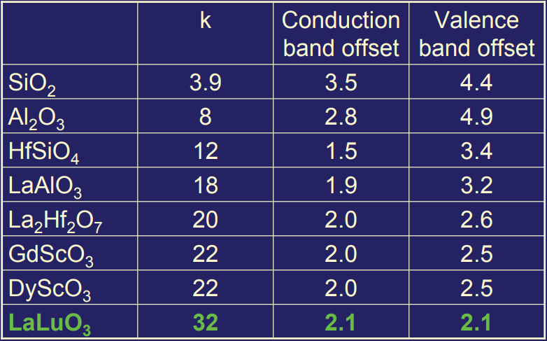
Thursday, January 24, 2019

Volkswagen invests USD 10 M in US ALD start-up Forge Nano for battery material research

The Volkswagen Group is investing US$10 million in the start-up Forge Nano Inc with a view to reinforcing its specialist knowledge in the field of battery research. Forge Nano is investigating a material coating technology that could further improve the performance of battery materials. As a partner, Volkswagen will provide support for industrial trials of this technology. The transaction is still subject to approval by the authorities. 

(forgenano.com)

Volkswagen has been collaborating with Forge Nano on advanced battery material research since 2014. The startup with headquarters in Louisville, Colorado, is investigating processes for scaling atomic layer deposition (ALD) to create new core-shell materials, especially for battery applications. ALD is a chemical process for applying atomic scale coatings one atom at a time. With its specific ALD technology, Forge Nano aims to boost energy density of vehicle battery cells.
For example, a higher energy density would have positive effects on the range of electric vehicles. Volkswagen has been lending their automotive and battery expertise towards Forge Nano’s applied research efforts.

The Volkswagen Group is consistently forging ahead with its electric offensive and intends to offer more than 50 battery-electric models by 2025, accounting for about a fifth of its entire model portfolio. To safeguard this approach, Volkswagen is cooperating with strategic battery cell suppliers and developing its own specialist know-how in battery research. This also includes targeted venture investments. Volkswagen is increasingly investing in international start-ups to bring innovative technologies forward to production maturity together.

Dr. Axel Heinrich, Head of Volkswagen Group Research, said: “At Volkswagen, we want to be the world’s leading provider of e-mobility. We are continually expanding the battery technology know-how required for this purpose. We need to safeguard our technological competence for the future. Cooperation with start-ups is a key element in these efforts. We are acting as a partner to Forge Nano and intend to provide the team with opportunities to carry out industrial trials with its innovative technology.”

Dr. Paul Lichty, Founder and CEO of Forge Nano, said: “Our atomically precise surface engineering technology is ushering in a new era of high performance materials. We are excited to partner with a company that has such a strong commitment to commercializing innovation.”

Wednesday, January 23, 2019

ASM International enhances ALD productivity with new 300 mm XP8 Quad Chamber Module

ASM International enhances ALD productivity with new very competetive 300 mm XP8 Quad Chamber Module providing:
  • High productivity platform for PEALD and PECVD Processing of up to 16 wafers at a time.
  • Integrated processing using both the "old" Double (DCM) and new Quad Chamber Modules (QCM) for flexibility and productivity optimization.
  • Earlier in 2018 ASM relaunched the two industry ALD workhorse chambers, Pulsar Thermal ALD and Emerald PEALD used for e.g. HKMG,  as Double module on XP8 - this now means that all ASM ALD and PEALD chambers can be used on the high productivity platfrom XP8 eilter sa DCM or QCM or both.
[ASM News, LINK] ASM International N.V. (Euronext Amsterdam: ASM) today introduced its XP8 QCM tool for high-productivity 300mm single-wafer plasma enhanced atomic layer deposition (PEALD) and plasma enhanced chemical vapor deposition (PECVD) applications. The QCM, or Quad Chamber Module, is a process module with four tightly integrated process reactors. Up to four QCM modules can be configured to each XP8 platform, enabling processing of up to 16 wafers at a time. 
Quad chamber modules (QCMs) 30, 32, 34, and 36 are connected to four side surfaces of the vacuum chamber 22. Each QCM is a module having four reactor chambers (RC1 to RC4). Processing such as plasma film forming processing is performed on a substrate in each reactor chamber. (ASM Patent application US20170278074A1)
"Across the board, customers are requiring increased throughput" said Tominori Yoshida, ASM's General Manager and Senior Vice President, Plasma Products Business Unit. "The XP8 QCM addresses advanced PEALD and PECVD films including silicon oxide for multiple patterning and silicon nitride for other applications, and relatively thick films where the tool's architecture enables higher throughput compared to other single-wafer configurations."

The new reactor architecture is well-suited for high-volume advanced-node memory and logic applications, which require the precise film control provided by the QCM's innovative reaction chamber. The QCM chambers use the same advanced reactor technology as ASM's original PEALD and PECVD XP8 Dual Chamber Modules (DCMs). Hundreds of these DCMs have been running for years in high-volume production globally at key logic, foundry and memory customers. This allows customers to easily transfer existing processes to the new QCM chamber. As a result, the XP8 QCM tool is already in high-volume manufacturing at multiple customers worldwide.

Furthermore, the XP8 architecture enables integrated processing using both DCMs and QCMs for flexibility and productivity optimization.

Strem Chemicals’ offers new La-FMD ALD precursor for future leading edge logic and memory products

Strem Chemicals’ offering of La-FMD is one of the most promising metal-amidinate ALD precursors for lanthanum (La) based ALD thin-films which are potentially strong candidates for high-k gate dielectric in the next generation of CMOS technology.

Rare earth elements have entered high volume manufacturing for advanced logic devices since the 32 nm node (IBM, Samsung and Globalfoundries – Chipworks 2010). Especially for Lanthanum (La) — the eponym of the lanthanide series in the periodic table has been implemented as a dopant in the high-k metal gate stack. Lanthanum oxide (La2O3, dielectric constant ~ 27), for example, has been explored for two decades as a high-k gate dielectric for the replacement of conventional silicon dioxide (SiO2) gate dielectric in the next generation transistors in logic as well as in dynamic random access memories (DRAMs).
Keyword segmentation of patent applications the last 20 years for Lanthanum and “Atomic Layer Deposition” [Patbase search 15 November 2018]

Atomic layer deposition is the most promising method for growing ultra-thin-films of La based gate dielectrics and has therefore been under extensive research and filing of patent applications in the last 20 years. The R&D effort has been focused on fields relating to dielectric and high-k dielectric applications in the semiconductor industry (see keyword segmentation above). The atomic layer-by-layer film growth facilitated by self-limiting surface reactions in ALD provides atomically precise film-thickness control, good uniformity across a large area substrate, and excellent conformality in case of high aspect ratio structures like modern FinFETs and memory capacitor type pillar structures. However, to work flawlessly it requires the ALD precursors that have specific properties (LINK): 

1. Sufficiently volatile (at least ~ 0.1 Torr equilibrium vapor pressure at a temperature at which they do not decompose thermally).

2. Rapidly vaporizing and at a reproducible rate (conditions that are usually met for liquid precursors, but not for solids).

3. Not self-reacting or decomposing on the surface or in the gas phase (for self-terminating surface reactions).

4. Highly reactive with the other reactant previously attached to the surface, which results in relatively fast kinetics and thus lower ALD temperatures and cycle times.

5. Volatile byproducts that can be easily purged in order to prepare for the subsequent half-cycle.

6. Non-corrosive byproducts to prevent non-uniformities due to film etching and corrosion of the tool.
In 2007, Intel Corporation incorporated HfO2 into high-k gate dielectric stack at 45 nm technology node. However, pure HfO2 suffers from low-k interface layer problem with Si, limiting lower equivalent oxide thickness (EOT) values. It also readily crystallizes at temperatures as low as ~500°C. Therefore, amorphous dielectrics with high thermal stability are still sought after for no intrinsic defects (e.g. grain boundaries), provided they still offer the advantages of HfO2, such as high dielectric constant, wide band-gap, and low leakage current. Lanthanum-based ternary oxides, such as lanthanum scandate (LaScO3) and lanthanum lutetium oxide (LaLuO3), deposited by ALD process involving metal amidinate precursors reportedly exhibit desirable structural and electrical properties. In fact LaLuO3 is potentially the best amorphous phase gate dielectric with dielectric constant k~32. It doesn’t form low-k interfacial layers with Si which enables effective oxide thickness (EOT) values < 1 nm with significantly low leakage current. Another factor contributing to the low leakage current across ALD grown thin LaLuO3 gate dielectric is the large band-offset (2.1 eV) with respect to Si; the symmetric conduction and valence band offsets result into equal leakage currents in electron driven NMOSFETs and hole driven PMOSFETs. It stays amorphous and doesn’t form alloys with Si or Ge after respective source/drain activation anneals.  


As a very recent example of an actual high aspect ratio application on 300 mm wafers requiring all ALD precursor characteristics described above (1 to 6) we can see the paper that Imec presented at this famous IEDM conference, on using a LaSiOx layer as a dipole inserted in the HKMG stack. Imec succeeded in stacking the complete FinFET front end module on top of a "standard" bulk silicon FinFET module demonstrating also good threshold voltage tuning, reliability and low-temperature performance. Presumably it has most likely been deposited by an ALD process since it will have to conformally coat the fins and ensure precise thickness control and uniformity : IEDM2018 Paper #7.1, “First Demonstration of 3D Stacked FinFETs at a 45nm Fin Pitch and 110nm Gate Pitch Technology on 300mm Wafers,” A. Vandooren et al, Imec [LINK].
As in this case and many more, the stringent qualifications for ALD precursors put them in the category of high quality specialty chemicals — the performance or function specific materials or molecules of choice. The deposited film properties are strongly influenced by the physical and chemical properties of a single molecule or a formulated mixture of molecules as well as its chemical composition. Therefore, it puts a lot of pressure on the manufacturer and supplier of the high purity specialty chemicals in terms of quality, purity, documentation procedures, customer service etc.

Friday, January 18, 2019

ULVAC Inc. and Oxford Instruments Plasma Technology collaborate to bring Atomic Scale Processing solutions to the Japanese Power and RF markets

 
[Oxford Instruments, LINK] Leading semiconductor equipment solution providers, Oxford Instruments Plasma Technology (a trading name of Oxford Instruments Nanotechnology Tools Limited, Tubney, Oxford, UK) and ULVAC Inc., (Chigasaki, Kanagawa, Japan) are delighted to announce a key collaboration which will bring leading edge deposition and etch technology solutions to GaN and SiC based Wide Band Gap production customers in Japan.

“Oxford Instruments Plasma Technology is excited to be collaborating with ULVAC in order to bring its proven process solutions to the Japanese power and RF markets”, commented Mike Gansser-Potts, Managing Director, Oxford Instruments Plasma Technology. “This relationship, which will begin with ULVAC as our channel partner in Japan, will allow local production customers access to Oxford Instruments’ suite of Atomic Scale Processing solutions”

“This is indeed a very significant collaboration”, confirmed Tetsuya Shimada, General Manager for Advanced Electronics Equipment Division of ULVAC Inc., “Our new collaborator, Oxford Instruments Plasma Technology, has critical process technology and know-how which complements our own capabilities. Combined with our customer support infrastructure this will allow us to provide a complete solution to our Japanese customers.”

Oxford Instruments Plasma Technology’s Atomic Layer Deposition (ALD) and Atomic Layer Etch (ALE) are critical process steps for GaN and SiC based devices to enable functionality and reliable device manufacturing. With the critical know-how and expertise gained over the last ten years in Wide Band Gap applications, Oxford Instruments Plasma Technology is perfectly placed to serve the technology leading Japanese production customers in these markets.

Wednesday, January 16, 2019

Come to Berlin for the EFDS ALD for Industry - 3rd Workshop and Tutorial, March 19-20, 2019

Including Industrial Exhibition and Practical ALD Show

A topical workshop with focus on industrialization and commercialization of ALD for current and emerging market

Atomic Layer Deposition (ALD) is used to deposit ultraconformal thin films with sub-nm film thickness control. The method is unique in the sense that it employs sequential self-limiting surface reactions for growth in the monolayer thickness regime. Today, ALD is a key technology in leading semiconductor technology and the field of application in other leading-edge industries is increasing rapidly. According to market estimates the equipment market alone is currently at an annual revenue of US$ 1.5-1.7 billion (2017) and it is expected to double in the next 4-5 years.

In a European context ALD was invented independently twice in Europe (Russia & Finland) and since the last 15 years Germany has grown to become one of the strongest European markets for ALD in R&D, chemicals, equipment and end users.

The Event will focus on the current markets for ALD and addresses the applications in semiconductor industry, MEMS & Sensors, Battery Technology, Medical, Display, Lightning, Barriers and Photovoltaics.


Tuesday, January 15, 2019

CALL FOR PAPERS - 4th Area Selective Deposition (ASD) Workshop will be held on April 4th – 5th, 2019 in IMEC, Leuven (Belgium)


 Visit our website:

ASM and IMEC are proud to announce that the 4th Area Selective Deposition (ASD) Workshop will be held on April 4th – 5th, 2019 in IMEC, Leuven (Belgium).

This workshop will bring together leading experts from both academia and industry to share their vision and results on ASD. Based on a series of successful workshops at the: North Carolina State University in 2018, Eindhoven University of Technology in 2017 and IMEC in 2016, the two-days program will include invited and contributed speakers, a poster session and a reception on the evening of April 4th.

The workshop will cover a wide range of topics, including the following:

Area selective epitaxy and area selective chemical vapor deposition: processes and mechanisms, defects control

Intrinsic selectivity of ALD processes: nucleation and interface studies, chemical selectivity in surface reactions, competitive adsorption, precursors design, modeling of surface reactions

Methods for area selective activation / deactivation: use of inhibitors (self-assembled monolayers, polymers), plasma-/beam-induced activation

Processes and mechanisms for area selective atomic layer deposition: deposition of metals or dielectrics, thermal/plasma enhanced ALD, 3D or patterned substrates, substrates preparation, sequential deposition/etching,

Metrology and defects control:
surface characterization techniques, selective etching of defects

Applications of area selective deposition:
semiconductor industry (integration needs of device makers, solutions proposed by the equipment makers), catalysis, energy generation and storage, etc.

On behalf of the organizing committee, it will be our pleasure to welcome you in Leuven.

Andrea Illiberi

Program chair of the 4th ASD workshop

Thursday, January 10, 2019

Workshop, Tutorial & Practical Show „ALD for Industry“, 19. – 20. März 2019, Berlin


ALD – eine vielversprechende Technologie

Die Atomlagenabscheidung (ALD) verspricht mit ihrem besonderen Ansatz, Beschichtungen Lage für Lage geordnet abzuscheiden, zahlreiche Vorteile und Möglichkeiten. 2019 treffen wir uns nunmehr zum dritten Mal mit zunehmendem Teilnehmerkreis, um das Potential der Technologie und die aktuellen Fortschritte aufzuzeigen und zu diskutieren. In diesem Jahr stehen neben interessanten Vorträgen vor allem Praxistipps im Vordergrund. In der „Practical ALD Show“ geben Experten Tipps zur Durchführung und Prozessoptimierung. Einzelne Ausstellungs-Restplätze für Sponsoren sind noch buchbar.


Das Jahrestreffen der Plasma- und Vakuumexperten – V2019 + ALD


Das Jahrestreffen der Plasma- und Vakuumexperten – V2019

+ ALD (Vorlesung, Poster, Workshop)

Die Vorbereitungen laufen auf Hochtouren. Die V2019 wird in diesem Jahr wieder zahlreiche Experten, Anbieter, Nachwuchskräfte und Interessierte zur Vakuum- und Plasmaoberflächentechnik zusammenführen. Diesmal findet das Event in der Saalebene des Internationalen Congress Center Dresden (ICD) statt – welches gleich an die historischen, barocken Bauwerke der Altstadt anschließt. Die diesjährige V verbindet Bewährtes und Neues. Da sind neben Vorträgen und Fachgesprächen die zahlreichen Industrieaussteller aber auch neue Workshop-Themen, ein Fachkräfte-Scouting und Firmenbesichtigungen zu erleben. Seien Sie beim Branchentreff dabei. Zahlreiche Aussteller haben bereits Ihren Stand gebucht. 

Sichern Sie sich rechtzeitig Ihre repräsentative Ausstellungsfläche.