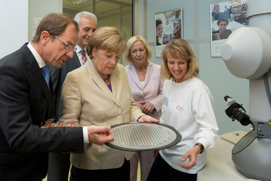
Showing posts with label Semiconductor. Show all posts

Saturday, July 18, 2015

Growth forecast for Wafer Fab Equipment and ALD according to Gartner

Good news of ALD - Gartner has forecasted a growth for the Advanced nodes to come!

Gartner says that the Worldwide semiconductor revenue is forecast to reach $348 billion in 2015, a 2.2 percent increase from 2014, but down from the previous quarter's forecast of 4.0 percent growth, according to Gartner, Inc.


Growth forecast for Wafer Fab Equipment according to Gartner (Graph from ASMi Investor Technology Seminar at SEMICON West)


"The outlook for the major applications that drive the semiconductor market, including PCs, smartphones, and tablets, have all been revised downward. This, combined with the impact of the strong dollar on demand in key markets, has resulted in a lower semiconductor forecast for 2015," said Jon Erensen, research director at Gartner. "The typical second-quarter bounce did not materialize this year, and as a result, the semiconductor industry is more back-end loaded and dependent on a strong third-quarter rebound, driven by Windows 10 and the ramp-up to the holiday season.” 

From an application point of view, smartphones and solid-state drives (SSDs) will continue to drive semiconductor market growth, while the traditional PC segment will experience the greatest decline, with production units down 8.7 percent in 2015, slightly weaker than the previous quarter's forecast. "Inventory in the PC market remains high despite vendors looking to clear the supply chain in anticipation of Windows 10 and Intel's Skylake products. Any issues with the launches of Windows 10 or Skylake in the third quarter of 2015, which are expected to reinvigorate PC sales, could lead to further decline," said Mr. Erensen.

In the smartphone market, Apple's iPhone is the bright spot for the market with strong unit growth and increasing average selling prices (ASPs), driven by the strong performance of the iPhone 6 and iPhone 6 Plus. However, lackluster performance in high-end Android smartphones and general softness in the smartphone market in China will continue to impact growth.

Although the wearables market, including smartwatches, head-mounted displays (HMDs), smart glasses and Bluetooth headsets, is a growing industry, revenue for wearables semiconductors — processing, sensing and communications chips — will represent only 1 percent of total semiconductor revenue by 2019. Smartwatches are the top semiconductor growth in the near term.

From a device point of view, DRAM continues to be one of the primary growth drivers of the overall industry. DRAM revenue is expected to increase 3.8 percent in 2015, following a 32 percent increase in 2014. However, Gartner expects an oversupply (or "underdemand") to develop in 2016 as limited new capacity comes online and technology migration continues. DRAM industry revenue is expected to decline 17.4 percent in 2016 and 7 percent in 2017.

"The typical second-quarter bounce did not materialize this year, and as a result, the semiconductor industry is more back-end loaded and dependent on a strong third-quarter rebound, driven by Windows 10 and the ramp-up to the holiday season," said Mr. Erensen.

Tuesday, July 14, 2015

Germany to fund the Semiconductor industry with 400 milion Euro

"Every second chip made in Europe comes from Saxony!"

Happy days in Dresden, Silicon Saxony and Germany today - Yesterday Globalfoundries announced that they are investing in Fab 1 in Dresden to ramp 22 nm FD-SOI and today Angela Merkel and Johanna Wanka comes for a visit to Dresden and promises 400 million Euro support package until 2020 for the semiconductor industry!


"Um Innovationen in der Halbleiterindustrie auch künftig voranzutreiben, erarbeitet das Bundesforschungsministerium bis Ende des Jahres zusammen mit weiteren Ressorts ein neues Rahmenprogramm. Das Programm soll mit einem Volumen von 400 Millionen Euro bis 2020 ausgestattet werden. Das hat Bundesforschungsministerin Wanka bei ihrem Besuch in Dresden angekündigt. " - http://www.bmbf.de/de/28961.php

Chancellor Angela Merkel entering the helicopter in Berlin to fly 200 km south to Dresden. (Twitter, BMBF)


Rutger Wijburg (VP and General Manager Fab1, Dresden) explains factory physics for Sanjay Jha (CEO Globalfoundries) Chancellor Angela Merkel, Ministerpräsident Stanislaw Tillich and Bundesforschungsministerin Johanna Wanka using a model Globalfoundries Fab 1 in Dresden. (Photo: Heiko Weckbrodt)

More details for those of you reading German can be found in the excellent coverage by Heiko Weckbrodt :

Bund sagt 400 Millionen € für Mikroelektronik zu

Kanzlerin Merkel debattiert in Dresden Mikroelektronik-Strategie

MDR Sachsen Video in German:

Overview
http://www.mdr.de/sachsenspiegel/video284012.html

Silicon Saxony
http://www.mdr.de/sachsenspiegel/video284020.html

Globalfoundries
http://www.mdr.de/sachsenspiegel/video283788.html


Later Frau Bundeskanzlerin Dr Merkel also stopped by Fraunhofer to meet with The Fraunhofer President Prof. Dr. Reimund Neugebauer.


Angela Merkel also visited Infineon’s Dresden 300 and 200 mm fabs today and discussed the political framework for a competitive development and production in Germany with CEO Reinhard Ploss. - See more at: http://www.electronicsweekly.com/news/business/merkel-visits-infineon-dresden-fab-2015-07/#sthash.XHTLv12Y.dpuf


Yesterday, flanked by two clean room engineers posing with 300 mm device wafers the Globalfoundries Managers Gregg Bartlett, Sanjay Jha (CEO) und Rutger Wijburg (VP and General Manager Fab1, Dresden) announce that Globalfoundries will invest $250 million for 22nm FD-SOI production in Fab 1 Dresden, Germany. From the press conference in Dresden (photo by Heiko Weckbrodt, www.computer-oiger.de)

Friday, June 26, 2015

Research and Markets: 2015 ALD/CVD High K and Metal Precursors for the Semiconductor IC Market

Pretty impressive to know that "The semiconductor CVD/ALD industry utilizes precursors for over 29 different metals and metal oxides provided globally by 23 suppliers." Thanks Rob for sharing this one in the ALD LinkedIn Group!

Research and Markets has announced the addition of the "2015 ALD/CVD High K and Metal Precursors for the Semiconductor IC Market" report to their offering.

The High K / ALD Precursors report provides information on the applications and markets associated with front end and back end of line precursors used to produce high dielectric constant (K) dielectrics and atomic layer deposition dielectrics and metals. Market size, growth, and market share statistics are provided.

Rancho Santa Fe, CA, June 15: Use of front-end Ta and W metal gate and Hf gate dielectric precursors will grow over 2.5x by 2020, according to a new report from this research industry, 2015ALD/CVD High K and Metal Precursors for the Semiconductor IC Market. The overall precursor market sits at $185M today, and is expected to grow 18% over the next five years. The advanced metal gate and gate dielectric segments within that market are expected to grow at 168%, more than compensating for the 25% decline anticipated for the high memory precursor segment.

The 2014 market size for CVD/ALD precursors for interconnect applications was approximately $93M, up 19% over 2013. 2015 is forecast to be up another 15%. By 2016, growth in this segment will be dominated by cobalt barrier precursors, as WF for contact and plug applications begins to decline. The 5-year CAGR for this area is forecast to be 9.4% overall.

The precursor market for capacitor CVD/ALD applications, which includes DRAM and a variety of memory devices, is expected to be flat for the next 5 years, fluctuating in the range of $55M to $70M. The difficulties in forecasting conventional memory demand are compounded by the emergence of a host of new memory device structures, not all of which depend on these materials.

The semiconductor CVD/ALD industry utilizes precursors for over 29 different metals and metal oxides provided globally by 23 suppliers. In addition to market analysis, process flow details, precursor candidates and critical supply chain issues, the report includes regional ranking for major suppliers of vapor deposition precursors.

Tuesday, June 16, 2015

JUST RELEASED - TEHCHET's 2015 Materials Market and Business Trends, Supply Chain Reports

IoT is growing those materials considered trailing edge. 3D devices is driving growth on the front end. Enabling packaging technologies paving the way for mid-high end device connectivity. Gases, Targets, CMP Consumables, WLP Polymers and Silicon Wafers Reports just released.


Sunday, May 31, 2015

Epitaxial growth of GaN nanowires on metallic TiN by Paul-Drude-Institut, Berlin

Paul-Drude-Institut für Festkörperelektronik in Berlin has recently published a paper (below) on how to grow GaN Nanowires on TiN. From a silicon based semiconductor device perspective this is very interesting results since TiN can be used to make ohmic contact to silicon. For instance the is used in most DRAM Capacitor cells today where the word line is connected by a TiN/Ti/TiSi/Si ohmic contact. This technology was invented by Qimonda - The buried Word Line technology that was introduced at 65 nm and has been transferred to many other companies since then (Winbond, Micron, Elpida, ...). Or as the researchers at the Paul-Drude-Institut states:  

"The freedom to employ metallic substrates for the epitaxial growth of semiconductor nanowires in high structural quality may enable novel applications that benefit from the associated high thermal and electrical conductivity as well as optical reflectivity."


Epitaxial Growth of GaN Nanowires with High Structural Perfection on a Metallic TiN Film 

M. Wölz , C. Hauswald , T. Flissikowski , T. Gotschke , S. Fernández-Garrido , O. Brandt , H. T. Grahn , L. Geelhaar *, and H. Riechert 
Nano Lett., Article ASAP DOI: 10.1021/acs.nanolett.5b00251 
Publication Date (Web): May 22, 2015


Vertical GaN nanowires are grown in a self-induced way on a sputtered Ti film by plasma-assisted molecular beam epitaxy. Both in situ electron diffraction and ex situ ellipsometry show that Ti is converted to TiN upon exposure of the surface to the N plasma. In addition, the ellipsometric data demonstrate this TiN film to be metallic. The diffraction data evidence that the GaN nanowires have a strict epitaxial relationship to this film. Photoluminescence spectroscopy of the GaN nanowires shows excitonic transitions virtually identical in spectral position, line width, and decay time to those of state-of-the-art GaN nanowires grown on Si. Therefore, the crystalline quality of the GaN nanowires grown on metallic TiN and on Si is equivalent. The freedom to employ metallic substrates for the epitaxial growth of semiconductor nanowires in high structural quality may enable novel applications that benefit from the associated high thermal and electrical conductivity as well as optical reflectivity.

Saturday, March 1, 2014

Atomic Layer Deposition engineers met in San Diego during SEMATECH’s Q1 Manufacturing Week 17-20th Feb

As reported earlier here on the ALD News Blog, Atomic Layer Deposition engineers met in San Diego during SEMATECH’s Q1 Manufacturing Week to benchmark ASM, TEL, HKE, AMAT and JUSUNG equipment productivity and to share some best known methods from the HVM Fabs. Samsung, tsmc, Intel, GLOBALFOUNDRIES, IBM, UMC, Winbond, HP and Freescale engineers all participated. The topics of key interest are:

1) Cost of precursor and dry-precursor usage – taring the weight of dry precursors is not fail safe and therefore not HVM friendly

2) Cost savings were identified of $800K per tool per year

3) Some OEM equipment still not being HVM friendly even after 10 years of ALD in manufacturing (HVM hardening & readiness is low compared to other equipment types)

4) FDC approaches and data collection frequencies (looking at 10Hz for metal ALD right now but potentially requiring 100Hz moving forward)

5) Trap installation, Helium de-gassers and special fore-line consideration


Boyd Finlay project manager from Manufacturing Technology at SEMATECH in Albany together with ALD Equipment Engineers and Experts from the top Leading Edge Fabs. 

 
Atomic Layer Deposition engineers from Samsung, tsmc, Intel, GLOBALFOUNDRIES, IBM, UMC, Winbond, HP and Freescale engineers all participated in the meeting.

GlobalFoundries and Fraunhofer IIS to collaborate on EUROPRACTICE, Europe’s MPW wafer shuttle program

Press release
GLOBALFOUNDRIES and Fraunhofer Institute for Integrated Circuits IIS today announced the extension of their long-term collaboration, focusing on 40nm and 28nm processes. GLOBALFOUNDRIES will also join the European Multi Product Wafer (MPW) Program EUROPRACTICE.


Through the collaboration GLOBALFOUNDRIES will offer its leading-edge foundry capabilities to Fraunhofer IIS as an aggregator, and Fraunhofer will enable the academic network in Europe to get access to GLOBALFOUNDRIES’ process technologies and Process Design Kits (PDK) via EUROPRACTICE.

“As one of the largest foundries worldwide and the largest wafer manufacturer in Europe we are proud to enter this prestigious program,” said Karl Lange, GLOBALFOUNDRIES Vice President of Sales for Europe. “With Fraunhofer as channel partner, combined with our broad technology portfolio and process know-how, we will add significant value to EUROPRACTICE.”
 

“The offer of GLOBALFOUNDRIES technologies down to 28nm to Europe’s universities and research institutes is an important step for EUROPRACTICE and will stimulate education and research in IC design,” said Josef Sauerer, Head of the Integrated Circuits and Systems Department at Fraunhofer IIS. “Also, our contract research with industries will benefit from GLOBALFOUNDRIES’ advanced technology portfolio”

Fraunhofer IIS and GLOBALFOUNDRIES started their collaboration in 2004 with the successful launch of 180nm and later 55nm programs. The extended collaboration will introduce technology nodes down to 28nm in the European Wafer Shuttle Program, helping European academia and research institutes to get access and support for CAD tools and ASIC prototyping at reduced costs.

Sunday, February 23, 2014

The Hafnium FET - Your kids will love this video!

Dad, what do you do at work? The answer is finally here - The Hafnium FET - Your kids will love this video!


Friday, February 21, 2014

HfO2 still going strong for Post-Silicon Channel Materials

According to a recent article HfO2 still going strong for Post-Silicon Channel Materials!
 
"Once device-grade channel materials are achieved, formation of a high quality gate dielectric is the next step. Here, recent results offer reason for optimism. As previously discussed, an initial Al2O3 deposition does not appear to be needed to passivate the InGaAs interface. While a clean surface is essential for successful gate oxide deposition, and atomic layer deposition appears to be an enabling technology for surface preparation, D. Hassan Zadeh and coworkers also obtained good results with La2O3 dielectrics. This material, along with HfO2, offers much a higher dielectric constant than Al2O3, improving ultimate scalability of alternative channel devices."
 
 
Read all about it on "New Challenges For Post-Silicon Channel Materials", by Katherine Derbyshire, Semiconductor Engineering: http://semiengineering.com/next-steps-for-post-silicon-channel-materials/

As reported by CompoundSemiconductor, Engineers from MIT are claiming to have fabricated the first tunnel FET with a double quantum well InGaAs/GaAsSb structure. This work has been published in: IEEE Electron Dev. Lett. 34 1503 (2013). MIT demonstrate employing HfO2 high-k on an InGaAs channel.


Engineers from MIT have fabricated a double quantum well FET (a). Cross-sectional tunnelling electron microscopy provides images of the tunnelling junction and gate stack in the gated region (b), and the edge of the InGaAs air bridge (c). A top view of the air-bridge, after suspension, is provided by a scanning tunnelling microscope (d) [as reported by CompondSemiconductor.net].

Tuesday, February 18, 2014

Samsung 3D-VNAND Promo Video and scaling in 3D

Samsung has been mass-producing 3D NAND modules since August last year according to this source. Here is a most informative news on Samsung 3D-VNAND technology from iTers News discussing limits to 2D scaling beyond 10 nm and "3D scaling".


Here is a interesting presentation from Applied Materials on 3D NAND "Winning in 3D NAND" explaining quite some details on process requirements for going from 2D to 3D technology.
 

"Advantage of 3D NAND is that it doesn’t require leading-edge lithography…the burden will shift from lithography to deposition and etch."  Ritu Shrivastava, VP Technology, SanDisk, May 2013 (SemiMD) [Picture is a screenshot from Applied Materials presentation linked above]

Sunday, February 2, 2014

IBIS predict that cost/gate is now increasing and thus is no longer an economic driver to move to the next node


At a Semi Industry Strategy Symp (ISS) Int Business Strategies (IBS) presented a forecast for the semiconductor industry until 2020. i-Micronews reports on this event here.

"IBIS predict that cost/gate is now increasing and thus is no longer an economic driver (for same wafer size) to move to the next node."


Interesting graph that shows that 28nm is the cheapest node ever (per gate) and will probably stay so unless 450mm wafers will make a difference. As we all know 450mm has been delayed again, meaning 28nm will probably be the dominating node for a long time to come.

The IBIS report concludes:

"IBIS further predicts that:
- 28nm will have long lifetime ( Probability 80% )
- 20nm yields will improve, and will be high volume technology node in 2015 and 2016 (Probability 50%)
- 16/14nm will provide low cost gates and support high bandwidth interfaces in SoC environment (Probability 20% in 2016 and 50% in 2017)
- 10nm will likely be postponed, cost per gate will be prohibitive and unclear as to demand other than high speed processors and FPGAs (Probability 90%)."

According to IC Insights’ ranking of the leading IC foundries, "... the top 13 foundries in the figure represented 91% of total foundry sales in 2013. For comparison, the leading 13 foundries accounted for 84% of total foundry marketshare in 2009, the year before Samsung dramatically ramped up its IC foundry production for Apple."