Showing posts with label Applied Materials. Show all posts

Thursday, October 31, 2019

ASM International settles with Kokusai for Batch ALD patent licenses (US$61 million)

October 29, 2019, 12.15 p.m. CET (LINK) ASM International N.V. (Euronext Amsterdam: ASM) today announces that it has entered into a settlement agreement with Kokusai Electric Corporation (formerly known as Hitachi Kokusai Electric Inc. and hereinafter referred to as “KEC”) to resolve the arbitration proceeding relating to the license agreement which expired in November 2017. As part of this settlement, KEC will pay ASM an amount of US$61 million. With this settlement all pending disputes between ASM and KEC with respect to patent licenses have been resolved.

As announced on February 23, 2018, ASM initiated an arbitration proceeding on August 30, 2017 with the American Arbitration Association against KEC for breach of the license agreement between the companies. This license agreement provided KEC and its affiliates a license under certain patents of ASM in the field of Batch ALD. The companies have now entered into a settlement agreement concerning all the matters of the arbitration.

This arbitration settlement is separate from the settlement of all patent lawsuits and invalidation proceedings between ASM and KEC that was announced on July 1, 2019.

The settlement of the arbitration will positively impact ASMI’s sales and bookings in Q4 2019 with an amount of US$61 million, or approximately €56 million.
 
Background:

- Applied Materials to buy Japan's Kokusai to boost memory chip business and ALD (LINK)

- ASM International settles (US$115 million) with Kokusai Electric Corporation on the use and infringement of ALD patents  (LINK)


Thursday, July 4, 2019

Integrated Process Monitoring for New Memories (MRAM, PCRAM, ReRAM) by Applied Materials

[Applied Materials] For new memories to reach high-volume manufacturing, the industry must enable new process control solutions says Applied’s Niranjan Khasgiwale. Read his latest blog to find out what’s driving the need for new metrology techniques.

Applied Materials: LINK 


Monday, July 1, 2019

Applied Materials to Acquire Kokusai Electric and enter the Large Batch CVD and ALD market

SANTA CLARA, Calif., July 01, 2019 (GLOBE NEWSWIRE) -- Applied Materials, Inc. (“Applied”) (Nasdaq: AMAT) today announced a definitive agreement under which Applied will acquire all outstanding shares of Kokusai Electric Corporation (“Kokusai Electric”) for $2.2 billion in cash from global investment firm KKR.

Kokusai Electric is a leading company in providing high-productivity batch processing systems and services for memory, foundry and logic customers. These systems complement Applied’s leadership portfolio in single-wafer processing systems. Kokusai Electric has strong customer relationships, world-class supply chain and manufacturing capabilities in Japan and Asia, and a talented team of employees.

Following the close of the transaction, Kokusai Electric will operate as a business unit of Applied’s Semiconductor Products Group and continue to be based in Tokyo, with technology and manufacturing centers in Toyama, Japan and Cheonan, Korea. The acquisition is expected to be immediately accretive to Applied’s non-GAAP earnings per share at close.

The transaction has been approved by the Applied Materials Board of Directors. The transaction is expected to close within approximately 12 months and is subject to regulatory approvals and other customary closing conditions.

“Kokusai Electric has a strong culture of innovation along with excellent customer relationships and serves fast-growing areas of the wafer fab equipment market,” said Gary Dickerson, president and CEO of Applied Materials. “By bringing Kokusai Electric’s talented team into Applied, we believe we will accelerate innovation for customers and create significant value for our shareholders.”

“The opportunity to combine with Applied Materials will be very attractive for Kokusai Electric’s customers and employees alike,” said Fumiyuki Kanai, president and CEO of Kokusai Electric. “We are excited about the opportunity to integrate Kokusai Electric’s experienced team with Applied’s global development, customer support and services capabilities. We believe the combination will accelerate our ability to bring exciting new technologies to customers.”

Applied expects to finance the transaction using a combination of balance sheet cash and a term loan facility. Following the close of the transaction, the company will prioritize repayment of the term loan balance while maintaining its long-term commitment to return cash to shareholders through dividends and share repurchases.

Goldman Sachs & Co. LLC served as exclusive financial advisor, and Hogan Lovells and Cleary Gottlieb Steen & Hamilton LLP served as legal counsel for Applied Materials.

Conference Call and Webcast

Today at 8:00 a.m. EDT (5:00 a.m. PDT), Applied Materials will host a conference call and webcast related to the announcement. The live webcast along with a replay will be available on the company’s website at www.appliedmaterials.com.

About Applied Materials

Applied Materials, Inc. (Nasdaq: AMAT) is the leader in materials engineering solutions used to produce virtually every new chip and advanced display in the world. Our expertise in modifying materials at atomic levels and on an industrial scale enables customers to transform possibilities into reality. At Applied Materials, our innovations make possible the technology shaping the future. Learn more at www.appliedmaterials.com.

About Kokusai Electric

Kokusai Electric is a leading company in providing high-productivity batch processing systems and services for memory, foundry and logic customers. Kokusai Electric produces semiconductor manufacturing equipment that leverages world-class coating technology, delivering products and services to the world’s top manufacturers. Kokusai Electric enables the increasingly high functionality and high performance of semiconductors.

Tuesday, May 7, 2019

Applied Materials - The AI Era is Driving Innovations in Memory

[Applied Materials Blog] Industries from transportation and healthcare to retail and entertainment will be transformed by the Internet of Things, Big Data and Artificial Intelligence (AI), which Applied Materials collectively calls the AI Era of Computing.

The previous computing eras—Mainframe/Minicomputer, PC/Server and Smartphone/Tablet—all benefitted from advances in Moore’s Law whereby 2D scaling was accompanied by simultaneous improvements in performance, power and area/cost—also called “PPAC.”

While AI Era applications are booming, Moore’s Law is slowing; as a result, the industry needs breakthroughs beyond 2D scaling to drive PPAC in new ways. Specifically, we need new computing architectures, new materials, new structures—especially area-saving 3D structures—and advanced packaging for die stacking and heterogeneous designs.
 

The AI Era is Driving a Renaissance in Semiconductor Innovation (Applied Materials Blog)
 
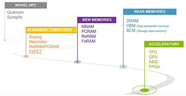
AI Era architectural changes are influencing both logic and memory. Machine learning algorithms make heavy use of matrix multiplication operations that are cumbersome in general-purpose logic, and this is driving a move to accelerators and their memories. AI compute includes two distinct memory tasks: first, storing the intermediate results of calculations; and second, storing the weights associated with trained models.

Performance and power are important in the cloud and in the edge, and innovations in memory can help. One approach using existing memory technologies is “near memories” whereby large amounts of working memory are condensed, placed in close physical proximity to logic, and connected via high-speed interfaces. As examples, 3D stacking and through-silicon vias are gaining traction. One major drawback of SRAM and DRAM as “working memories” in these applications is that they are volatile and need a constant supply of power to retain data—such as weights.

To reduce power in the cloud and edge, designers are evaluating new memories that combine high performance with non-volatility so that power is only needed during active read and write operations. Three of the leading new memory candidates are magnetic random-access memory (MRAM), phase-change RAM (PCRAM) and resistive RAM (ReRAM). 

Full article: Applied Materials Blog LINK
 
Additional read: Manufacturing Requirements of New Memories LINK

Tuesday, November 13, 2018

Spin Memory Teams With Applied Materials to Produce a Comprehensive Embedded MRAM Solution

FREMONT, Calif. — Spin Memory, Inc. (Spin Memory), the leading MRAM developer, today announced a commercial agreement with Applied Materials, Inc. (Applied) to create a comprehensive embedded MRAM solution. The solution brings together Applied’s industry-leading deposition and etch capabilities with Spin Memory’s MRAM process IP.


Key elements of the offering include Applied innovations in PVD and etch process technology, Spin Memory’s revolutionary Precessional Spin CurrentTM (PSCTM) structure (also known as the Spin Polarizer), and industry-leading perpendicular magnetic tunnel junction (pMTJ) technology from both companies. The solution is designed to allow customers to quickly bring up an embedded MRAM manufacturing module and start producing world-class MRAM-enabled products for both non-volatile (flash-like) and SRAM-replacement applications. Spin Memory intends to make the solution commercially available from 2019.

“In the AI and IoT era, the industry needs high-speed, area-efficient non-volatile memory like never before,” said Tom Sparkman, CEO at Spin Memory. “Through our collaboration with Applied Materials, we will bring the next generation of STT-MRAM to market and address this growing need for alternative memory solutions.”

“Our industry is driving a new wave of computing that will result in billions of sensors and a dramatic increase in data generation,” said Steve Ghanayem, senior vice president of New Markets and Alliances at Applied Materials. “As a result, we are seeing a renaissance in hardware innovation, from materials to systems, and we are excited to be teaming up with Spin Memory to help accelerate the availability of a new memory.”
About the PSC

Friday, October 26, 2018

$70m lab for next-generation semiconductors at National University of Singapore with Applied Materials

 Picosun ALD Tool in the NUS clean room
 
[NUS News LINK] NUS and Applied Materials — the world’s top semiconductor and display equipment company, and a leader in materials engineering solutions — have jointly established the Applied Materials-NUS Advanced Materials Corporate Lab, supported by the National Research Foundation (NRF). This $70 million collaboration, Applied Materials’ first university-based research laboratory, will focus on research and development (R&D) with the aim of developing and quickly commercialising innovative materials for manufacturing next-generation semiconductors.
From left: Vice President & Regional President (SEA) of Applied Materials Mr Brian Tan, Dr Raja, Mr Heng, NUS Chairman Mr Hsieh Fu Hua, NRF CEO Prof Low Teck Seng and Prof Tan officially launching the laboratory
Materials engineering has helped enable major advancements in semiconductor devices over the years, said Dr Prabu Raja, Senior Vice President at Applied Materials. “However, new applications in artificial intelligence require orders of magnitude improvements in chip performance and power efficiency. Materials innovation will have a critically important role in achieving these improvements,” he noted in his speech at the official launch of the laboratory on 25 October.


Monday, August 20, 2018

Overview of Applied Materials cobalt metallization for local interconnects

For those of you interested in the details behind the Applied Materials integrated cobalt metallization process Jonathan Bakke has written two informative blogs about it in Semiconductror Engineering:

(1) The Role Of Cobalt In Enabling AI - For continued performance, power, area and cost improvements, materials need to be engineered at the atomic scale.
(2) The Materials Side Of AI - What comes after tungsten fill for contacts and copper for the lowest-level interconnects?
The integrated cobalt solution using Applied Materials platforms (Applied Materials).

Jonathan Bakke is global product manager for Contact and Middle of Line Products in the Metal Deposition Products Business Unit at Applied Materials. He details the process flow and tool sets from Applied Materials involved in the complete BEOL Co metallization flow:

  • PVD titanium and ALD titanium nitride for the silicide and barrier layers
  • PVD cobalt serves as an anchor layer to ensure good cobalt adhesion to the bottom of the feature
  • CVD cobalt is then used to deposit a conformal film to bulk fill the feature
  • Anneal purifies and reflows the cobalt, removes the CVD seam, and merges crystal grains to form a more crystalline, lower resistance material
  • PVD cobalt for a thick overburden film
  • CMP removes overburden materials to create a smooth planar surface
  • E-beam technology monitors the process and detects voids

Wednesday, June 6, 2018

Applied Materials enables cobalt contact & interconnect for 7nm with pre-clean, PVD, ALD and CVD – on the Endura® platform

At IEDM 2017 in December both Intel and Globalfoundries presented cobalt encapsulation (liner and cap) for copper local interconnects as well as Co fill contacts for their 10nm resp 7nm technologies. Since then many have wondered about the unit process details behind the new cobalt integration and here we have it - The Applied Materials  complete cobalt solution as announced yesterday. Especially interesting that TiN ALD also is used as a cobalt seed/adhesio/dufusion barrier for cobalt contacts. The most interesting stuff you will finde here: LINK
[SANTA CLARA, Calif., June 05, 2018]  Applied Materials, Inc. today announced a breakthrough in materials engineering that accelerates chip performance in the big data and AI era.

In the past, classic Moore’s Law scaling of a small number of easy-to-integrate materials simultaneously improved chip performance, power and area/cost (PPAC). Today, materials such as tungsten and copper are no longer scalable beyond the 10nm foundry node because their electrical performance has reached physical limits for transistor contacts and local interconnects. This has created a major bottleneck in achieving the full performance potential of FinFET transistors. Cobalt removes this bottleneck but also requires a change in process system strategy. As the industry scales structures to extreme dimensions, the materials behave differently and must be systematically engineered at the atomic scale, often under vacuum. 
To enable the use of cobalt as a new conducting material in the transistor contact and interconnect, Applied has combined several materials engineering steps – pre-clean, PVD, ALD and CVD – on the Endura® platform. Moreover, Applied has defined an integrated cobalt suite that includes anneal on the Producer® platform, planarization on the Reflexion® LK Prime CMP platform and e-beam inspection on the PROVision™ platform. Customers can use this proven, Integrated Materials Solution to speed time-to-market and increase chip performance at the 7nm foundry node and beyond. 

“Five years ago, Applied anticipated an inflection in the transistor contact and interconnect, and we began developing an alternative materials solution that could take us beyond the 10nm node,” said Dr. Prabu Raja, senior vice president of Applied’s Semiconductor Products Group. “Applied brought together its experts in chemistry, physics, engineering and data science to explore the broad portfolio of Applied’s technologies and create a breakthrough Integrated Materials Solution for the industry. As we enter the big data and AI era, there will be more of these inflections, and we are excited to be having earlier and deeper collaborations with our customers to accelerate their roadmaps and enable devices we never dreamed possible.”

While challenging to integrate, cobalt brings significant benefits to chips and chip making: lower resistance and variability at small dimensions; improved gapfill at very fine dimensions; and improved reliability. Applied’s integrated cobalt suite is now shipping to foundry/logic customers worldwide.

Applied Materials, Inc. (Nasdaq:AMAT) is the leader in materials engineering solutions used to produce virtually every new chip and advanced display in the world. Our expertise in modifying materials at atomic levels and on an industrial scale enables customers to transform possibilities into reality. At Applied Materials, our innovations make possible the technology shaping the future. Learn more at www.appliedmaterials.com.