Showing posts with label ASD - Area Selective Deposition. Show all posts

Tuesday, April 2, 2019

RASIRC to Highlight Precise Water Vapor Delivery in Area Selective Deposition

CTO featured as industry expert on panel at upcoming ASD Workshop

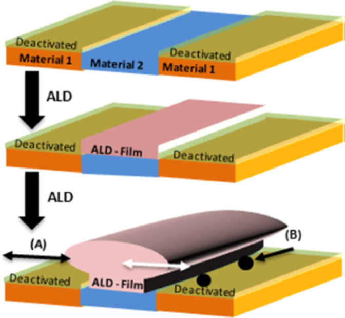
San Diego, Calif – March 29, 2019 – RASIRC will discuss test results for precise delivery of water vapor at the Area Selective Deposition (ASD) 2019 Workshop on April 4-5 in Leuven, Belgium. The company, a Silver Sponsor of the workshop, will review droplet and particle measurements as well as mass delivery under a variety of conditions. The RASIRC poster entitled “Precise Control of Water Vapor Delivery for ASD” will be displayed on Thursday April 4 and Friday April 5 as part of the workshop’s poster session. Additionally, RASIRC CTO Daniel Alvarez will be a speaking on the “Critical Challenges and Research Needs for ASD” panel during the 4th ASD workshop. The panel discussion will take place on Friday April 5 from 15:00 to 16:00.

“In order for the industry to take this to a high volume commercial level, we first must have an understanding of the underlying chemical pathways associated with ASD,” says Alvarez. “It is critical to control nucleation, which is best accomplished by the control of adsorption and surface properties on an atomic level.”
 
 
ASD Workshop is an annual event sponsored by ASM and IMEC. The workshop features leading academic and industry experts in surface chemistry, new processes, metrology, fields of applications and all technology needs and challenges for ASD.

“Controlled water addition at low concentration and temperature is vital to successful selectivity in ASD processes,” said Jeffrey Spiegelman, RASIRC President and Founder. “That is why we designed a water ampoule replacement that utilizes a membrane delivery system for precise delivery of droplet-free water vapor. Our data shows that we can achieve the required mass output in a repeatable and consistent manner.”

Spiegelman and Alvarez will be available to discuss the company’s ASD product line-up, which includes hydrogen peroxide and hydrazine gas delivery in addition to water vapor.

About RASIRC Products

RASIRC RHA enables the delivery of purified water vapor into low pressure processes. The membrane delivery system separates the liquid water and its headspace from directly seeing the process vacuum. The membrane assembly allows the mass transfer of water vapor at a known diffusion rate for a given set of parameters (temperature, pressure, surface area, carrier gas flow rate).

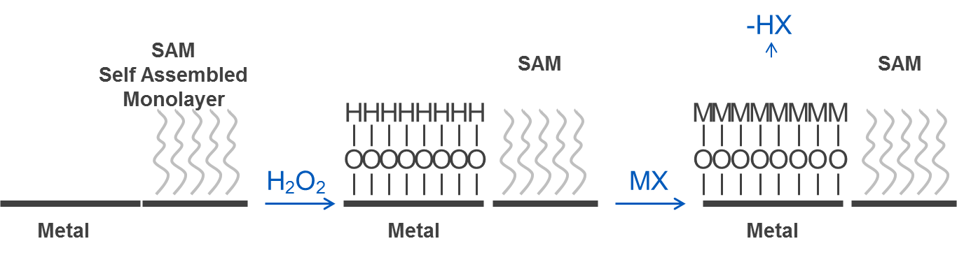
BRUTE® Peroxide is a novel oxidant that improves nucleation density at film interfaces when compared to other oxidants. Surface functionalization is more dense and initiation is faster using anhydrous hydrogen peroxide gas compared with alternatives. This can allow for better selectivity and less damage to metal surfaces in ASD processes.

BRUTE® Hydrazine enables uniform nitride deposition for Silicon and early transition metals at low temperature. BRUTE® Hydrazine may also be used as an atomic hydrogen source, where metals such as Ru, Cu, and Co may be cleaned and reduced. Hydrazine gas is generated in situ and is virtually water free. Brute Hydrazine has been formulated for a relatively high flash point for safer handling.

RASIRC Peroxidizer® provides high volumes of reactive H2O2/H2O mixtures for high throughput ALD. This reactive gas generator is ideal for roll-to-roll ALD coatings that require high speed deposition at reduced temperatures.

Additional RASIRC products include the RainMaker Humidification System (RHS) and the Hydrogen Peroxide Steamer (HPS). The RHS generates water vapor for oxidation applications and the HPS provides surface cleaning, preconditioning, wet thermal oxidation and residual carbon removal.

Monday, February 4, 2019

Extended deadline for ASD 2019 Workshop

We are pleased to announce that the deadline for ASD abstract submission has been extended until Sunday 10 February. This means you have an extra ten days to finalize your abstracts and submit them at: abstract@asd2019-workshop.org


The workshop will feature the following invited speakers:

Rudy J. Wojtecki (IBM, USA), Katie Nardi (LAM Research, USA), Kanda Tapily (TEL, USA), Chi-I Lang (AMAT, USA), John Tolle (ASM, USA), Han-Bo-Ram Lee (Incheon National University), Gregory Parsons (NC State University, USA), Matthias Minjauw (University of Gent, Belgium), Necmi Biyikli (University of Connecticut, USA), Mohamed Saib (IMEC, Belgium), Efrain A. Sanchez (IMEC, Belgium), John G. Ekerdt (University of Texas, USA).

The workshop will cover a wide range of topics, including the following:


Area selective epitaxy and area selective chemical vapor deposition: processes and mechanisms, defects control

Intrinsic selectivity of ALD processes: nucleation and interface studies, chemical selectivity in surface reactions, competitive adsorption, precursors design, modeling of surface reactions

Methods for area selective activation / deactivation: use of inhibitors (self-assembled monolayers, polymers), plasma-/beam-induced activation

Processes and mechanisms for area selective atomic layer deposition: deposition of metals or dielectrics, thermal/plasma enhanced ALD, 3D or patterned substrates, substrates preparation, sequential deposition/etching,

Metrology and defects control: surface characterization techniques, selective etching of defects

Applications of area selective deposition: semiconductor industry (integration needs of device makers, solutions proposed by the equipment makers), catalysis, energy generation and storage, etc.


On behalf of the organizing committee, it will be our pleasure to welcome you in Leuven.

Andrea Illiberi Program Chair of the 4th ASD workshop

Tuesday, January 15, 2019

CALL FOR PAPERS - 4th Area Selective Deposition (ASD) Workshop will be held on April 4th – 5th, 2019 in IMEC, Leuven (Belgium)


 Visit our website:

ASM and IMEC are proud to announce that the 4th Area Selective Deposition (ASD) Workshop will be held on April 4th – 5th, 2019 in IMEC, Leuven (Belgium).

This workshop will bring together leading experts from both academia and industry to share their vision and results on ASD. Based on a series of successful workshops at the: North Carolina State University in 2018, Eindhoven University of Technology in 2017 and IMEC in 2016, the two-days program will include invited and contributed speakers, a poster session and a reception on the evening of April 4th.

The workshop will cover a wide range of topics, including the following:

Area selective epitaxy and area selective chemical vapor deposition: processes and mechanisms, defects control

Intrinsic selectivity of ALD processes: nucleation and interface studies, chemical selectivity in surface reactions, competitive adsorption, precursors design, modeling of surface reactions

Methods for area selective activation / deactivation: use of inhibitors (self-assembled monolayers, polymers), plasma-/beam-induced activation

Processes and mechanisms for area selective atomic layer deposition: deposition of metals or dielectrics, thermal/plasma enhanced ALD, 3D or patterned substrates, substrates preparation, sequential deposition/etching,

Metrology and defects control:
surface characterization techniques, selective etching of defects

Applications of area selective deposition:
semiconductor industry (integration needs of device makers, solutions proposed by the equipment makers), catalysis, energy generation and storage, etc.

On behalf of the organizing committee, it will be our pleasure to welcome you in Leuven.

Andrea Illiberi

Program chair of the 4th ASD workshop

Friday, December 21, 2018

Area-selective ALD with high selectivity at TU Eindhoven

Here is a cool video for TU Eindhoven on Area-selective ALD with high selectivity just publishe in their AtomicLimits blog "Towards Area-Selective Atomic Layer Deposition with High Selectivity – Our perspective on area-selective ALD" by Adrie Mackus (LINK).


Monday, November 19, 2018

15 nm resolved patterns in Selective Area Atomic Layer Deposition

Here is an impressive and fundamental paper on selective area atomic layer deposition (SA-ALD)or just area selective deposition (ASD) that some prefer to call it.

The researchers at IBM has devleoped a bottom up approach on 300 mm pattern wafers that had been fabricated using standard trench first metal hardmask damascene scheme to create a line pattern of 36 nm pitch with single EUV exposures using low-k OMCTS 2.7 as the dielectric.
 
By deactivating ond surface with self-assembled monolayers (SAMs, Octadecylphosphonic acid) leaving another surface active for ALD processing (ZnO) they were able to produce 15 nm resolved patterns. One of the biggest challenges in the implementation of SA-ALD is the ability to maintain pattern fidelity and reduce defects during the ALD process (ZnO). 
 
Thank you Henrik Pedersen for sharing this paper!


Deactivating material is used to block one surface from ALD film growth. (A) ALD eventually leads to overgrowth of the film onto deactivated areas. (B) Defects in the deactivation layer can lead to the formation of locally deposited material. Published with permission from ACS Appl. Mater. Interfaces, 2018, 10 (44), pp 38630–38637 Copyright 2018 American Chemical Society.

Fifteen Nanometer Resolved Patterns in Selective Area Atomic Layer Deposition—Defectivity Reduction by Monolayer Design

Rudy Wojtecki, Magi Mettry, Noah F. Fine Nathel, Alexander Friz, Anuja De Silva, Noel Arellano, and Hosadurga Shobha
ACS Appl. Mater. Interfaces, 2018, 10 (44), pp 38630–38637
DOI: 10.1021/acsami.8b13896

Friday, November 16, 2018

4th Area Selective Deposition (ASD) workshop April 4th – 5th, 2019 in IMEC

[Announcment LINK] ASM and IMEC are proud to announce that the 4th Area Selective Deposition (ASD) Workshop will be held on April 4th – 5th, 2019 in IMEC, Leuven (Belgium).

News tip by Henrik Pedersen - Tack så mycket


This workshop will bring together leading experts from both academia and industry to share their vision and results about: fundamental aspects of surface chemistry, new processes, metrology, fields of applications, technology needs and integration challenges for ASD. Based on a series of successful workshops at the North Carolina State University in 2018, Eindhoven University of Technology in 2017 and at IMEC in 2016, the two-days program will include invited and contributed speakers, a poster session and a reception on the evening of April 4th.
 

Saturday, October 27, 2018

Area-selective ALD using Si precursors as inhibitors

Area-Selective Atomic Layer Deposition Using Si Precursors as Inhibitors

Rizwan Khan, Bonggeun Shong, Byeong Guk Ko, Jae Kwang Lee, Hyunsoo Lee, Jeong Young Park, Il-Kwon Oh, Shimeles Shumi Raya, Hyun Min Hong, Kwun-Bum Chung, Erik J. Luber, Yoon-Seok Kim, Chul-Ho Lee, Woo-Hee Kim, and Han-Bo-Ram Lee

Chem. Mater., Article ASAP
DOI: 10.1021/acs.chemmater.8b02774

Short-chain aminosilanes, namely, bis(N,N-dimethylamino)dimethylsilane (DMADMS) and (N,N-dimethylamino)trimethylsilane (DMATMS), have been used as Si precursors for atomic layer deposition (ALD) of SiO2. In this work, the DMADMS and DMATMS Si precursors are utilized as inhibitors for area-selective ALD (AS-ALD). The inhibitors selectively adsorb on a SiO2 surface but not on H–Si, so that SiO2 becomes selectively deactivated toward subsequent ALD. The deactivation of the SiO2 surface by the inhibitors was investigated using various experimental and theoretical methods, including surface potential measurements, spectroscopic ellipsometry, and X-ray photoelectron spectroscopy. Better inhibition was observed for ALD of Ru and Pt than for ALD of Al2O3 and HfO2. Through quantum mechanical and stochastic simulations, the difference in the blocking ability for noble metal and metal oxide ALD by the aminosilane inhibitors could be attributed to the inherently partial surface coverage by the inhibitors at their saturation and the reactivity of the subsequent ALD precursors. As silane inhibitors can be easily integrated with vacuum-based processes to facilitate high volume manufacturing of upcoming electronic devices, the current study provides a potential approach for the utilization of AS-ALD in pattern fabrication inside 3D nanostructures.


"Reprinted with permission from (DOI: 10.1021/acs.chemmater.8b02774). Copyright (2018) American Chemical Society."

Tuesday, September 18, 2018

IITC-MAM2019 First Call for Papers

The 22nd edition of the International Interconnect Technology Conference (IITC) is sponsored by the IEEE Electron Devices Society as the premier conference for interconnect technology. The 28th edition of the Materials for Advanced Metallization workshop (MAM) is devoted to research on materials properties and interactions of interconnect and silicide materials. These two conferences will be combined again in 2019 for the 3rd joint IITC-MAM conference and feature compelling invited talks and be proceeded by a materials workshop. 
 

Authors are encouraged to submit their original work describing innovative research and development in the critically important felid of on-chip interconnects. The conference seeks papers on all aspects of BEOL/MOL interconnects and metallization, including design, unit process, integration and reliability.

APPLICATION OF INTEREST

  • Advanced interconnects with low-k dielectrics
  • Beyond Cu interconnect, optical, wireless, and carbon
  • Contacts to MOS devices: Silicide, III-V, 2D materials
  • BEOL elements for Memory: 3D NAND, CBRAM, PCRAM, ReRAM, MRAM, DRAM
  • Advanced packaging and 3D/2.5D integration: WtW/CtW bonding, Interposer, TSV, CPI, Fan-Out techniques, Integrated Fan-Out
  • Smart technologies for interconnects: AI/neuromorphic, machine learning, big data.
TOPICS OF INTEREST
  • Process integration, advanced patterning for MOL/BEOL
  • Materials and Unit Processes: dielectrics, metals, barriers, wet, CMP, PVD, CVD, ALD, selective deposition/SAMs
  • Reliability and Failure analysis, techniques and methods
  • Advanced characterization: material analysis, analytical techniques, process modelling, defectivity, EPE
  • System scaling: design-technology co-optimization, embedded functionalities (memory, MEMS, Sensors...) Novel Systems/form factors: flexible, wearables, etc.
More information: LINK

Tuesday, June 12, 2018

Report from the 3rd Area Selective Deposition Workshop (ASD 2018) at North Carolina State University

In late April (April 29 – May 1, 2018) the 3rd Area Selective Deposition Workshop (ASD 2018), was held at North Carolina State University in Raleigh North Carolina USA (LINK). This years workshop was organized with full support from AVS and as for ALD and ALE Della Miller was in charge.

The Workshop brought together leading international scientists and engineers from academia and industry from all regions to share results and insights into: 1) fundamental principles and barriers to area selective deposition; 2) technological needs and challenges of ASD; 3) new chemical approaches and processes to address the expanding needs; and 4) surface characterization techniques and metrology innovation for ASD.

This third year the program was expanded to two days, including 11 invited presentations, an invited panel discussion, 18 contributed talks, and 15 posters and in between there was plenty of time for interaction over meals and social events.

ASD2018 brought together leading experts from 10 countries in Asia, Europe and America, to deliver and discuss more than 45 presentations. As the chart shows, this constitutes significant growth since the first ASD Workshop in 2016 (ASD2018 Book of Abstracts).

As a particular focus this year, the committee had chosen to highlight the challenge of selective deposition metrology, including an invited panel to discuss particular issues and techniques related to selectivity measurement and selective defect quantification.

It is clear that ASD is a fast growing field and may at some point in time reach the status as a stand alone segment with respect to processing, chemicals and equipment. Another indication can be seen that at the SPIE in February there was a high number of presentations and posters on combining ALD and ALE or just Area Selective Deposition.

Program Char Prof. Gregory N. Parsons of North Carolina State University, USA has asked to share some photos form the successful event (below). In addition, an article covering the event was just published by Chemical & Engineering News (LINK) including interviews and the latest insights from Dennis M. Hausmann (Lam Research), Gregory N. Parsons, Silvia Armini (invited speaker, imec), Dara Bobb-Semple and Stacey F. Bent (Stanford University), and Steven M. George (Colorado Boulder University).

Studying the Book of Abstract, my personal favorite is the atmospheric pressure micro-plasma printer for area-selective ALD presented by Prof. Kessels (TU Eindhoven). This technology is being commercialized by the Dutch company with InnoPhysics (LINK) and you can expect to hear more details about this exciting technology soon.

Rear view from the The StateView Hotel conference room (Photo: Gregory N. Parsons).
Junling Lu from University of Science and Technology of China, Hefei presenting "Bottom-up Engineering Catalyst Nanostructures using Area-Selective Atomic Layer Deposition" (Photo: Gregory N. Parsons).

Tuesday, May 22, 2018

Area selective ALD of hafnium nitride on Low-k by Veeco and Imec

Here is a recent Area Selective Deposition (ASD) paper by Veeco and Imec that got to be the Editor's Pick in JVSTA. ASD is important in scaling down semiconductor devices since it is a self aligned process meaning that you will not have an alignment issues with the previous patterning process when you continue to build your nano-electronic device layer by layer.
 
This paper is about growing hafnium nitride selectively by ALD on low-k dielectrics but not on copper. Hf3N4 is a decent high-k dielectric and can be transformed into HfSiON etc by annealing in oxygen atmosphere. Another option would be to let it act as a nucleation layer and barrier for e.g. a metal process by ALD, CVD or ELD. Here Imec and Veeco use vapor-deposited octadecanethiol as a masking layer on copper to enable area selective Hf3N4 atomic layer deposition on dielectrics studied by in-situ spectroscopic ellipsometry. 
 
This type of process could become an important tool in future bottom up fabricated process modules. As an example a process that is already in production is area selective CVD of Co on copper lines by using CoCOCp. Her Co metal only grows on the exposed copper lines and not on the low-k and thereby encapsulates the copper lines which reduces the risk for electromigration that leads to interconnect line fails.
 
Please check out the paper which is available as open sources : LINK


Tuesday, April 24, 2018

RASIRC to Present Anhydrous Hydrogen Peroxide Surface Preparation and Enhanced Nucleation for ASD at ASD2018

Area selective deposition is becoming increasingly important for the immense scaling effort continuously taking place in the semiconductor industry for Logic and Memory Devices. Today double and multiple pattering schemes using Plasma Enhanced ALD are in High Volume Manufacturing (HVM) for all sub 28 nm nodes and any moment now the industry expect to ramp EUV lithography, possibly at the 7 nm Foundry Node. Beyond that in a joint effort the researchers and the industry are looking for alternative patterning methods and many of them are based on so called bottom-up patterning.

To put things in perspective for ASD, one of the first area selective ALD processes in HVM was introduced in 300 mm DRAM manufacturing by Infineon Technologies in 2004 (90 nm Deep Trench DRAM presented in detail at IEDM 2004). This area selective ALD process relied on controlling the amount of hydroxyl groups in the upper part of a trench structure using the well-known TMA / H2O based process growing Al2O3. The goal was to let the process partially penetrate about 1 micron deep into very deep DRAM trenches to protect the silicon surface from a following isotropic etch that would widen the deep trench creating more surface and therefore allow a higher capacitance of the memory cell which is a key performance parameter in DRAM at about 25 fF/cell at that time.

In addition, the liner protected the collar region from dopant penetration keeping a well-defined dopant profile isolated from the wafer surface where the select transistor would later operate and it also defined a selective area for growth of Hemi-Spherical Grains (HSGs) another surface area expansion technology used in the DRAM industry. Please check the patent visualized below for many more details. This fascinating process was Self-Aligned and Area Selective in so many ways and kicked out a number of complex alternative integration paths saving a lot of $/wafer. By optimizing all process parameters it was possible to control the penetration depth of the liner, the transition region length down to the non-growth area, wafer uniformity and liner quality (density). This process was used until the end of the Deep Trench era which at this time had ~25% of the DRAM market but was killed at 65 nm when all companies had transitioned to stacked memory cells.

The Non-conformal ALD Al2O3 liner application as described in the US patent “Process for vertically patterning substrates in semiconductor process technology by means of inconformal deposition” (Figure from US7344953B2) 


Since then several things have happened. For one thing ALD has become a standard processing technology in Logic and Memory HVM forming its own Business Segment with an annual Equipment revenue >USD 1.5 Billion. Secondly, Atomic Layer Etching (ALE) has also entered HVM at the Logic 14 nm FinFET manufacturing. In parallel several efforts have begun to explore novel methods for ASD. These utilize Self-Assembled Monolayers, Patterned Photoresists, Selective CVD processes (e.g. Cobalt CVD), Plasma deposited films and other creative surface blocking agents and employing ALD and ALE in combination to trigger or block surface growth.  In parallel, reactive surfaces must be created for high nucleation and growth of metal oxide films.  An ideal surface treatment for the latter will:

                  Create high density surface functionalization
                  Have zero or minimal sub-surface oxidation
                  Lead to faster and more uniform nucleation versus H2O
                  Remain non-reactive with organic functionality or photoresist on adjacent surfaces

The use of the novel reactive chemistry, anhydrous hydrogen peroxide, has been largely ignored. This is due to: a lack of literature precedent; that H2O2 is typically delivered with H2O (multiple publications from K. Kukli et al at University of Helsinki and Tartu) where water dominates the reaction chemistry; and that only recently did this material become available by RASIRC (San Diego, USA) in an ampoule form that could be integrated into ASD process equipment.

Besides water, Ozone is an important co-reactant and oxidative precursor in ALD of metal oxides for, e.g., High-k dielectrics in DRAM Capacitors. Hydrogen Peroxide has similar oxidation properties to Ozone (oxidation potential O3 = 2.1V versus 1.8V for H2O2) while simultaneously having slightly stronger proton transfer properties than water (water pKa = 7.0 versus 6.5 for H2O2). According to Jeff Spiegelman (CEO and Founder of RASIRC) the key learning from early discoveries is the fact that H2O2 has a very weak O-O bond, where Bond Energy = 36 kcal/mole and you can imagine that it is thus much more readily available to conduct reactive surface chemistry in an ALD process than the oxygen atom in the water molecule.

RASIRC and their collaborative network of leading scientists and customers around the world have in recent years conducted exciting work with anhydrous hydrogen peroxide that demonstrates the following with regard to the required attributes for ASD:

                  Dry H2O2 creates 3-5 times higher nucleation surface density of hydroxyl groups
(-OH) versus water on metal surfaces
                  Monolayer hydroxyl (-OH) surface functionalization can be obtained by dry H2O2 on Si surfaces without sub-surface oxidation
                  Faster nucleation and growth of Al2O3  is observed utilizing dry H2O2 on Si-H surfaces versus H2O
Little to no Photoresist removal occurs from reaction with hydrogen peroxide at temperatures up to 300°C.

BRUTE Peroxide Ideal Chemistry for Area Selective Deposition yielding: High density surface hydroxylation, minimal sub-surface oxidation, faster and more uniform nucleation versus H2O, non-reactive with protecting groups on adjacent surfaces and Peroxide will grow a High Quality Metal Oxide
 

In addition, RASIRC has demonstrated that metal oxide films such as the most important ones; Aluminum oxide, Hafnium oxide, and Zirconium oxide have high quality film properties nearly identical to those grown by ozone methods.


In 3D-structures with extreme high aspect ratio (DRAM, 3DNAND) ozone will penetrate deep down the structure before reacting with the surface groups since the sticking coefficient is much smaller than H2O or preferably H2O2. This means that area selectivity employing ozone is difficult to achieve. You can imagine that Dry H2O2 would have been very beneficial back in 2004 for the non-conformal liner case described above by allowing use of a much thinner liner with higher density and therefore higher thru-put. Potentially also Dry H2O2 would allow for a sharper transition region – to be discovered!

RASIRC Chief Technology Officer Dan Alvarez will present additional details on the newly discovered reactivity of anhydrous hydrogen peroxide on several surfaces as well as outline some potential ASD pathways at AVS ASD2018, North Carolina State University, April 29 to May 1, 2018. (https://asd2018.avs.org/)

This is the 3rd time the ASD Workshop will be held. It is a fully supported AVS event and there has been a growing interest in ASD. In the future we can expect that it will form a solid business segment as ALD and ALE and bring in new players, both academic and industrial, in the exciting field of Atomic Level Processing!