Showing posts with label 3DNAND. Show all posts

Wednesday, June 15, 2016

The Future Paths for 3DNAND and ALD Opportunities

Here are brief summary of a recent interesting article in Semiconductor Engineering by Mark LaPedus on the topic of future paths for NAND Flash Memory, which is a big market for ALD with strong competition between ASM, Lam Research and others and high aspect ration Etch Technology from Applied Materials and Lam Research. I also and added some stuff that I found elsewhere.

What’s Next For NAND?

May 19th, 2016 - By: Mark LaPedus
http://semiengineering.com/whats-next-for-nand/

Scaling standard 2DNAND technology is coming to an end and all major NAND manufacturers are ramping 3DNAND today.  The NAND market leader (34%, see below) Samsung is in the lead a shipped their first 24 layer 128 gigabit chip in 2013 and have since then introduced a 32 layer are now since last year shipping the 3rd generation 48 layer chip offering a 256 gigabit storage capacity.

Intel and Micron has joined forces in NAND (joint 22% market share) and recently started shipping a 32 layer 3DNAND chip. The other duo, SanDisk (16%) and Toshiba (19%) as well as SK Hynix (10%) are trailing Samsung with their most current 48 layer chips.


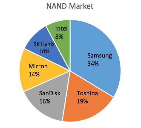
Current NAND Flash Market share - Source: Semiconductor Engineering.

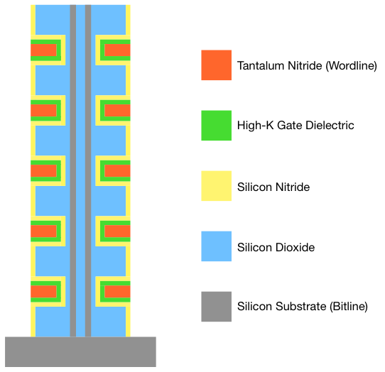
3DNAND Technology - Floating Gate vs. Charge Trap Flash

Floating Gate - Micron and Intel, currently uses the floating gate architecture


2015 Micron Presentation explaining the advantages with their 3D NAND floating gate technology shared with Intel.

Here you can read more about the Intel/Micron floating gate technology in an article by Dick James at Chipworks. I am not sure if ALD is used for the oxide and nitride layers but it is a possibility for sure due to high aspect ratio sttructures..


Charge Trap - Samsung, SK Hynix and the SanDisk/Toshiba are all steaming up the layers using charge trap NAND.


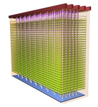
Samsung Promo video: Samsung's 3D V-NAND flash memory is fabricated using an innovative vertical design. Its vertical architecture stacks 32 cell layers on top of one another, rather than trying to decrease the cells' length and width to fit today's ever-shrinking form factors. [youtube.com]


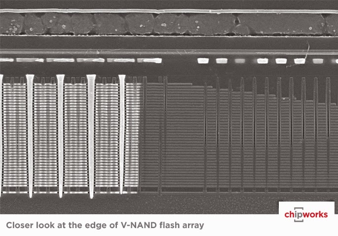
A Look Ahead at IEDM 2015, Solid State Technology, By Dick James, Senior Technology Analyst, Chipworks

Many available cross sections of available on the internet show high-k material (Al2O3) and a metal nitride (TiN) gate being used for the to connect to the tungsten control gate. I can only assess it as ALD being used in these extreme aspect ratios. 

According to a statement in the article made by Applied materials 3DNAND will make the step from 48 to 64 layers in 2016 and if it can be scaled further will be limited at some point by high aspect ration etch capability of 96 or 128 layers. However, I am a bit doubtful here that actually the technology will be limited by etch unit process engineers. As a comparison, many think that deep trench DRAM scaling was killed by high aspect ratio etch but it was not, it was rather the impossibility to scale the memory cell down from 8F2 , via 6F2 down ti a most compact 4F2 cell design. In any, case these are not extreme aspect ratios for ALD so either the etchers or the device physics will have to throw in the towel for 3DNAND momentarily. - to conclude there are two possible paths according to Mark LaPedus:

The first path:
"So going forward, NAND suppliers will simultaneously follow two parallel paths. The first path is to wait for the etch tools and other manufacturing techniques to arrive. And if they arrive on time, vendors could scale today’s 3D NAND device from 32- and 48-layers, to 64 layers, to 96 and then to 128."

The second path:
"The second path is to move towards string stacking technology. This involves stacking two or more individual devices on top each other. Each device is separated by an insulating layer. String stacking is already in the works. Recently, Micron presented a paper on a new 64-layer chip. Micron, according to multiple sources, stacked two 32-layer chips on top of each other. In theory, string stacking could involve several different combinations. For example, a vendor could stack three 32-layer chips, enabling a 96-layer device. In addition, a vendor could stack three 96-layer chips, resulting in a 288-layer product."

Saturday, December 5, 2015

Samsung is using an ALD Al2O3 gate dielectric for 3D V-NAND

Samsung seems to be using an ALD Al2O3 gate dielectric with a TiN/W Metal Gate according to Dick James at Chipworks who recently reported on the matter in front of IEDM 2015 (http://electroiq.com/chipworks_real_chips_blog/2015/12/02/a-look-ahead-at-iedm-2015/).

"Samsung started shipping their V-NAND last year, but that uses charge-trap storage, in which the electrons that make up the memory bits sit on a silicon nitride layer; the Intel/Micron device uses the conventional floating-gate method used in planar flash, where the electrons are stored on a polysilicon floating gate. It’ll be interesting to see the difference!"

Plan-view TEM images of Samsung V-NAND flash array (Chipworks) 

Looking at the rest of the stack one want to believe that also the TiN, SiO2 and SiN is deposited by ALD. However, knowing that those materials can successfully be deposited in a LPCVD or pulsed LPCVD process it can just as well be done in Large Batch furnaces from any of the companies ASM, Kokusai or Tokyo Electron. Those furnaces are for sure also capable of running the processes in a pure ALD mode though.

Below is a principal cross section of the first couple of cells in the Samsungs 3D NAND  from
Samsung SSD 850 Pro (128GB, 256GB & 1TB) Review: Enter the 3D Era by Kristian Vättö"


"NAND scaling in vertical dimension does not have the same limitations as scaling in the X and Y axes do. Because the cost of a semiconductor is still mostly determined by the die area and not by the height, there is no need to cram cells very close to each other. As a result, there is very little interference between the cells even in the vertical direction. Also, the usage of high-k dielectrics means that the control gate does not have to wrap around the charge trap. The result is that there is a hefty barrier of silicon dioxide (which is an insulator) between each cell, which is far more insulating than the rather thin ONO layer in 2D NAND."

Sunday, June 28, 2015

Micron’s 32-layer 3D NAND for production this year

The Tool makers of advanced semiconductor processing equipment look form inflection points for new advanced processing technology such as ALD. "The inflection points include the move towards multi-patterning. That’s an enormous driver of growth,” “It’s also the move to finFET from planar. It’s planar to 3D NAND, as well as the move to 3D packaging.” - Doug Bettinger, executive vice president and chief financial officer at Lam Research

Doug must be happy to hear that besides Samsung and Toshiba, Micron will move into pilot production of a 32-layer 3D NAND device in the second half of this year according to Electronics Weekly  The entry device will be a 32-layer device (pictured below) and it is believed that 3D NAND does not become cost-competitive with the most advanced planar NAND until it reaches 48 layers and Micron intends to introduce a 2nd generation 3D NAND which is, presumably, a 48-layer device, end of next year.

Micron 3DNAND 32 layer stack device

Sunday, May 17, 2015

2016 will be another growth year for OEM stocks and Atomic Layer Processing

2016 will be another growth year for OEM stocks and Atomic Layer Processing. In a report recently published by JP Morgan, analysts predicted another growth year in 2016 for Semiconductors stocks, driven by technology transitions in memory and 10nm FinFET. So this is good news for all Tier 1 OEMs with a number of ALD and ALE technologies in the game.

Technology transitions by memory companies :
  • continued 3D NAND ramps
  • additional 20nm conversions
  • initial 1Xnm DRAM deployments
Foundry and logic companies :
  • deploying FinFET technologies (especially 10nm FinFET) 
  • multi-patterning steps and vertical transistors
"In general, we see capital intensity increasing by 10-15% on a per wafer basis when transitioning from 14nm/16nm FinFET to 10nm FF and by 15+% when transitioning to 20nm and below DRAM / 3D NAND. The number of critical patterning layers is increasing dramatically – in the foundry/logic segment, the number of critical layers is increasing by over 3x going from 28 nm node to the 10nm node…a significant increase," the analysts added.
Read more: http://www.benzinga.com/analyst-ratings/analyst-color/15/05/5488523/jp-morgan-sees-another-growth-year-for-semiconductors-th#ixzz3aNRgk5q0

Below is an overview of some of the ALD and ALE technologies offered by the leading OEMs. It is ion sense complete yet so please let me know what is missing (jonas.sundqvist@baldengineering.com).

LAM Research


LAM Research reported in 2014 that "The latest in Lam's market-leading tungsten deposition product line, the ALTUS Max ICEFill system controls variability by providing void-free fill of the geometrically complex 3D NAND wordlines. Using a proprietary filling technique, the new system creates the tungsten wordlines with an inside-out atomic layer deposition (ALD) process. The ICEFill process completely fills the lateral (horizontal) lines without any voids, while at the same time minimizing deposition in the vertical channel area. As a result, both electrical performance and yield are enhanced."


Lam’s ALTUS systems combine CVD and ALD technologies to deposit the highly conformal films needed for advanced tungsten metallization applications (http://www.lamresearch.com/products/deposition-products).

Lam's new ALE capability on the 2300 Kiyo F Series conductor etch system provides both the productivity and technology needed. The product leverages fast gas switching and advanced plasma techniques in the reactor to boost throughput, while dynamic RF bias enables the directional etching required to remove material in high aspect ratio (deep and narrow) features. As the latest offering in Lam's market-leading Kiyo family, the 2300 Kiyo F Series system continues to provide superior uniformity and repeatability enabled by a symmetrical chamber design, advanced electrostatic chuck technology, and independent process tuning features.


  • Shallow trench isolation
  • Source/drain engineering
  • High-k/metal gate
  • FinFET and tri-gate
  • Double and quadruple patterning
  • 3D NAND

To learn how atomic layer deposition (ALD) and atomic layer etch (ALE) processes work, watch this video from LAM Research (www.youtube.com).

Applied Materials

CENTURA® ISPRINT™ TUNGSTEN ALD/CVD - The Applied Centura iSprint Tungsten ALD/CVD system provides complete contact/via fill for structures with aspect ratios ranging from 4:1 to 7:1 and extends the capability of tungsten technology to 20nm/16nm for logic and memory applications.


The iSprint system also delivers high throughput and low cost of consumables with an optimized ALD chamber design featuring a proprietary rapid gas delivery system and small chamber volume that enable fast, effective gas purging that uses less gas (www.appliedmaterials.com).

CENTURA® INTEGRATED GATE STACKThe system consists of an ALD HfO2 (hafnium oxide) deposition chamber and specialized chambers for interface layer oxide formation, post high-k nitridation, and post-nitridation anneal


The Centura Integrated Gate Stack system with ALD high-k chamber technology for 22nm and below uses Applied’s production-proven Centura Gate Stack platform to deliver the complete high-k process sequence in a controlled high vacuum environment without an “air break” (www.appliedmaterials.com).


Steven Hung, Ph.D. who specializes in integrating ALD into the transistor manufacturing process, dives deep into the chip to show what tomorrow's transistors look like, how they work, and how Applied can help the industry meet the challenges of fabricating these ultra-tiny structures to make faster, more power-efficient microchips 
(www.youtube.com).

Tokyo Electron

Tokyo electron has a number of ALD technologies and are very strong in batch processing that is used to large extent in DRAM production to get the cost per wafer down since DRAM is a commodity product.
  • TEL Formula - Mini batch, thermal processes including ALD for High-k, SiO2, SiN.
  • TEL INDY Plus - Large batch, thermal processes including ALD for High-k, SiO2, SiN.
  • TEL INDY IRad - Large batch, PEALD for ultra low temperature SiO2 and SiN.
  • TEL NT333 - Single wafer cluster tool for high t-put SiO2.

TEL INDY Large batch furnace for thermal processing and ALD (www.tel.com)


The NT333 applies inherent ALD concepts against conventional ALD processing to address the critical performance needs imposed by aggressive geometries. The NT333 can effectively deposit with a very tight thickness control, a range of less than 1A, while maintaining a productivity of 100+ wafers per hour. With a very unique reactor design, each of the ALD duty cycles enables the NT333 to deliver the high film quality which is typically compromised at low temperature regimes (<400C). (www.tel.com)

ASM International

ASM's ALD technologies, includes thermal ALD (Pulsar) for FinFET high-k metal gate stacks, and various applications of Plasma Enhanced ALD (Emerald) as an enabler for low temperature processing such as multiple patterning on resist and deposition of doped silicon oxide for solid state doping of FinFETs.


ASM’s Pulsar uses ALD to deposit the high-k dielectric materials required for advanced CMOS transistor gates ​and other applications. Pulsar is the benchmark ALD high-k tool for the industry. It was the first ALD system to be used for high-volume production at advanced customers for high-k metal gate transistors (www.asm.com).


EmerALD XP is a process module designed to deposit thin conformal metal and dielectric ​layers by atomic layer deposition (ALD) used for advanced CMOS gate stacks and other applications (www.asm.com).


​​​Eagle XP8 is a high productivity 300mm tool for PEALD applications. The Eagle XP8 PEALD system can be configured with up to four Dual Chamber Modules (DCM), enabling eight chambers in high volume production within a very compact footprint (www.asm.com).


ASM Chip Making Process (www.youtube.com)


Thursday, May 14, 2015

LAM Research MMP Technology Etch for Advanced Memory

"MMP technology enables atomic layer etching (ALE), providing extendibility and repeatability with atomic-scale fidelity"


Atomic-scale fidelity - Can you put it more beautiful?

LAM Research has developed a mixed-mode pulsing (MMP) technology that enables critical conductor etch for advanced memory like 3D NAND and DRAM. The technology is available for their Kiyo Product F Series chambers


LAM Research reports: The Kiyo F Series delivers high productivity while minimizing variability for advanced memory applications. Lam's MMP technology provides advanced profile and CD control for vertical profiles with good selectivity and tuning controls for consistent etch depths. These capabilities enable higher trim rate for 3D NAND staircase etch along with excellent repeatability, which is needed for manufacturing environments. Symmetric chamber design and radial tuning provide best-in-class uniformity, which is essential for minimizing CD variability. 

In addition, for new generations of advanced memory as well as logic devices, MMP technology enables atomic layer etching (ALE), providing extendibility and repeatability with atomic-scale fidelity.

By stacking memory cells vertically, NAND flash manufacturers can pack more storage capacity onto a smaller device, ease lithography requirements, and reduce manufacturing cost per bit. For multilayer 3D NAND structures, critical conductor etch processes include staircase etch and high aspect ratio (HAR) mask open for vertical channels. This mask open is crucial since it defines the CD and CD uniformity for subsequent etching of the vertical transistor channels. For staircase etch, equal-width "steps" are created at the edge of each dielectric-film pair throughout the 3D stack to form a staircase-shaped structure. Because of extensive repetition of these steps during device processing, etching at high throughput with stringent process control is vital. CD variability must be tightly managed since wordline contacts may otherwise miss landing on a step that is too narrow or uneven. 


Just for visualisation for the reader of this blog, here the advance HAR etch that is required and mastered by LAM MMP Technology described in a reverse engineering cross section by Chipworks from a SAMSUNG V-NAND Flash array (published here)

LAM Research further reports with respect to DRAM : For advanced DRAM devices, depth control is a key parameter, particularly for HAR front-end-of-line silicon etch applications. Concerns include aspect ratio loading, where etch rates vary because of differences in feature dimensions, and depth loading, where different etch depths may occur due to pattern density variations.

More detailed information on mixed-mode plasma pulsing (MMP) can be found in this patent by LAM Research:

Mixed mode pulsing etching in plasma processing systems US 20130168354 A1

Tuesday, July 8, 2014

Lam's New Products Deliver Critical Capability for Building 3D NAND Memory Devices

As reported today by Lam Research Corp. : Lam Research Corp. today unveiled its latest thin film deposition and plasma etch products for 3D NAND fabrication. As memory customers begin ramping production of these new devices, greater process control is needed for cost-effective manufacturing. Lam's new systems address this need for three of the most critical steps in forming 3D NAND memory cells: stack deposition (VECTOR® Q Strata(tm)), vertical channel etching (2300® Flex(tm) F Series), and tungsten wordline deposition (ALTUS® Max ICEFill(tm)).


The 3D NAND memory structures now moving to production involve numerous pairs of stacked films. Process variability on both the horizontal and vertical planes must be minimized for critical steps so that each memory cell in the final device delivers similar performance. Otherwise, variation in one step can be transferred and multiplied in subsequent steps, compounding errors and leading to poor device performance and low product yield. With 40 or more pairs of films in the stack, carefully managing even slight process fluctuations is essential. Lam's new products address these stringent control requirements.

As memory customers begin ramping production of these new devices, greater process control is needed for cost-effective manufacturing. Lam's new systems address this need for three of the most critical steps in forming 3D NAND memory cells: stack deposition (VECTOR® Q Strata™), vertical channel etching (2300® Flex™ F Series), and tungsten wordline deposition (ALTUS® Max ICEFill™).


The new VECTOR Q Strata PECVD (plasma enhanced chemical vapor deposition) system is used for depositing multilayer film stacks. For this critical 3D NAND process step, the system can perform both oxide/nitride (ONON) and oxide/polysilicon (OPOP) film stack deposition. To deposit the ultra-smooth, uniform films required to avoid compounding errors, the system's matched chambers deliver superior defectivity, film stress, and wafer bow performance. In addition, the VECTOR Q Strata also provides industry-leading productivity with the highest throughput per square meter of fab area available today. As the number of layers in these stacks continues to grow, high productivity is increasingly important for cost-effective production.

Once the stack of paired films is deposited, Lam's 2300 Flex F Series dielectric etch product is used to create a vertical channel through the stack. The new system can etch through high aspect ratio structures with minimal distortion or sidewall damage, while also tightly controlling etch profile uniformity across the wafer. This capability is critical since even small deviations can cause channel dimensions to differ from cell to cell, resulting in device performance variation. A proprietary high ion energy source with modulation of energies enables these results.

The latest in Lam's market-leading tungsten deposition product line, the ALTUS Max ICEFill system controls variability by providing void-free fill of the geometrically complex 3D NAND wordlines. Using a proprietary filling technique, the new system creates the tungsten wordlines with an inside-out atomic layer deposition (ALD) process. The ICEFill process completely fills the lateral (horizontal) lines without any voids, while at the same time minimizing deposition in the vertical channel area. As a result, both electrical performance and yield are enhanced.

"By focusing on collaboration at Lam Research, we are innovating faster and more effectively to deliver the enabling capabilities our customers need," said Rick Gottscho, executive vice president of Global Products. "With the support and expertise of our customers and research partners, Lam now offers three products -- VECTOR Q Strata, 2300 Flex F Series, and ALTUS Max ICEFill -- that are playing critical roles in the development and production ramp of 3D NAND memory devices."

Friday, May 16, 2014

ALE - Atomic Layer Etch emerges for 3D NAND, sub-20nm DRAMs and FinFETs

Atomic Layer Etch Finally Emerges - is a interesting blog post by Mark LaPedus (Executive Editor for manufacturing at Semiconductor Engineering) that you should really read if you want some insight into why we need ALE and why it has been difficult to develope this etch technique.
 
After nearly two decades of being confined to R&D labs, equipment makers are placing big bets on this next-gen plasma etch technology.
 
[...]
 
Lam’s Lill agrees that ALE will not replace RIE. “We will offer both technologies in one reactor,” Lill said. “We think they will be complementary for certain applications. But we are already seeing the transition (to ALE) in certain applications.”
 
ALE could be used for 3D NAND, sub-20nm DRAMs and finFETs, but there are still some challenges before ALE is running in the production fab. “There are still three grand challenges left,” Lill said. “One is that there are no secondary unintended reactions for ALE. For example, we don’t want extreme UV radiation in the reactor. Second, we want the unit steps to be discrete. And finally, we need self-limiting single unit steps. They are very difficult to find.”
 
Read more here and additional comments from experts from LAM Research, Applied Materials and Sematech : http://semiengineering.com/atomic-layer-etch-finally-emerges/ 

 
Illustration of the process steps in a plasma-enhanced ALE cycle for a silicon film etched by chlorine and argon. (Source Electroiq)
 
[please note that we used to know ALE as Atomic Layer Epitaxy until ALD - Atomic Layer Deposition took over]