Showing posts with label Graphene. Show all posts

Friday, March 13, 2015

Alabama Graphite Finds Natural Graphene in USA

Alabama Graphite is pleased to announce that it has found naturally occurring flake graphene at its Coosa Property in Alabama, USA. The graphene was obtained using an innovative and cost effective process, by Dr. Nitin Chopra of The University of Alabama under our sponsored research partnership.

Alabama Graphite Co
 
Graphite is made up of multiple layers of graphene stacked on top of each other. Graphene is a single layer of two dimensional (2-D) carbon atoms. Graphene is valued because it exhibits superior electrical, optical, mechanical and thermal properties. It is not only the strongest material known (200 times stronger than steel), but is also one of the most flexible.

“We believe that the discovery of naturally occurring single and multi-layer graphene, on the Coosa Property opens a completely new and unique business dimension for the Company,” stated Ron S. Roda, CEO of Alabama Graphite. “The biggest challenge today for commercial viability of graphene is cost. This presents a very exciting opportunity for our Company.”

“In my opinion, emerging technologies using graphene could greatly benefit from a cost effective processing methodology, with the potential for improved economics and increased production levels relative to any of the current methods used to create synthetic graphene,” commented Dr. Nitin Chopra. “The work done on the Company’s material has the potential to enhance the process of producing scalable, nano-manufactured graphene and graphene-based derivatives.”

Synthetic graphene is currently produced using a variety of expensive, tedious methods that do not lend themselves to large-scale production and are prone to produce defective graphene with uncontrolled flake size. Current synthetic methods for developing graphene include chemical vapor deposition (CVD), mechanical exfoliation, solution exfoliation, and chemo-mechanical methods. This implies higher costs including greater energy consumption, and extended manufacturing time.

The Company and Dr. Chopra continue to jointly develop methodologies to isolate graphene and graphene-based applications. Graphite flakes thinner than 100 nm are of significant interest because of their physical characteristics. Such thin graphite flakes ranging from one 2-D layer of carbon atoms (graphene) or multiple layers of 2-D carbon atoms stacked over each other (multi-layer graphene or graphite nanoplatelets) are of particular interest for developing advanced applications.

As shown in Figure 1 below, a moderately-sized (<5 μm, top right inset) single crystal flake of graphene, from the Coosa Property, is observed with a clearly visible carbon atom arrangement at high resolution (bottom right inset in Figure 1A). These flakes demonstrated very high quality Raman spectral features (G-band intensities, Figure 1B) with the ratio of disordered carbon signature to graphitic carbon signature of around ~0.15±0.05 (ID/IG). In addition, electron transparent flakes (bi-layer and multi-layer graphene) were observed in the analyzed samples.
 
Alabama Graphite, Corp. 
Figure 1A) High resolution TEM image of single-layer graphene. Inset (top right) shows low-resolution image of single-layer graphene. Inset (lower right) shows atomic scale TEM image indicating arrangement of carbon atoms (red hexagons) with bond length closely matching that of C-C in graphene network.
 
Figure 1B) Raman spectra for various graphene flakes showing significantly large G-band peak intensity as compared to D and 2D band. This also corresponds to very low ID/IG ratio of ~0.15 ± 0.05
 
Rick Keevil, P. Geo., a Director of the Company and VP of Project Development, is a Qualified Person as defined by National Instrument 43-101, has approved the disclosure of the scientific or technical information concerning the Coosa Property contained in this press release.  

Wednesday, March 11, 2015

Hybrid copper / graphene nanowires

As published by Phys.org - A new process for coating copper nanowires with graphene has been published by Purdue University - an ultrathin layer of carbon – lowers resistance and heating, suggesting potential applications in computer chips and flexible displays.

Until now it has been difficult to coat copper nanowires with graphene because the process requires chemical vapor deposition at temperatures of about 1,000 degrees Celsius, which degrades copper thin films and small-dimension wires. The researchers have developed a new process that can be performed at about 650 degrees Celsius, preserving the small wires intact, using a procedure called plasma-enhanced chemical vapor deposition (PECVD)

Read more at: http://phys.org/news/2015-03-hybrid-nanowires-eyed-flexible.html#jCp

Hybrid nanowires eyed for computers, flexible displays


This illustration depicts a copper nanowire coated with graphene - an ultrathin layer of carbon - which lowers resistance and heating, suggesting potential applications in computer chips and flexible displays. Credit: Purdue University graphic

Thursday, February 19, 2015

Processing of graphene on 300mm HKMG Si device wafers in a CMOS Fab at CNSE

Processing of graphene on 300mm Si wafers in a state-of-the-art CMOS fabrication facility is now possible thanks to research at College of Na- noscale Science and Engineering, SUNY Polytechnic Institute, Albany NY.

It has been demonstrated that working MOSFETs with graphene channels can be fabricated in a conventional 300mm CMOS fabrication line using state-of-the-art process tools. The building blocks shown  can be used to fabricate other novel device architectures that can take advantage of the unique properties of graphene or other interesting single-layer (i.e., 2D) materials. Further optimization of graphene transfer and contact schemes intended to reduce overall resistance are ongoing and will the focus of future research.

Graphene 4-C

Higher magnification view of 100nm contact. Dotted line shows expected location of graphene (Image Solid State Technology)

A gate-quality 4nm HfO2 dielectric was deposited using an ALD process. Graphene was then transferred onto this HfO2 surface. This approach eliminates the need for a gate-quality dielectric deposition over the graphene.

Tuesday, February 3, 2015

University of Manchester slim down LEDs using atom thick materials

Ultrathin, flexible and semi-transparent LEDs made from a mix of different atom thick materials have been created by researchers in the UK and Japan. Beyond their scientific importance, the researchers believe the design could have significant commercial potential. Other researchers agree, but says that a suitable method for producing the devices is still needed.
 

Since graphene's remarkable electrical properties were discovered, other monolayer materials followed whose electrical properties are often very different. While graphene is an excellent conductor, boron nitride is an insulator and some transition metal dichalcogenide (TMDCs) monolayers are semiconductors. Several research groups have developed simple van der Waals heterostructures, such as tunnelling transistors, by combining multiple layers. Now Konstantin Novoselov, who shared the 2010 physics Nobel prize with Andre Geim for their discovery of graphene, and colleagues at the University of Manchester, have produced LEDs using the most complex monolayer heterostructures ever created.
 

Light-emitting diodes by band-structure engineering in van der Waals heterostructures
F. Withers, O. Del Pozo-Zamudio, A. Mishchenko, A. P. Rooney, A. Gholinia, K. Watanabe, T. Taniguchi, S. J. Haigh, A. K. Geim, A. I. Tartakovskii & K. S. Novoselov
Nature Materials(2015) doi:10.1038/nmat4205 Published online 02 February 2015 

The advent of graphene and related 2D materials, has recently led to a new technology: heterostructures based on these atomically thin crystals. The paradigm proved itself extremely versatile and led to rapid demonstration of tunnelling diodes with negative differential resistance, tunnelling transistors, photovoltaic devices, and so on. Here, we take the complexity and functionality of such van der Waals heterostructures to the next level by introducing quantum wells (QWs) engineered with one atomic plane precision. We describe light-emitting diodes (LEDs) made by stacking metallic graphene, insulating hexagonal ​boron nitride and various semiconducting monolayers into complex but carefully designed sequences. Our first devices already exhibit an extrinsic quantum efficiency of nearly 10% and the emission can be tuned over a wide range of frequencies by appropriately choosing and combining 2D semiconductors (monolayers of transition metal dichalcogenides). By preparing the heterostructures on elastic and transparent substrates, we show that they can also provide the basis for flexible and semi-transparent electronics. The range of functionalities for the demonstrated heterostructures is expected to grow further on increasing the number of available 2D crystals and improving their electronic quality.

Heterostructure devices with a SQW and MQWs.

Saturday, September 13, 2014

Scientists Come up with ALD Technique to Repair Atom-sized Graphene Defects

As reported by The Korea Bizwire: Ulsan National Institute of Science and Technology said on September 10 that its College of Natural Sciences professor Kim Kwanpyo, jointly with Lee Han-Bo-Ram (Incheon National University), and Zhenan Bao and Stacey F. Bent (Stanford University), succeeded in developing a technique to repair graphene’s line defects by selectively depositing metal.

Graphene is pure carbon in the form of a very thin, nearly transparent sheet, one atom thick, with excellent mechanical, electrical properties. In order to apply graphene to photovoltaic cells, displays, or sensors, it must be made in large scale.

But graphene tended to crack and produce boundary lines, making it difficult to maintain excellent material properties. To address this problem, there have been attempts to deposit metal on graphene surface, which was not effective as the metal deposition was not selective enough to defective parts.

By using platinum, the research team successfully demonstrated the selective deposition of metal at chemical vapor deposited graphene’s line defects, notably grain boundaries, by atomic layer deposition. As a result, the team proved three times improved electrode and hydrogen gas sensors at room temperature. The research outcome was reported on the September 2 issue of Nature Communications (see abstract below).

Kim Kwanpyo, the principal author, said, “We used platinum in the latest experiment. But other metals such as gold and silver may be used in subsequent experiments to repair graphene defects and the applications may be expanded to other areas.”
 

Kwanpyo Kim, Han-Bo-Ram Lee, Richard W. Johnson, Jukka T. Tanskanen, Nan Liu, Myung-Gil Kim, Changhyun Pang, Chiyui Ahn, Stacey F. Bent, & Zhenan Bao
 
One-dimensional defects in graphene have a strong influence on its physical properties, such as electrical charge transport and mechanical strength. With enhanced chemical reactivity, such defects may also allow us to selectively functionalize the material and systematically tune the properties of graphene. Here we demonstrate the selective deposition of metal at chemical vapour deposited graphene’s line defects, notably grain boundaries, by atomic layer deposition. Atomic layer deposition allows us to deposit ​Pt predominantly on graphene’s grain boundaries, folds and cracks due to the enhanced chemical reactivity of these line defects, which is directly confirmed by transmission electron microscopy imaging. The selective functionalization of graphene defect sites, together with the nanowire morphology of deposited ​Pt, yields a superior platform for sensing applications. Using ​Pt–graphene hybrid structures, we demonstrate high-performance hydrogen gas sensors at room temperature and show its advantages over other evaporative ​Pt deposition methods, in which ​Pt decorates the graphene surface non-selectively.
 
 
Selective ​Pt growth by ALD on one-dimensional defect sites of polycrystalline CVD graphene.
 

Wednesday, September 3, 2014

UPDATE: Graphene depsoited by Xi'an Jiaotong University in a Picosun PEALD reactor

Graphene depsoited by Xi'an Jiaotong University in a Picosun ALD reactor.  A whole new method for the synthesis of graphene at low temperatures by means of remote plasma-enhanced atomic layer deposition (PEALD) is developed in this work and reported in the paper below.

Low-temperature remote plasma-enhanced atomic layer deposition of graphene and characterization of its atomic-level structure
Yijun Zhang,   Wei Ren,   Zhuangde Jiang,   Shuming Yang,   Weixuan Jing,   Peng Shi, Xiaoqing Wu and Zuo-Guang Ye 
J. Mater. Chem. C, 2014,2, 7570-7574
 

Graphene has attracted a great deal of research interest owing to its unique properties and many potential applications. Chemical vapor deposition has shown some potential for the growth of large-scale and uniform graphene films; however, a high temperature (over 800 °C) is usually required for such growth. A whole new method for the synthesis of graphene at low temperatures by means of remote plasma-enhanced atomic layer deposition is developed in this work. Liquid benzene was used as a carbon source. Large graphene sheets with excellent quality were prepared at a growth temperature as low as 400 °C. The atomic structure of the graphene was characterized by means of aberration-corrected transmission electron microscopy. Hexagonal carbon rings and carbon atoms were observed, indicating a highly crystalline structure of the graphene. These results point to a new technique for the growth of high-quality graphene for potential device applications.

UPDATE Press release from PICOSUN: Picosun Oy, the leading manufacturer of high quality Atomic Layer Deposition (ALD) equipment for global industries, reports the successful low temperature deposition of graphene, enabled by its PICOPLASMA™ remote plasma source system.
 
Only 400 oC deposition temperature, now demonstrated by an elite research group led by Prof. Wei Ren and Prof. Zuo-Guang Ye at Xi'an Jiaotong University, China, does not only widen the variety of graphene's applications but the employment of ALD, already a well-known and widely used method in the semiconductor industry markedly facilitates the material's penetration into modern micro- and nanoelectronics manufacturing.
 
"Groundbreaking results like the ones just obtained at Xi'an Jiaotong University naturally call for the latest, most cutting-edge technology and know-how on both ALD equipment manufacturing and process development. We at Picosun are proud that our four decades' cumulative experience in ALD system design has contributed to this significant leap forwards in graphene manufacturing, paving its way to real, tangible products in e.g. next generation consumer electronics, medical, ICT, and space applications," summarizes Juhana Kostamo, Managing Director of Picosun.
 
"We have used Picosun's Advanced PEALD (plasma-enhanced ALD) system to testify that atomic layer deposition is a viable new technique for the growth of high-quality graphene. More importantly, this work demonstrates the possibility of integration of graphene into semiconductor technologies for possible microelectronic device applications," states Prof. Wei Ren, director of the Electronic Materials Research Laboratory from Xi'an Jiaotong University, Xi'an, China.
 

Friday, May 23, 2014

MIT shows a new promising way to make sheets of graphene on wafers by CVD

MIT News reports - Now researchers at MIT and the University of Michigan have come up with a way of producing graphene, in a process that lends itself to scaling up, by making graphene directly on materials such as large sheets of glass. The process is described, in a paper published this week in the journal Scientific Reports, by a team of nine researchers led by A. John Hart of MIT. Lead authors of the paper are Dan McNerny, a former Michigan postdoc, and Viswanath Balakrishnan, a former MIT postdoc who is now at the Indian Institute of Technology.

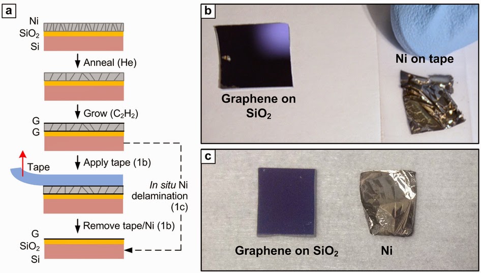
The new work, Hart says, still uses a metal film as the template — but instead of making graphene only on top of the metal film, it makes graphene on both the film’s top and bottom. The substrate in this case is silicon dioxide, a form of glass, with a film of nickel on top of it.
 
Using chemical vapor deposition (CVD) to deposit a graphene layer on top of the nickel film, Hart says, yields “not only graphene on top [of the nickel layer], but also on the bottom.” The nickel film can then be peeled away, leaving just the graphene on top of the nonmetallic substrate.
 
This way, there’s no need for a separate process to attach the graphene to the intended substrate — whether it’s a large plate of glass for a display screen, or a thin, flexible material that could be used as the basis for a lightweight, portable solar cell, for example. “You do the CVD on the substrate, and, using our method, the graphene stays behind on the substrate,” Hart says.
 
Read all details about this new approach to manufacture sheets of graphene in the open access Scientific Reports article below.
 
 
a) Process schematic, indicating Ni grain growth during annealing in He, followed by graphene growth under CVD conditions, and then removal of Ni using adhesive tape. Photos of substrates (~1 × 1 cm) and delaminated Ni films in case of b) ex situ tape delamination after graphene growth and c) in situ delamination during the graphene growth step. In the latter case the Ni film retains its integrity upon delamination and is moved to the side using tweezers after the sample is taken from the CVD system. (picture and caption from article below) 
Directfabrication of graphene on SiO2 enabled by thin film stress engineering
Daniel Q. McNerny, B. Viswanath, Davor Copic, Fabrice R. Laye, Christophor Prohoda, Anna C. Brieland-Shoultz, Erik S. Polsen, Nicholas T. Dee, Vijayen S. Veerasamy, A. John Hart   
Scientific Reports, Volume: 4, Article number: 5049, DOI:doi:10.1038/srep05049, Published

Abstract: We demonstrate direct production of graphene on SiO2 by CVD growth of graphene at the interface between a Ni film and the SiO2 substrate, followed by dry mechanical delamination of the Ni using adhesive tape. This result is enabled by understanding of the competition between stress evolution and microstructure development upon annealing of the Ni prior to the graphene growth step. When the Ni film remains adherent after graphene growth, the balance between residual stress and adhesion governs the ability to mechanically remove the Ni after the CVD process. In this study the graphene on SiO2 comprises micron-scale domains, ranging from monolayer to multilayer. The graphene has >90% coverage across centimeter-scale dimensions, limited by the size of our CVD chamber. Further engineering of the Ni film microstructure and stress state could enable manufacturing of highly uniform interfacial graphene followed by clean mechanical delamination over practically indefinite dimensions. Moreover, our findings suggest that preferential adhesion can enable production of 2-D materials directly on application-relevant substrates. This is attractive compared to transfer methods, which can cause mechanical damage and leave residues behind.      

Wednesday, May 21, 2014

Hybrid technology for 2D electronics by graphene/molybdenum disulfide heterostructures grown by CVD

Nanotechweb.org reports that Researchers in the US have unveiled a new CMOS-compatible technology to integrate different two-dimensional materials into a single electronic device. The team, led by Tomás Palacios of the Massachusetts Institute of Technology, constructed large-scale electronic circuits based on graphene and molybdenum sulphide heterostructures grown by chemical vapour deposition where MoS2 was used as a transistor channel, and graphene as contact electrodes and circuit interconnects. The fabrication process itself might be extended to fabricate heterostructures from any type of 2D layered material with potential applications in flexible and transparent electronics, sensors, tunnelling FETs and high-electron mobility transistors.
 
Demonstration of a novel technology for constructing large-scale electronic systems based on graphene/molybdenum disulfide (MoS2) heterostructures grown by chemical vapor deposition.
 
Mor details on this work in the article below:
 
Lili Yu, Yi-Hsien Lee, Xi Ling, Elton J. G. Santos, Yong Cheol Shin , Yuxuan Lin, Madan Dubey, Efthimios Kaxiras, Jing Kong, Han Wang, and Tomás Palacios
Nano Lett., DOI: 10.1021/nl404795z Publication Date (Web): May 8, 2014

Abstract: Two-dimensional (2D) materials have generated great interest in the past few years as a new toolbox for electronics. This family of materials includes, among others, metallic graphene, semiconducting transition metal dichalcogenides (such as MoS2), and insulating boron nitride. These materials and their heterostructures offer excellent mechanical flexibility, optical transparency, and favorable transport properties for realizing electronic, sensing, and optical systems on arbitrary surfaces. In this paper, we demonstrate a novel technology for constructing large-scale electronic systems based on graphene/molybdenum disulfide (MoS2) heterostructures grown by chemical vapor deposition. We have fabricated high-performance devices and circuits based on this heterostructure, where MoS2 is used as the transistor channel and graphene as contact electrodes and circuit interconnects. We provide a systematic comparison of the graphene/MoS2 heterojunction contact to more traditional MoS2-metal junctions, as well as a theoretical investigation, using density functional theory, of the origin of the Schottky barrier height. The tunability of the graphene work function with electrostatic doping significantly improves the ohmic contact to MoS2. These high-performance large-scale devices and circuits based on this 2D heterostructure pave the way for practical flexible transparent electronics.

Monday, May 19, 2014

Improved supercapacitors using ruthenium oxide RGM foam by University of California

As reported today by Sean Nealon, UC Riverside, Researchers at the Univ. of California, Riverside have developed a novel nanometer scale ruthenium oxide anchored nanocarbon graphene foam architecture that improves the performance of supercapacitors, a development that could mean faster acceleration in electric vehicles and longer battery life in portable electronics.

Read the full story here in the R&D Mag or check out the original OPEN ACCESS publication bellow:
 
Hydrous Ruthenium Oxide Nanoparticles Anchored to Graphene and Carbon Nanotube Hybrid Foam for Supercapacitors
Wei Wang, Shirui Guo, Ilkeun Lee, Kazi Ahmed, Jiebin Zhong, Zachary Favors, Francisco Zaera, Mihrimah Ozkan & Cengiz S. Ozkan          
Scientific Reports 4, Article number: 4452 doi:10.1038/srep04452, 25 March 2014

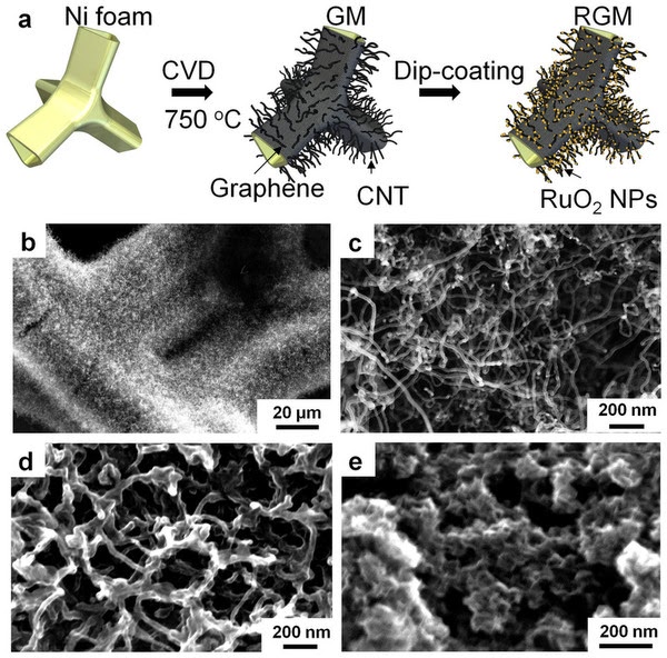
Abstract: In real life applications, supercapacitors (SCs) often can only be used as part of a hybrid system together with other high energy storage devices due to their relatively lower energy density in comparison to other types of energy storage devices such as batteries and fuel cells. Increasing the energy density of SCs will have a huge impact on the development of future energy storage devices by broadening the area of application for SCs. Here, we report a simple and scalable way of preparing a three-dimensional (3D) sub-5 nm hydrous ruthenium oxide (RuO2) anchored graphene and CNT hybrid foam (RGM) architecture for high-performance supercapacitor electrodes. This RGM architecture demonstrates a novel graphene foam conformally covered with hybrid networks of RuO2 nanoparticles and anchored CNTs. SCs based on RGM show superior gravimetric and per-area capacitive performance (specific capacitance: 502.78 F g−1, areal capacitance: 1.11 F cm−2) which leads to an exceptionally high energy density of 39.28 Wh kg−1 and power density of 128.01 kW kg−1. The electrochemical stability, excellent capacitive performance, and the ease of preparation suggest this RGM system is promising for future energy storage applications.

(a) Schematic illustration of the preparation process of RGM nanostructure foam. SEM images of (b–c) as-grown GM foam (d) Lightly loaded RGM, and (e) heavily loaded RGM. (Source : article above)


Check out the performance in this Ragone plot - Woah - pretty high energy density material!


(a) EIS plots and (b) high frequency region EIS plots of GM, RGM, a control sample (RuO2 nanoparticles only), respectively. (c) Ragone plot related to energy densities and power densities of the packaged whole cell RGM SC, GM SC, RuO2 nanoparticles SC, hydrous ruthenium oxide (RuO2)/graphene sheets composite (GOGSC), RuO2 nanowire/single walled carbon nanotube (SWNT) hybrid film. (Source: articlew above)


Friday, April 25, 2014

Paper-based ultracapacitors with carbon nanotubes-graphene composites

As reported by EE Times: Ultracapacitors, also called supercapacitors, serve as temporary energy storage that can quickly charge and discharge for everything from regenerative brakes in electric vehicles to cordless power tools that recharge in 90 seconds to stabilizing computer power supplies. Now researchers at George Washington University's Micro-Propulsion and Nanotechnology Laboratory report that superior ultracapacitors can be constructed from an inexpensive hybrid composite of graphene flakes mixed with single-walled carbon nanotubes.
 
Full report can be found in the JAP paper below


Prototype of an ultracapacitor device based on carbon nanostructures.

Paper-based ultracapacitors with carbon nanotubes-graphene composites
Jian Li, Xiaoqian Cheng, Jianwei Sun, Cameron Brand, Alexey Shashurin, Mark Reeves and
Michael Keidar
J. Appl. Phys. 115, 164301 (2014); http://dx.doi.org/10.1063/1.4871290

In this paper, a paper-based ultracapacitors were fabricated by the rod-rolling method with the ink of carbon nanomaterials, which were synthesized by arc discharge under various magnetic conditions. Composites of carbon nanostructures, including high-purity single-walled carbon nanotubes (SWCNTs) and graphene flakes were synthesized simultaneously in a magnetically enhanced arc. These two nanostructures have promising electrical properties and synergistic effects in the application of ultracapacitors. Scanning electron microscope, transmission electron microscope, and Raman spectroscopy were employed to characterize the properties of carbon nanostructures and their thin films. The sheet resistance of the SWCNT and composite thin films was also evaluated by four-point probe from room temperature to the cryogenic temperature as low as 90 K. In addition, measurements of cyclic voltammetery and galvanostatic charging/discharging showed the ultracapacitor based on composites possessed a superior specific capacitance of up to 100 F/g, which is around three times higher than the ultracapacitor entirely fabricated with SWCNT.

Tuesday, April 22, 2014

Trinity College Dublin showcase production of graphene by shear mixing

To progress from the laboratory to commercial applications, it will be necessary to develop industrially scalable methods to produce large quantities of defect-free graphene. Trinity College Dublin Ireland show that high-shear mixing of graphite in suitable stabilizing liquids results in large-scale exfoliation to give dispersions of graphene nanosheets.

Or as The Daily Mail puts it "How to make a supermaterial in the sink: Scientists find washing up liquid and a blender can be used to make graphene"
Scalable production of large quantities of defect-free few-layer graphene by shear exfoliation in liquids

Keith R. Paton, Eswaraiah Varrla, Claudia Backes, Ronan J. Smith, Umar Khan, Arlene O’Neill, Conor Boland, Mustafa Lotya, Oana M. Istrate, Paul King, Tom Higgins, Sebastian Barwich, Peter May, Pawel Puczkarski, Iftikhar Ahmed, Matthias Moebius, Henrik Pettersson, Edmund Long, João Coelho, Sean E. O’Brien, Eva K. McGuire, Beatriz Mendoza Sanchez, Georg S. Duesberg, Niall McEvoy, Timothy J. Pennycook, Clive Downing, Alison Crossley, Valeria Nicolosi & Jonathan N. Coleman
 
Nature Materials DOI: doi:10.1038/nmat3944 Published online:
 
To progress from the laboratory to commercial applications, it will be necessary to develop industrially scalable methods to produce large quantities of defect-free graphene. Here we show that high-shear mixing of graphite in suitable stabilizing liquids results in large-scale exfoliation to give dispersions of graphene nanosheets. X-ray photoelectron spectroscopy and Raman spectroscopy show the exfoliated flakes to be unoxidized and free of basal-plane defects. We have developed a simple model that shows exfoliation to occur once the local shear rate exceeds 104 s−1. By fully characterizing the scaling behaviour of the graphene production rate, we show that exfoliation can be achieved in liquid volumes from hundreds of millilitres up to hundreds of litres and beyond. The graphene produced by this method performs well in applications from composites to conductive coatings. This method can be applied to exfoliate BN, MoS2 and a range of other layered crystals.
 
 
Production of graphene by shear mixing (graphical abstract Nature Materials)
 

Monday, April 21, 2014

LG and researchers at ETH Zürich announce graphene membrane breakthrough

As reported by Solid State Technology : "Researchers from LG Electronics (LG) and Swiss university ETH Zurich (Swiss Federal Institute of Technology Zurich) have developed a method to greatly increase the speed and efficient transmission of gas, liquid and water vapor through perforated graphene, a material that has seen an explosion of scientific interest in recent years. The findings open up the possibility in the future to develop highly efficient filters to treat air and water. [...]  developed a reliable method for creating 2D membranes using chemical vapor deposition (CVD) optimized to grow graphene with minimal defects and cracks to form graphene layers thinner than 1nm (nanometer). Using a focused ion beam (FIB), the researchers then drilled nanopores in double layers of graphene to produce porous membranes with aperture diameters between less than 10nm and 1µm (micrometer). Testing various sized perforations, the researchers found that their graphene membrane resulted in water permeance five- to sevenfold faster than conventional filtration membranes and transmission of water vapor several hundred times higher compared to today’s most advanced breathable textiles such as Gore-Tex."
 
 
The full report by Kemal Celebi et al can be read in Science publication below:
 

Kemal Celebi, Jakob Buchheim, Roman M. Wyss, Amirhossein Droudian, Patrick Gasser, Ivan Shorubalko, Jeong-Il Kye, Changho Lee, Hyung Gyu Park

Science 18 April 2014: Vol. 344 no. 6181 pp. 289-292,  DOI: 10.1126/science.1249097                        
A two-dimensional (2D) porous layer can make an ideal membrane for separation of chemical mixtures because its infinitesimal thickness promises ultimate permeation. Graphene—with great mechanical strength, chemical stability, and inherent impermeability—offers a unique 2D system with which to realize this membrane and study the mass transport, if perforated precisely. We report highly efficient mass transfer across physically perforated double-layer graphene, having up to a few million pores with narrowly distributed diameters between less than 10 nanometers and 1 micrometer. The measured transport rates are in agreement with predictions of 2D transport theories. Attributed to its atomic thicknesses, these porous graphene membranes show permeances of gas, liquid, and water vapor far in excess of those shown by finite-thickness membranes, highlighting the ultimate permeation these 2D membranes can provide.

Friday, April 4, 2014

Samsung breakthru in wafer-scale growth of graphene

Samsung Advanced Institute of Technology and Sungkyunkwan University, publish results on wafer-scale growth of single-crystal monolayer graphene in Science. 
 
 
Published Online April 3 2014, Science DOI: 10.1126/science.1252268

The uniform growth of single-crystal graphene over wafer-scale areas remains a challenge in the commercial-level manufacturability of various electronic, photonic, mechanical, and other devices based on graphene. Here, we describe wafer-scale growth of wrinkle-free single-crystal monolayer graphene on silicon wafer using a hydrogen-terminated germanium buffer layer. The anisotropic twofold symmetry of the germanium (110) surface allowed unidirectional alignment of multiple seeds, which were merged to uniform single-crystal graphene with predefined orientation. Furthermore, the weak interaction between graphene and underlying hydrogen-terminated germanium surface enabled the facile etch-free dry transfer of graphene and the recycling of the germanium substrate for continual graphene growth.

More on this story at Extrem Tech: http://www.extremetech.com/extreme/179874-samsungs-graphene-breakthrough-could-finally-put-the-wonder-material-into-real-world-devices

Friday, March 28, 2014

SIMIT in Shanghai reports HfO2 growth directly on graphene by ALD

According to a fresh publication HfO2 can be grown directly on Graphene using a H2O/TEMAHf ALD process. Nanowerk.com reports from the team led by Xinhong Cheng at the Shanghai Institute of Microsystem and Information Technology (part of the Chinese Academy of Sciences), turned to a compound with a very unusual name: Tetrakis(ethylmethylamino)hafnium, or TEMAH. At 80 degrees Celsius (176 degrees Fahrenheit), TEMAH is a gas from which hafnium oxide (HfO2), a proven high-k dielectric can be derived. Unfortunately, getting the HfO2 to stick to graphene wasn't easy. "Using a traditional ALD techniques, we blew TEMAH into the deposition chamber with the hope that the HfO2 produced would be absorbed by the graphene substrate; but it would not stick," says Li Zheng, lead author on the JVSTA paper. "So, we pre-treated the substrate with water because we knew it would be absorbed onto the graphene and likely act as a nucleation [growth initiation] site. And that's what we found. TEMAH is attracted to the absorbed water, allowing a HfO2 layer to grow directly - and tightly - on the graphene surface."


Read more: Need your dielectric to stick to graphene? Just add water http://www.nanowerk.com/nanotechnology_news/newsid=34990.php#ixzz2xILrE6lH
Here is the abstract and link to the paper in JVSTA:

HfO2 dielectric film growth directly on graphene by H2O-based atomic layer deposition


J. Vac. Sci. Technol. A 32, 01A103 (2014); http://dx.doi.org/10.1116/1.4828361

"Due to its exceptionally high carrier mobility, International Technology Roadmap for Semiconductors considers graphene to be among the candidate materials for postsilicon electronics. In order to realize graphene-based devices, thin and uniform-coverage high-κ dielectrics without any pinholes on top of graphene is required. There are no dangling bonds on defect-free graphene surface; it is difficult to grow uniform-coverage high-κ dielectrics on graphene directly by atom layer deposition. Meanwhile, degradation of defects in graphene/high-κ structure is necessary for the optimization of high-κ dielectrics fabrication technology. Here the authors report on a H2O-based atom layer deposition method used for HfO2 growth, where physically adsorbed H2O molecules on graphene surface act as oxidant, and self-limit react with metal precursors to form HfO2 film onto graphene directly. Raman spectra reveal H2O-based atom layer deposition method will not introduce defects into graphene. The surface root mean square of HfO2 films is down to 0.9 nm and the capacitance of HfO2 films on graphene is up to 2.7 μF/cm2, which indicate high quality and compactness of HfO2 films. "