Showing posts with label precursors. Show all posts

Saturday, March 5, 2022

Electronic Gas Markets – Strong Growth, Pressing Supply-Chain Issues

San Diego, CA, March 3, 2022: TECHCET—the electronic materials advisory firm — announced a positive growth outlook for Electronic Gases through 2026. The 2022 Electronic Gas market is expected to top US$7 billion, driven mainly by logic chip fab expansions. Despite an expected 8% CAGR, there are pressing supply-chain issues, both nearer term and possibly longer term, exist in this industry segment. The Russia-Ukraine war is sparking growing concerns relating to the availability of gases such as neon, helium and other gases critical to semiconductor production around the globe.


The turmoil in the region, and related economic sanctions against Russia, will likely affect several key gases used by the semiconductor industry. Neon and helium are two examples. TECHCET’s latest analysis shows that majority of all high purity neon imports into the US is coming from the Ukraine. This represents <50% of total US demand.

TECHCET’s contacts in Ukraine indicate that rare gas purifiers in Ukraine have been temporarily shut down due to the conflict. So far there has only been an interruption of 5-6 days. However, if the fighting lingers on this could have a major impact on the chip industry that has been pushing hard to increase production.

Many of the supply-chains that support the industry are running thin on capacity. Investments in more material production has been lacking and demand for materials has been growing so fast that material pinch points exist in nearly every material segment, including gas processing equipment and subsystems. On-going issues on lead-times for all types of components related to gas processing (tool gas box upgrades, precursor deliver systems, bulk refill) are expected to impact lead-times for gas and precursor supply systems

“Even those material supply-chains that were looking fairly balanced in 2020 are increasingly getting pinched and any perturbation in the supply-chain can cause shortage issues,” said Lita Shon-Roy, TECHCET’s President & CEO. Helium is a prime example where hiccups in the supply-chain are causing increased lead-times and availability problem as the chip industry pushes up their demand. The US BLM, the US’s key source of helium, has been experiencing maintenance issues, delaying product availability, and Russia’s Gazprom purified helium production has been delayed (6 months or more) due to fire incidents over the past several months. “Add war into the mix and supply can be even further strained,” offered Shon-Roy.

As new semiconductor device fabs come online in the next few years, supply constraints may appear for other gases (B2H6, WF6, NF3, CF-gases) as demand increases are expected to outpace supply.

For more details on the Electronics Gas market segments and growth trajectory go to:

Don’t forget to register for the 2022 Critical Materials Conference (CMC) on April 28-29 in Chandler, AZ.

Thursday, February 17, 2022

RASIRC Provide Record Low Resistivity Titanium Nitride Film Fabricated by Thermal ALD

Ultra-dry hydrazine enables growth at low temperature

San Diego, Calif – January 18, 2022 – An IITC paper authored by researchers from UCSD, Samsung, and RASIRC demonstrated record low resistivities for low temperature titanium nitride (TiN) films grown by thermal ALD process. Films yielded resistivities below 200 µohm-cm. The process used titanium tetrachloride (TiCl4) and ultra-dry anhydrous hydrazine along with surface treatments to further reduce surface impurities. The reduction of moisture was key. This reduction was achieved by a high vacuum ALD process combined with anhydrous hydrazine with moisture below 100ppb.

Low resistivity is an indicator of a high-quality film that works well as a barrier layer or conductor. TiN thin films are used as diffusion barriers for cobalt (Co) and tungsten (W) metal layers as well as gate metal in CMOS devices due to their high electrical conductivity and related low resistivity.

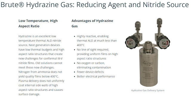
Historically, TiN films have been fabricated with ammonia and plasma. However, new three-dimensional designs with high aspect ratios (HAR) impose severe process limitations on plasma efficacy due to line-of-sight issues. Thermal ALD processes have a non-directional advantage over plasma if the process chemistry is reactive enough.

By replacing ammonia with hydrazine, reactivity is increased in the ALD process. This enables processing at lower temperatures needed for backend processes. Low temperature ALD is needed to avoid degradation of previously deposited structures. These breakthroughs make it possible for new 3D architectures like nanoribbons and nanotubes to move into high volume manufacturing.

“Once a low water background can be achieved in the tool, it is critical that the hydrazine precursor be as dry as possible to prevent oxygen incorporation in the film,” said RASIRC Founder and CEO Jeffrey Spiegelman. “Through proper tool design and ultra-dry BRUTE® Hydrazine, high quality titanium nitride films can be grown, as shown in the research.”

Details on the research were published in IEEE Xplore following the 2021 IEEE International Interconnect Technology Conference (IITC). For more information, contact RASIRC.


BRUTE Hydrazine

BRUTE Hydrazine enables uniform nitride deposition for titanium and early transition metals at low temperature. BRUTE Hydrazine may also be used as an atomic hydrogen source, where metals such as Ru, Cu, and Co may be cleaned and reduced. Brute Hydrazine has been formulated with a higher flash point for safer handling.

About RASIRC

RASIRC transforms liquids into dynamic gases that power process innovation in semiconductor and adjacent markets. By commercializing molecules for lower temperature processes, RASIRC patented technology enables the manufacture of atomic-scale oxides, nitrides, and metals. Innovative products such as BRUTE Peroxide, Brute Hydrazine, the Peroxidizer®, and Rainmaker® Humidification Systems are being used to develop solutions for 5G, AI, IOT, and advanced automation.


What makes RASIRC a unique industry leader is our technical expertise and commitment to solving complex industry challenges for our customers. Our team of industry experts has a proven track record of being first to market by efficiently delivering state of the art technology that reduces cost, improves quality, and dramatically improves safety. With our customers at the forefront of all we do, we continue to research, develop, and design innovative products that purify and deliver ultra-pure gas from liquids for the semiconductor and related markets. Contact RASIRC to help solve your complex problems.


P: 858-259-1220, email info@rasirc.om or visit http://www.rasirc.com


Thursday, January 27, 2022

ALD InGaN with single precursor pulse of In & Ga

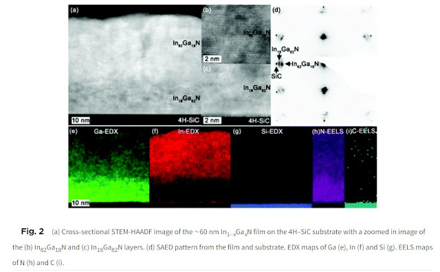
Polla Rouf of Pedersen Group in Linköping Sweden, just published an ALD approach to metastable In1−xGaxN with 0.1 < x < 0.5 based on solid In- and Ga-precursors that were co-sublimed into the deposition chamber in one pulse. A near In0.5Ga0.5N film with a bandgap value of 1.94 eV was achieved on a Si(100) substrate. Epitaxial In1−xGaxN(0002) was successfully grown directly on the 4H–SiC(0001) substrate.

I checked in with Prof. Pedersen on Twitter and this is gonna be one of the abstract submitted to AVS ALD 2022 in Ghent this summer.

  • The sequential pulsing of the precursors in ALD presents a challenge to depositing a homogeneous ternary material as only one precursor can be pulsed into the reactor at a time.
  • Ternary materials are therefore deposited by ALD as stacks of two binary materials. In1−xGaxN could therefore be deposited as layers of InN and GaN in an ABAB⋯CBCB… super-cycle approach where A and C are In- and Ga-precursors, respectively, and B is the N-reactant. By varying the number of cycles for each binary material, the overall composition of the ternary material can be tuned. 
  • This approach relies on diffusion of the two binary materials to form a homogeneous ternary phase. Otherwise, a multilayer of InN/GaN is obtained. This ALD approach has been used to obtain In1−xGaxN with x ranging from 0.15–0.85 using trimethylindium and trimethylgallium.
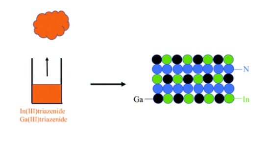
  • Here, an alternative method to depositing ternary materials by introducing both metal precursors with a single pulse. This renders mixing of the metals in both the growth direction and in the growth plane. This was achieved by mixing and co-subliming two solid metal precursors into the ALD chamber.


Wednesday, May 5, 2021

EMD Electronics Creates Center of Excellence for Atomic Engineering by Combining Thin Films R&D Lab with Intermolecular

  • Unique capabilities with novel organo-metallic precursors and applications will enable customers to explore and test advanced materials for next-generation devices
  • Centralized innovation hub to speed up the delivery of material solutions to customers
San Jose, Calif., May 04, 2021 – EMD Electronics, a business of Merck KGaA, Darmstadt, Germany, today announced the creation of a Center of Excellence for atomic engineering at Intermolecular’s San Jose facility. The capabilities of EMD Electronic’s Thin-Films Applications R&D lab have been merged with Intermolecular’s advanced electronics capabilities to create a centralized innovation hub for our customers. This will enable seamless integration of testing and deposition of new materials for next-generation devices.


EMD Electronics "We've established a Center of Excellence for Atomic Engineering! Our  Thin Films Applications R&D lab has merged with Intermolecular's advanced electronics capabilities to create a centralized innovation hub for our customers. This will enable seamless integration of testing and deposition of new materials for next-generation semiconductors." (Quote and photo above from EMD Electronics LinkedIn Announcement LINK)

“Intermolecular’s 150,000 sqft facility in the heart of Silicon Valley is the perfect center to converge materials innovation and testing for our global customers,” said Anand Nambiar, Head of Semiconductor Materials business unit at EMD Electronics. “To continue scaling down to advance nodes and develop next-generation applications, a reliable supply of innovative materials is required. Our expertise in atomic engineering in combination with Intermolecular’s unique tools and processes, will enable our customers to test, validate, prototype and introduce new advanced technologies and materials faster in the market.”

“Ongoing miniaturization drives our customers to build their devices from the atoms up in complex 3D arrangements. Our advanced deposition materials allow them to create differentiation in their products,” said Casper van Oosten, Business Field Head and Managing Director for Intermolecular, Inc. “Until now, the value chain process to test and validate materials involved multiple steps and was time consuming. By combining capabilities, we now have access to the right team, tools and data and can provide our customers with a more seamless integration to prove new organometallic materials for electronic applications.”

On March 4, Merck KGaA, Darmstadt, Germany moved the Silicon Valley Innovation Hub to San Jose’s Intermolecular site creating a unique space for innovation and collaboration with start-ups at the intersection of life science, healthcare and electronic materials. The building boasts 30,000 square feet of cleanroom, chemical labs, offices, a collaboration area and event spaces. Intermolecular, Inc. (“Intermolecular”) is the trusted partner for materials innovation and a wholly-owned subsidiary of the EMD Electronics business of Merck KGaA, Darmstadt, Germany.

About EMD Electronics

EMD Electronics is the North America electronics business of Merck KGaA, Darmstadt, Germany. EMD Electronics’ portfolio covers a broad range of products and solutions, including high-tech materials and solutions for the semiconductor industry as well as liquid crystals and OLED materials for displays and effect pigments for coatings and cosmetics. Today, EMD Electronics has approximately 2,000 employees around the country with regional offices in Tempe (AZ) and Philadelphia (PA). For more information, please visit www.emd-electronics.com.

About Intermolecular

Intermolecular is a trusted partner for materials innovation and the Silicon Valley science hub of Merck KGaA, Darmstadt, Germany and its electronics business. Intermolecular explores, tests and develops advanced materials that are revolutionizing the next generation of electronics that make lives easier, entertaining and more productive. For more than 15 years, the team, methodologies and quality data have driven impactful outcomes, market opportunities and innovative product designs for customers.

About Merck KGaA, Darmstadt, Germany

Merck KGaA, Darmstadt, Germany, a leading science and technology company, operates across healthcare, life science and electronics. Around 58,000 employees work to make a positive difference to millions of people’s lives every day by creating more joyful and sustainable ways to live. From advancing gene editing technologies and discovering unique ways to treat the most challenging diseases to enabling the intelligence of devices – the company is everywhere. In 2020, Merck KGaA, Darmstadt, Germany, generated sales of € 17.5 billion in 66 countries.

The company holds the global rights to the name and trademark “Merck” internationally. The only exceptions are the United States and Canada, where the business sectors of Merck KGaA, Darmstadt, Germany operate as EMD Serono in healthcare, MilliporeSigma in life science, and EMD Electronics. Since its founding 1668, scientific exploration and responsible entrepreneurship have been key to the company’s technological and scientific advances. To this day, the founding family remains the majority owner of the publicly listed company.

Thursday, April 8, 2021

Pegasus Chemicals announce a new supply site in The EU in Sweden

UK ALD and CVD Precursor supplier Pegasus Chemicals announce a new supply site in Europe in Värmdö, Sweden Pegasus Chemicals AB thru a long-term collaboration with Fab Support AB - the biggest supplier of CVD and ALD precursor in North Europe. The location is very close to BALD Engineering HQ also in Värmdö! Welcome to Sweden and Värmdö in the Stockholm Archipelago!


ALD/CVD Metal Precursors US$640M Market Booming to US$910M in 2024

San Diego, CA, April 1, 2021: TECHCET—the electronic materials advisory firm providing business and technology information—announces that the global market for atomic layer deposition (ALD) and chemical vapor deposition (CVD) metal precursors for semiconductor manufacturing in 2020 was worth ~US$640M. Driven by advanced logic and 3D-NAND memory chip fabrication needs, demand for ALD and CVD metal precursors is forecast to see a 2020-2024 compound annual growth rate (CAGR) of ~10% as shown in the Figure (below) from the most recent quarterly update to TECHCET's Critical Materials Report (CMR) on CVD, ALD, and SOD Precursors.


All ALD/CVD metal precursors are in healthy demand since ALD is critical for fabs running 22-45nm nodes as well as for fabs at the leading edge. In particular, cobalt (Co) and hafnium (Hf) precursors saw 18-20% year-over-year (YoY) growth in 2020, and are forecasted to see strong demand through 2024.

Critical Materials Reports™ and Market Briefings: https://lnkd.in/gH6UN8T

For more information: https://lnkd.in/g332mfz

Wednesday, April 7, 2021

Ascensus acquires a global leader in high-purity specialty chemicals and CVD/ALD precursors Strem Chemicals, Inc.

Bellevue, WA, April 7, 2021 – Wind Point Partners (“Wind Point”) and Ascensus Specialties LLC (“Ascensus”) today announced that Ascensus has completed the acquisition of Strem Chemicals, Inc. (“Strem” or the “Company”). Strem is a global leader in high-purity, research-grade catalysts, ligands, organometallics, metal carbonyls and CVD/ALD precursors.


Based in Newburyport, Massachusetts, Strem sells and manufactures specialty chemicals for the most demanding, high-purity end markets of life sciences, microelectronics and other specialties markets. Founded in 1964 by Michael Strem, the Company’s products serve as critical components for manufacturers, researchers and academics. In addition, Strem provides custom synthesis and cGMP manufacturing services for high-potency APIs (active pharmaceutical ingredients).

Headquartered in Bellevue, Washington, Ascensus is the world leader in borohydride, borane, and specialty alcoholates production. Wind Point built Ascensus through the acquisitions of former Dow Chemical and BASF specialty chemicals businesses. Ascensus’ specialty chemicals are essential reagents for life sciences, microelectronics and other specialties customers across North America, Europe and Asia.

Mike Huff, CEO of Ascensus, stated, “We are extremely excited to have Strem join the Ascensus family. Strem has a world-class team and a renowned reputation that has been methodically fostered for over half a century under the leadership of Michael Strem and Ephraim Honig. We will look to further support the team’s highly technical R&D culture, differentiated product offering and value-added customer relationships. Together, Ascensus and Strem will be a global specialty chemicals leader serving the demanding, high-growth life sciences and specialties markets.”

Alex Washington, Wind Point Managing Director, added, “Strem represents an excellent addition to the Ascensus platform. The combined business will have capabilities to offer solutions ranging from lab to large scale commercial production. Strem’s industry-leading technical competency is a meaningful addition to Ascensus’ existing capabilities, and Ascensus looks forward to working with Ephraim and the Strem team to amplify new product and application development efforts.”

Ephraim S. Honig, former CEO of Strem, will be joining the Ascensus leadership team as Chief Science and Innovation Officer and will oversee the combined businesses’ Research and Development function. Mr. Honig noted, “We are excited to become part of the Ascensus family and begin the next chapter for our employees, customers and partners. Ascensus and Strem have highly complementary chemistry capabilities and end market applications. We look forward to accelerating our investment in R&D capabilities to drive innovation and new chemistries on behalf of our customers.”

Michael Strem, Founder & President of Strem Chemicals, commented, “We thoughtfully chose Ascensus as the partner for the next phase of Strem’s growth. Our employees’ interests and well-being have been my top priority, and the strong cultural fit will provide opportunities for our team. The additional resources and global reach of Ascensus will deliver Strem’s strong capabilities to an even broader audience of customers."

Reed Smith LLP served as legal counsel to Wind Point and Ascensus, and KPMG LLP provided advisory services in connection with the transaction. Honigman LLP served as legal counsel and Grace Matthews, Inc. served as financial advisor to Strem.

Friday, March 5, 2021

EMD Performance Materials announces further investments of electronics business and new name: EMD Electronics

  • New name reflects the product and service portfolio designed to enable the future of electronics in a data-driven world
  • Investment into R&D and innovation centers in Tempe and Silicon Valley
EMD Performance Materials today announced an expanded focus on the US electronics business and a new name in the US: EMD Electronics. EMD Electronics, a business of Merck KGaA, Darmstadt, Germany, includes a broad portfolio of semiconductor materials, semiconductor delivery systems and services, display, and surface solutions. The Electronics business globally employs more than 7,400 – with a third of employees in the US across 29 sites, with plans for continued growth in planarization and thin films organizations following recent investments. More information about the Electronics business can be found here.


Additionally, the company announced the relocation of the Silicon Valley Innovation Hub from Menlo Park to Intermolecular's San Jose facilities, combining Merck KGaA, Darmstadt, Germany's innovation efforts in the Bay area with Intermolecular's services for materials and electronics, creating a unique space that empowers collaboration with startups. This announcement follows the $22 million investment at the EMD Electronics site in Tempe, Arizona for its R&D and production for semiconductor materials announced in February.


"Our name change and investment in these centers demonstrate our commitment to continued innovation in electronics and supporting US customers' requirements for capitalizing on growing opportunities driven by digital transformations and data-driven electronics," said Jeff White, President of EMD Electronics. "Our customers are working on cutting-edge technologies and products that range from better immersive displays and surfaces in cars and consumer electronics to how to move neuromorphic and quantum computing to the next level. Our combined expertise and portfolio in display and surface innovations, semiconductor materials and the safe delivery and storage of speciality chemicals and gases will enable new discoveries and novel products not even imagined yet."

As the company behind the companies advancing digital living, the Electronics business sector is involved in all major technology trends – be it 5G, Big Data, autonomous driving, artificial intelligence, or the Internet of Things. Thanks to these and other megatrends, the demand for ever smaller, faster and more energy-efficient electronics is continuously growing. Sample innovations enabled by EMD 

Electronics include:
  • Patterning, deposition and spin-on dielectrics materials to make 3D NAND possible
  • DSA – revolutionary way of building microchips of the future
  • OLED for brighter, thinner, free-form displays
  • Liquid crystals for electronic steerable antennas to bring connectivity to places currently not reachable
  • eyerise ® liquid crystal for greener windows and innovative building architecture
These technologies and innovations are being implemented across a diverse set of customers including larger companies and start-up companies. To enable new inventions for start-ups, EMD Electronics has launched a program for early-stage and growth companies looking to advance their technologies in the areas of displays, semiconductor materials, neuromorphic computing, AI enabled materials development and smart manufacturing by applying for the EvoNexus MarketLink Program by March 12.

Monday, March 1, 2021

Welcome to the RASIRC ALD Oxide Wizard

Welcome to the RASIRC ALD Oxide Wizard. The wizard compares the reactivity of water and hydrogen peroxide for 285 different precursors.
  • Direct theoretical comparison between water and hydrogen peroxide
  • Allows for rapid screening of possible precursors
  • Allows for lower cost precursors to be used where previous water reactivity was too low
  • Allows for visualization of precursors to better understand steric hindrance effects
Starting with the five of the most common metals used in Atomic Layer Deposition (ALD) and 57 common ligands, the wizard creates the desired precursor, visualizes the precursor molecule, and concludes with a determination of reaction energetics (favorable/less favorable) in terms of intrinsic energy changes ∆E added or released in the creation of the metal oxide with H2O2 or water. The wizard allows you to make modifications to the ligand and see the effects on reactivity. Edit your design as many times as you want; when you have your desired reaction, choose the print option.

Enter The RASIRC ALD Oxide Wizard HERE!


Example using the HfI4 H2O vs H2O2 going from -30.3 to -180.5 kJ/mol - The more negative the value, the more thermodynamically likely the reaction is to occur.


Tuesday, February 23, 2021

Thermal Atomic Layer Deposition of Gold: Mechanistic Insights, Nucleation, and Epitaxy

Here is a new paper with deep insights into thermal ALD of gold from Argonne National Lab in the USA. They are using the previously developed precursor from Mikko Titalas ALD group at Helsinki University Finland Me2Au(S2CNEt2). All depositions were carried out in a Veeco CNT Savannah reactor.

Thermal Atomic Layer Deposition of Gold: Mechanistic Insights, Nucleation, and Epitaxy

Pengfei Liu, Yuchen Zhang, Cong Liu, Jonathan D. Emery, Anusheela Das, Michael J. Bedzyk,
Adam S. Hock*, and Alex B. F. Martinson*
ACS Appl. Mater. Interfaces 2021, XXXX, XXX, XXX-XXX
Publication Date:February 9, 2021https://doi.org/10.1021/acsami.0c17943

An in situ microbalance and infrared spectroscopic study of alternating exposures to Me2Au(S2CNEt2) and ozone illuminates the organometallic chemistry that allows for the thermal atomic layer deposition (ALD) of gold. In situ quartz crystal microbalance (QCM) studies resolve the nucleation delay and island growth of Au on a freshly prepared aluminum oxide surface with single cycle resolution, revealing inhibition for 40 cycles prior to slow nucleation and film coalescence that extends over 300 cycles. In situ infrared spectroscopy informed by first-principles computation provides insight into the surface chemistry of the self-limiting half-reactions, which are consistent with an oxidized Au surface mechanism. X-ray diffraction of ALD-grown gold on silicon, silica, sapphire, and mica reveals consistent out-of-plane oriented crystalline film growth as well as epitaxially directed in-plane orientation on closely lattice-matched mica at a relatively low growth temperature of 180 °C. A more complete understanding of ALD gold nucleation, surface chemistry, and epitaxy will inform the next generation of low-temperature, nanoscale, textured depositions that are applicable to high surface area supports.


Tuesday, January 12, 2021

Semiconductor Materials $50B Market on a Strong Run in 2021

Semiconductor Materials $50B Market on a Strong Run in 2021Pandemic pushing people to Work From Home and School From Home

San Diego, CA, January 12, 2021: TECHCET announced that global revenues for semiconductor manufacturing and packaging materials grew approximately 4% year-over-year (YoY) in 2020 to ~US$50B, and are expected to grow ~7% in 2021 to nearly US$54B. The COVID-19 pandemic has created strong demand for both logic and memory ICs to support Work From Home (WFH) and School From Home (SFH), and such demand is expected to increase despite expanding availability of virus vaccines. Also, demand for automotive ICs has recovered and will be an important driver in 2021 growth. The compound annual growth rate (CAGR) through 2024 is forecast at 5.3% as per the latest TECHCET Critical Materials Reports (CMR) and shown in the attached figure.

Analysts' Alerts emailed to CMR purchasers help them anticipate and mitigate potential supply-chain disruptions. Excerpts have been publicly disclosed on the following critical materials (https://lnkd.in/dzAZcCw):

* IPA in "CMC Considers Bio-Solvents to Reduce Fab Risks",
* HF in "Semi Wet Chemicals US$2B Market Threatened by Localization", and
* Lanthanum in "Rare Earth Elements (REE) Supply Uncertain for IC Fabs".


Thursday, December 17, 2020

Low Resistivity Titanium Nitride Thin Films ALD realized by RASIRC Brute® Hydrazine vaporization technology

TiN ALD is one of the most important ALD processes in high volume manufacturing in the semiconductor industry for more than 15 years. Most Tier 1 ALD equipment manufacturers (e.g. ASM International, Tokyo Electron , Applied Materials, Lam Research, Kokusai, Jusung Engineering, Wonik IPS, Picosun) has TiN ALD and PEALD in their process portfolio for 300 mm wafer productions targeting the Logic, 3DNAND and DRAM fab customers (e.g. Intel, Samsung, TSMC, SK Hynix, Micron, Globalfoundries, Toshiba, TI) because the metallic film has proven to be highly flexible metal film due to:

  • Relatively cheap precursor, mainly TiCl4 and TDMAT, as compared to the much more expensive precursors with lower vapor pressure for tantalum metal nitrides (PDMAT) and metals like Co (CCTBA) and Ru (RuCp´s). 
  • High vapor pressure and reactivity allowing fast conformal processing bay both CVD, pulsed CVD and ALD for TiCl4/NH3 based processes 
  • Possibility to tune low resistivity films however at relatively high temperatures (TiCl4/NH3) not allowing for BEOL thermal budget requirements (<390 °C) 
  • Excellent barrier properties hindering metal diffusion (TDMAT and TiCl4) 
  • Metal gate work function tuning by doping and partial controlled oxidation 
  • Oxygen gettering driving excess oxygen from the gate oxide channel interface into the metal gate reducing the CMOS device EOT. 
  • Mini Batch and Large Batch processing capability (e.g. TEL Indy, ASM A412, Kokusai ALDina, Picosun Sprinter)

Due to low resistivity, titanium nitride (TiN) thin films are in production as the diffusion barrier for Cu, Co and W as well as the gate metal barrier in CMOS. However, as mentioned, for high aspect ratio features, thermal ALD deposition  is needed because of high conformality. Therefore, it is very important to develop thermal ALD TiN processes further to improve the capacitor electrode, barrier and CMOS metal gate properties to perfection.


Cheng-Hsuan Kuo and co-workers at UCSanDiego in the Kummel research group, has recently concluded a study on TiN ALD utilizing the RASIRC BruteÒ Hydrazine (N2H2) vaporizer technology, which is presented this week at IEEE SISC December 16-18 (LINK).

In the work, titanium tetrachloride (TiCl4) and anhydrous hydrazine (Rasirc, Brute HydrazineÒ) were employed as the precursors with ultra-high purity nitrogen purge gas.

  • The TiN ALD chamber was connected to an in-vacuo Auger Electron Spectrometer (RBD Instruments), which was used to determine the atomic composition of ALD. (Fig. 1)
  • The sample was biased at -100V DC and Ar plasma (50W) was used to remove the surface oxides and impurities. (Fig. 2)
  • To determine resistivity, four-point probe (Ossila) measurements were performed on TiN thin films on degreased SiO2 substrates. (Fig. 3)
  • Scanning electron microscopy (SEM), ellipsometry, and X-ray reflectivity (XRR) were used to measure TiN film thicknesses. (Fig. 4)


Fig.1 Auger Electron Spectroscopy of TiN at different sputtering time.(oxygen and carbon contents are listed)


Fig. 2 Oxygen concentration and resistivity vs pulse length at 300 °C 


Fig. 3. Oxygen concentration and resistivity vs pulse length at 350 °C 


Fig.4 X-Ray Reflectivity (XRR) of the 350 oC TiN film with optimal pulse lengths 

To conclude, these experiments indicate that minimizing oxygen concentration is key in producing TiN thin films with desirable electrical properties.

The optimal resistivity of the TiN deposited at 350oC was 160 micro-ohm-cm which is the lowest reported resistivity of any TiN film deposited by thermal ALD.  As stated above the importance of 3D process capability can be met by having TiN thin films synthesized by using thermal ALD and post-plasma treatment reducing oxygen concentration and impurities potentially in very high aspect ratio structures such as contact holes, FinFET, Gate all around FETs, vias, DRAM capacitors structures as well as 3DNAND metal gates and contacts.

References

[1] C. H. Ahn. et al. Metals and Materials International, 7 (2001)

[2] Steven Wolf et al. Applied Surface Science 462 (2018)

Acknowledgements

This work was supported in part by the SRC

LINKS

UCSanDiego 

Kummel research group

EEE SISC December 16-18 (LINK).


Friday, November 6, 2020

Refreshing Material Advances for Logic, Memory, and Packaging5th CMC Conference "After-Hours" Available up to December 11

How to keep semiconductor fabs supplied with critical materials despite a pandemic and trade wars was discussed by >250 industry experts gathered in virtual space October 21-22 during the 5th annual Critical Materials Council (CMC) Conference. CMC Fab Members and Associate Supplier Members were joined by leading industry analysts, educators, and investors in discussing business and technology trends in the value-chain for advanced packaging, logic, and memory. The "after-hours" virtual conversations will continue through December 11th using the conference app and website, and new people can join in through November 16th.

"There were a lot good topics especially on materials challenges for leading edge technology and heterogeneous integration, global issues on material supplies, and emerging materials development," commented Dr. Lihong Cao, Director of Engineering and Technical Marketing at ASE, and Session 4 presenter.


Dr. Lauren Link of Intel discussed the need to find ways to integrate more front-end fabrication materials into packaging. The challenge is doing so in a cost-effective manner, without over-specifying materials and process requirements.

CMC-Oregon-Header

5th Annual CMC Conference "After-hours" Starting Now!

Didn't Catch the Conference "Live"? No Worries! Register Today and Get Access to the recordings, Connect attendees, Engage in Q&A!

Registration Open until November 16

Access Presentations thru December 12

Thursday, October 29, 2020

Researchers develop new atomic layer deposition process using ultrasonic precursor evaporation

ALD community's creativity has not been saturated. A new Ultrasonic Atomization technology based ALD has been developed:

A new way to deposit thin layers onto a substrate material at near room temperatures has been invented at The University of Alabama in Huntsville (UAH), a part of the University of Alabama System. UAH postdoctoral research associate Dr. Moon Hyung Jang got the idea to use an ultrasonic atomization technology to evaporate chemicals used in atomic layer deposition (ALD) while shopping for a home humidifier.

The UAH scientists' ultrasound invention makes it possible to use a wide range of reactive chemicals that are thermally unstable and not suitable for direct heating. Ultrasonic atomization supplies low vapor pressure precursors because the evaporation of precursors was made through ultrasonic vibrating of the module.


While observing how a home humidifier works, Dr. Moonhyung Jang got the idea to use an ultrasonic atomization technology to evaporate chemicals used in atomic layer deposition and worked with Dr. Lei to develop and test the device. (Photo credit: Michael Mercier / UAH)

The process uses a piezo-electric ultrasonic transducer placed in a liquid chemical precursor. Once started, the transducer starts to vibrate a few hundred thousand times per second and generates a mist of the chemical precursor. The small liquid droplets in the mist are quickly evaporated in the gas manifold under vacuum and mild heat treatment, leaving behind an even coat of the deposition material.

Source: UAH LINK
----------
By Abhishekkumar Thakur

Monday, August 3, 2020

BDEAS - a versaitile ALD precursor for high quality dilectric films in leading edge semiconductor applications

One of the most important reasons why Silicon (Si), in place of Germanium (Ge), was propelled to the front of the class in the semiconductor industry from the very beginning, is the fact that Si forms a very stable oxide-semiconductor interface with SiO2. A high-quality oxide interface is a key to making field-effect transistors (MOSFETs). Germanium oxide is water-soluble which rendered it useless for MOSFET fabrication in the early days (now the industry is advanced enough to possibly solve that).

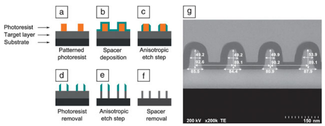
Thermal oxidation of Si at temperatures > 800 °C yields SiO2. To avoid such high temperatures and long processing times and tune the material properties, (wet) chemical oxidation, (plasma-enhanced) chemical vapor deposition or sputtering and electron beam evaporation are also preferred methods to grow SiO2. The advantages of precise thickness control, optimal large-area uniformity, and the conformality over demanding substrate topologies of atomic layer deposition (ALD) based SiO2 films, all led to an expansion of target applications such as; spacer based self-aligned double/quadruple patterning (SADP or SAQP) in fabricating DRAM and logic chips (Link), interface engineering between Si and high-k materials (Link), moisture barrier or protective or insulator coatings (Link), nanolaminate structures with tailored optical and electronic properties (Link) and double layer surface passivation in Si photovoltaics (Link), etc. to name but a few.


Link for the image

Bis(diethylamino)silane (BDEAS) [SiH2[N(CH2CH3)2]2, also known as SAM-24[MP1] , is one of the most preferred Si precursors for ALD of SiO2 and other Si-containing films. It’s an air-sensitive, moisture-sensitive, flammable, colorless, and odorless liquid precursor (boiling point 70 °C (30mm), density 0.804), which exhibits a high vapor pressure, i.e. ~100 Torr at 100 °C.

The research group of Prof. W. M. M. Kessels, Department of Applied Physics, Eindhoven University of Technology, has reported that BDEAS is suited for low-temperature synthesis of high-quality SiO2 by ALD with the SiO2 properties being relatively insensitive to the substrate temperature for the temperature range of 100 – 300 °C; for temperatures reaching 400 °C thermal stability issues of the precursor and its ligands start to play a role. The process is also relatively fast as it combines a high growth-per-cycle (0.8 – 1.7 Å/cycle) with relatively short dosing and purge times. The ALD SiO2 processes with BDEAS precursors are therefore of interest for high-volume manufacturing applications, for instance, using ALD batch processes or inline (plasma) ALD equipment.

Link for the image

Strem Chemicals, Inc., a high purity specialty chemicals manufacturer and supplier, headquartered in Newburyport, Massachusetts, USA, boasts a vast variety of ALD/CVD precursors, including BDEAS for depositing Si-based films in different applications.

Since 1964, Strem Chemicals, Inc. has been serving its clients from academic, industrial, and government research and development laboratories as well as commercial scale businesses in the pharmaceutical, microelectronic, and chemical/petrochemical industries. Strem also provides custom synthesis (including high-pressure synthesis) and current good manufacturing practice (cGMP) services. With ISO 9001 certification for the Quality Management System (QMS) standard and documentation, Strem products are high purity materials, typically 99%, with some at 99.9999% metals purity. Strem utilizes a comprehensive range of analytical techniques tailored to each product to ensure quality because  researchers typically rely on the supplier's quality procedures and documentation, which if poorly conducted[MP1]  may kill a great research idea. All of Strem's catalogs, since inception, have listed “Color and Form” for every product as primary indicators of quality.


 [MP1]SAM-24 may be an Air liquide trademark.

----------

Promotional blog written and researched by Abhishekkumar Thakur and Jonas Sundqvist, BALD Engineering AB