Showing posts with label LED. Show all posts

Tuesday, April 23, 2019

Micro-LEDs achieve superior brightness with Picosun’s ALD technology

ESPOO, Finland, 23rd April 2019 – Picosun Group, supplier of the leading AGILE ALD™ (Atomic Layer Deposition) thin film coating solutions, reports superb results in boosting micro-LED performance using ALD passivation. 
 
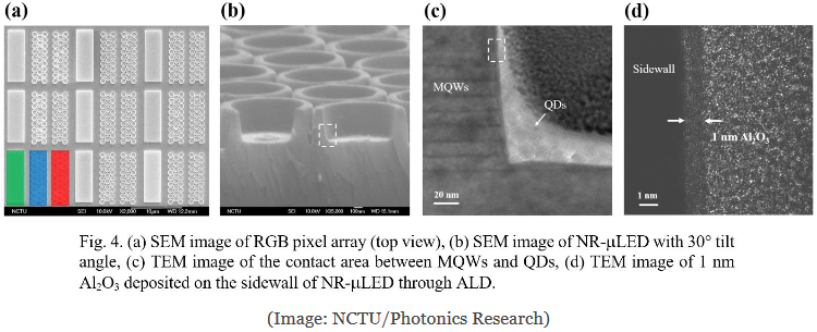
Researchers from Taiwan’s National Chiao Tung University, China’s Xiamen University and SIJ Technology have developed a monolithic Micro LED which achieves full-color display. Through the adoption of ALD, the thin layer between multiple quantum wells and quantum dots of NR Micro LED can be controlled and nonradiative resonant energy transfer (NRET) for color conversion can be maintained (LINK).
 
Micro-LEDs are a strong challenger to existing display technologies such as LCDs (liquid crystal displays), OLEDs (organic light-emitting diodes) or conventional LEDs (light-emitting diodes). Offering compact size, low power consumption, superior brightness, and energy efficiency, higher contrast and color saturation, ultra-high resolution, flexibility, and excellent reliability, micro-LEDs are currently actively studied and developed at the leading electronics manufacturers and R&D institutes around the world. Micro-LEDs are typically used for small screens such as those used in tablets, smartphones, and smartwatches, and the first large area displays have also been demonstrated already.


The Co-Lab collaboration signature ceremony of NCTU and Finland Picosun 2015 (LINK)
 
Still, the micro-LED technology has certain drawbacks that hinder its full-scale commercial breakthrough. The micro-LED screen consists of minuscule pixels producing green, blue and red light. Some steps in the manufacturing process of these pixels easily cause damage to their delicate nanometer-scale structures, which leads to loss of light intensity. ALD has now been proven to effectively fix these damages, not only restoring the light intensity but actually boosting it to superior levels. At Picosun customer site, National Chiao Tung University (NCTU), Taiwan, the light-emitting intensity of micro-LEDs has been enhanced by 143.7% by using ALD passivation layers deposited with PICOSUN™ ALD equipment(*).

“We are happy to report these great results achieved in micro-LED efficiency enhancement using ALD technology. PICOSUN™ ALD equipment has been an integral part of our facilities for a long time, and we are always impressed by their performance and the superior ALD film quality obtained with them. Picosun’s customer support is also impeccable, which is very much appreciated considering we collaborate extensively with industries. Whenever we need something regarding the equipment or process consultancy, Picosun staff is always up to date and ready to provide thorough answers,” states Professor Hao-Chung Kuo from NCTU.

“NCTU is our prestigious customer and a key partner for years already. We are glad that our ALD solutions have enabled this impressive performance boost to their micro-LEDs. Micro-LED technology has immense potential to disrupt the solid-state lighting market and our Asian customers, both in industries and R&D, will surely lead the forefront of this development,” continues Mr. Edwin Wu, CEO of Picosun Asia Pte. Ltd.

Saturday, January 26, 2019

Oxford Instruments Partners ITRI for Micro LED Development with Plasma Etch Solutions

[LED Inside, LINK] Oxford Instruments Plasma Technology (OIPT) announced that it has worked with Taiwan’s Industrial Technology Research Institute (ITRI) by providing multiple PlasmaPro 100 systems including both etch and deposition for ITRI’s Micro LED R&D program.

 
The PlasmaPro 100 ICP process solutions are designed to support leading edge device applications such as Lasers, RF, Power and advanced LEDs.

Thursday, October 25, 2018

NCD contracted to supply new ALD equipment for production of µ-OLED with LG Display

Korean ALD equipment manufacturer, NCD reports new order of µ-OLED ALD equipment from LG Display

"NCD has recently contracted with LGD to supply µ-OLED manufacture equipment which is new Lucida GuD Series for Al2O3-ALD encapsulation to avoid OLED degradation induced water and oxygen. Newly introduced Lucida GuD is high volume batch-type ALD equipment based on the process and hardware of OLED encapsulation technology of Lucida GD Series.

µ-OLED produced by this system is micro display with high resolution for augmented reality(AR) and virtual reality(VR) and has been expected the huge application and market in the future.

Otherwise, manufacture of µ-OLED requests high productivity like display industry therefore ALD tools with high film quality and low throughput for Semiconductor couldn’t meet the need of the customers and the market. So NCD is more expecting that this µ-OLED is next growth engine market because it has high volume ALD equipment and excellent OLED encapsulation technology.

NCD will lead µ-OLED ALD equipment market with this starting point and continue to make efforts to become the world’s best specialized ALD technology company.”


LucidaTM GuD Series


Wednesday, January 10, 2018

Osram orders multi-reactor Propel HVM and K475i MOCVD systems from Veeco for high-volume photonics and LED applications

Epitaxial deposition and process equipment maker Veeco Instruments Inc of Plainview, NY, USA says that Osram Opto Semiconductors GmbH of Regensburg, Germany has ordered a multi-reactor Propel High-Volume Manufacturing (HVM) gallium nitride (GaN) metal-organic chemical vapor deposition (MOCVD) system, as well as K475i MOCVD systems. 

The K475i system incorporates Veeco’s Uniform FlowFlange technology, producing films with very high uniformity and improved within-wafer and wafer-to-wafer repeatability with what is claimed to be the industry’s lowest particle generation for demanding applications like photonics and advanced LEDs.  

Source: Semiconductor Today LINK


Incorporating proprietary TurboDisc and Uniform FlowFlange™ MOCVD technologies, the new K475i system enables Veeco customers to reduce LED cost per wafer by up to 20 percent compared to alternative systems through higher productivity, best-in-class yields and reduced operating expenses. (Source: Veeco LINK)

Saturday, August 19, 2017

OSRAM Opto Semiconductor Acquires MOCVD Systems from AIXTRON

AIXTRON announced that OSRAM Opto Semiconductors has purchased the company's AIX 2800G4-TM Planetary system for the manufacturing of mainly infrared-based high power lasers and LEDs based on gallium arsenide (GaAs).

Source: LEDinside LINK
Photo credit: Aixtron (www.aixtron.com)
From Aixtron Press release: “We are very pleased that OSRAM Opto Semiconductors has selected our AIX 2800G4-TM platform for the production of high power laser and infrared LED devices. Their trust in our AIX 2800G4-TM system confirms our strategy to focus on solutions for the most demanding applications, where superior process performance is mandatory to meet our customer’s requirements. Following the recent qualification of our AIX G5 C platform and achieving this key milestone also with the AIX 2800G4-TM, we are looking forward to further deepen our partnership with one of the most innovative semiconductor manufacturers worldwide”, explains Dr. Frank Schulte, Vice President AIXTRON Europe.

Sunday, February 12, 2017

Osram Opto and Picosun improving the properties of LEDs in joint EU Project FLINGO

The FLINGO project: an international team of experts is improving the properties of LEDs

Osram Opto Semiconductors is coordinating the project with four partners from industry and research


In view of the growing demands placed on the electrical, optical and thermal functionality of LEDs, more and more attention is being paid to research into new material properties. The purpose of the FLINGO project is therefore to develop new materials (layers in particular) and processes to improve the characteristics of LEDs, such as efficiency and durability. The intention is to maintain and improve market leadership in innovative LED products. As the project coordinator, Osram Opto Semiconductors is working since February 2017 with renowned universities, research institutes and companies. The German Federal Ministry for Education and Research is sponsoring the FLINGO project (Functional Inorganic Layers for Next Generation Optical Devices) as part of the M-ERA.NET EU initiative. 
 

In the course of the FLINGO project different deposition methods for thin films such as atomic layer deposition, spray pyrolysis and the sol gel process for manufacturing high-quality LED light sources are to be investigated and combined. Under the leadership of Dr. David O’Brien from Osram Opto Semiconductors, the project partners will be working on the entire bandwidth of new component properties – including extended lifetime, smaller electrical layer resistance and improved light extraction. These require new materials and innovative or adapted deposition processes. “The project objectives can only be achieved with the assistance of a broad-based consortium because they call for improvements, new developments and especially expert know-how across the entire value added chain”, explained O’Brien. 

Interdisciplinary expertise from five project partners

The members of the FLINGO project in addition to Osram Opto Semiconductors as the coordinator are Uninova from the New University of Lisbon, the Finnish thin film technology company Picosun Oy, the Fraunhofer Institute for Silicate Research ISC in Würzburg and Vilnius University. Fraunhofer ISC provides support with its know-how in the development of new inorganic layer systems which are to be used as the matrix for sensitive converter materials. Uninova adds its expertise in the manufacture of highly transparent and highly conductive layers which are needed for the p-contact in the LEDs. Picosun Oy is developing atomic layer deposition (ALD) processes and new materials to ensure conformal coating of even heavily structured surfaces. The Institute for Applied Research at Vilnius University provides specialist knowledge in the development and characterization of non-destructive material properties and will analyze the new layers and layer systems developed in the FLINGO project. As an end user of the technologies developed in FLINGO, Osram Opto Semiconductors will ultimately transfer the new thin layers and layer systems to its LEDs to test them for their suitability for the mass market. “The results of the project should lead to highly efficient and durable white light LEDs with possible applications in general lighting for example”, added O’Brien. “Our intention here is to improve our competitiveness and that of European industry in this field.”

FLINGO will be sponsored throughout its intended duration until January 2020 by the German Federal Ministry of Education and Research as part of the M-ERA.NET EU program. M.ERA.NET is an EU-financed network set up to support the coordination of European research projects. You can find more information on M.ERA.NET here.

Friday, June 19, 2015

IKEA invests in French GaN on Silicon LED lighting technology

As reported by Electronics Weekly : Ikea’s venture capital arm has invested in a French firm developing and manufacturing 3D LEDs. Grenoble-based Aledia is developing LEDs for lighting based a gallium-nitride-on-silicon technology.


Two years after it began phasing out incandescent bulbs, Swedish retailer Ikea announced that it is taking another step and planning to sell only energy-efficient LED lighting by 2016.


Ikea believes there is this low-price LED lighting technology for residential use has the potential of faster implementation of the LED technology, leading to savings for customers.


Christian Ehrenborg, managing director of Ikea GreenTech AB, said:

“This technology will be one important part in the IKEA Group strategy to supply high-quality, energy-saving lighting products to consumers worldwide.”


Christian Ehrenborg, Bald guy.

Aledia received the investment from IKEA as part of a €28.4m funding round.

“This financing round, abundantly oversubscribed and particularly the presence of two very large potential corporate customers, testifies to the interest that our cost-disruptive nanowire LED technology is generating in the customer base, as well as in the financial community,” said Giorgio Anania, CEO, chairman and co-founder of Aledia.

Aledia is developing LEDs that are manufactured on 200mm diameter GaN-on-silicon wafers to keep cost down.

Anania said:

“We are progressing with the development of the technology and this financing round will allow us to accelerate significantly the speed of development and the customer traction. In Valeo we have a major potential customer in the automotive LED market, generally viewed as the most profitable market segment. Simultaneously with the investment, we have signed a supply agreement with Valeo.”

The technology was originally developed by CEA-Leti


Fundamental Differences in Planar and 3D LEDs

(Some background information from www.aledia.com)

Conventional LEDs are planar, two-dimensional (2D) devices that emit light from a thin material layer at or near their flat surfaces. They typically are made by depositing multiple layers of various materials, each having different thermal expansion and crystal lattice constants, on small wafers with diameters between 2 inches and 6 inches. The vast majority of LEDs are made of GaN and indium gallium nitride (InGaN) material. Depositing high-quality layers of these materials requires the GaN to be grown on substrate wafers that are made of expensive materials such as sapphire, silicon carbide or gallium nitride, as these materials are closely matched to GaN in terms of thermal expansion coefficient and crystal lattice parameters. Building planar GaN LEDs on larger and less expensive wafers made of silicon – a material that is very different from GaN in terms of thermal expansion and crystal lattice constant – is being tried, but to date this approach has shown only moderate cost savings while often incurring high defect densities, lower performance and lower yields. These factors contribute to the high costs of today’s LEDs.


In contrast, Aledia’s WireLED product technology uses economical silicon wafers with diameters of 8 inches (200 mm) or larger. On each wafer, millions of vertical microwires or microrods of GaN are grown, each with a diameter of less than 1 micron. Each microwire is an LED, capable of emitting light from all sides.


Standard Technology - 2D (Planar) LEDs:
• Small, expensive substrate
• Slow MOCVD growth process (high capital expenditure)
• High materials consumption
• LED-specific manufacturing plants
• Light emission area = at most the 2D area
• Single color on one wafer


3D (Microwire) LEDs:
• Large, economical substrate
• Fast MOCVD growth process (low capital expenditure)
• Low materials consumption
• Existing high-volume silicon wafer fabs
• Light emission area = up to 3X the 2D area = more light/mm2 or less current density, less efficiency droop
• Multiple colors on one wafer or even on one chip


Tuesday, February 3, 2015

University of Manchester slim down LEDs using atom thick materials

Ultrathin, flexible and semi-transparent LEDs made from a mix of different atom thick materials have been created by researchers in the UK and Japan. Beyond their scientific importance, the researchers believe the design could have significant commercial potential. Other researchers agree, but says that a suitable method for producing the devices is still needed.
 

Since graphene's remarkable electrical properties were discovered, other monolayer materials followed whose electrical properties are often very different. While graphene is an excellent conductor, boron nitride is an insulator and some transition metal dichalcogenide (TMDCs) monolayers are semiconductors. Several research groups have developed simple van der Waals heterostructures, such as tunnelling transistors, by combining multiple layers. Now Konstantin Novoselov, who shared the 2010 physics Nobel prize with Andre Geim for their discovery of graphene, and colleagues at the University of Manchester, have produced LEDs using the most complex monolayer heterostructures ever created.
 

Light-emitting diodes by band-structure engineering in van der Waals heterostructures
F. Withers, O. Del Pozo-Zamudio, A. Mishchenko, A. P. Rooney, A. Gholinia, K. Watanabe, T. Taniguchi, S. J. Haigh, A. K. Geim, A. I. Tartakovskii & K. S. Novoselov
Nature Materials(2015) doi:10.1038/nmat4205 Published online 02 February 2015 

The advent of graphene and related 2D materials, has recently led to a new technology: heterostructures based on these atomically thin crystals. The paradigm proved itself extremely versatile and led to rapid demonstration of tunnelling diodes with negative differential resistance, tunnelling transistors, photovoltaic devices, and so on. Here, we take the complexity and functionality of such van der Waals heterostructures to the next level by introducing quantum wells (QWs) engineered with one atomic plane precision. We describe light-emitting diodes (LEDs) made by stacking metallic graphene, insulating hexagonal ​boron nitride and various semiconducting monolayers into complex but carefully designed sequences. Our first devices already exhibit an extrinsic quantum efficiency of nearly 10% and the emission can be tuned over a wide range of frequencies by appropriately choosing and combining 2D semiconductors (monolayers of transition metal dichalcogenides). By preparing the heterostructures on elastic and transparent substrates, we show that they can also provide the basis for flexible and semi-transparent electronics. The range of functionalities for the demonstrated heterostructures is expected to grow further on increasing the number of available 2D crystals and improving their electronic quality.

Heterostructure devices with a SQW and MQWs.

Thursday, November 13, 2014

ALD for Light Emitting LED and OLED by Picosun

From AZ Materials: Over the past few years, the wafer-based semiconductor industry has been using the atomic layer deposition (ALD) thin film coating technique to develop a wide range of electronic products and components. For an improved level of system miniaturization and integration, thin films have to be uniform, dense and conformal, as well as free from pinholes, cracks and other defects.

When the preferred film thickness begins to approach nanometer scale, traditional thin film deposition methods such as PVD and CVD do not meet this requirement. In contrast, ALD forms excellent quality films even on the most complex nanoscale geometries. This can be attributed to its surface controlled and self-saturating film growth mechanism.

LED manufacturing is a wafer-based technology – similar to integrated circuit (IC) device manufacturing techniques. ALD is an optimal method that can be incorporated into current LED manufacturing processes and it can provide a wide range of benefits to the industry, either by introducing new manufacturing steps or replacing existing ones to extend the product lifetime, improve the device efficiency, or to save manufacturing costs.


Picosun’s PICOPLATFORM™ 200 vacuum cluster system for wafers up to 200mm diameter.

Currently a number of LED manufacturers across the globe are using Picosun’s ALD technology in their production. For OLEDs, Picosun delivers excellent ALD solutions to protect the devices against moisture

Full story here