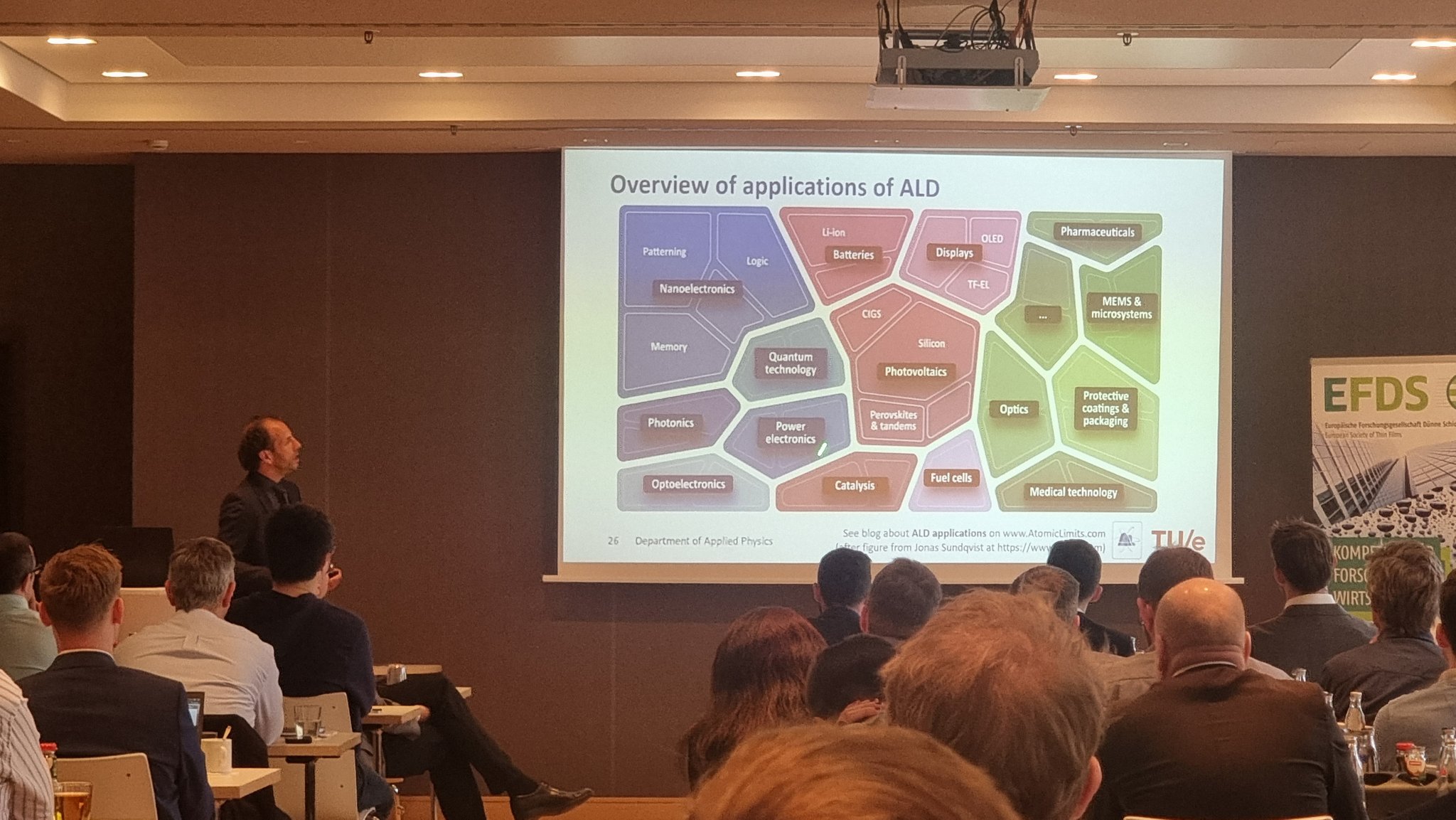
Save the date! On June 9th 2022, we will organize a spatial ALD day at the Eindhoven University of Technology.
— AtomicLimits (@AtomicLimits) April 6, 2022
You can preregister on the website! The final registration form will appear early May when the detailed program is known.https://t.co/GjjpkGRdDX#ALDep #ALD pic.twitter.com/Bt5jJYg111
Header


%20(1).png)
Thursday, April 7, 2022
Spatial ALD Day coming up at TU Eindhoven June 9
Wednesday, April 6, 2022
Senior Process Engineer I- Coating at ASM Phoenix AZ
About the job
We’re not like most. We don’t just overcome obstacles – we don’t see them. Instead, we see the potential in every person, and every situation. We don’t wait for opportunity to appear – we create it. Meet ASM. A company that has been searching for people just like you.
Who is ASM?
ASM is a leading, global supplier of semiconductor wafer processing equipment. Our ambitious team is dedicated to delivering innovative technology solutions to the world’s leading semiconductor manufacturers. We have over 2,600 employees based in 14 countries, including Belgium, Japan, Netherlands, South Korea, Singapore, Taiwan and United States. Together we work to develop Epitaxy, ALD, PEALD, Vertical Furnaces and PECVD thin-film deposition technologies for our customers. Our goal is to remain an industry leader by being ahead of what’s next. We accomplish this by focusing on finding collaborative solutions to make integrated circuits, or chips, smaller, faster and even more powerful.
ASM, an inclusive workplace
We at ASM are a truly global organization that works diligently with an open-mind in all areas of our business. We strive for a culture and work style that fosters trust and transparency. We put our people first, and that is how we will continue to succeed. We are an equal opportunity employer and value diversity. We recognize and value the differences between individuals, including gender, ethnicity, religious beliefs, sexual orientation, knowledge and experience, work background, age, skills, amongst others. Recruiting and developing a diverse workforce provides a wide range of perspectives. This enables a culture of continuously exploring and adopting new technological ideas and innovations, and it also enables us to deliver excellent products and service to our clients.
Essential Functions
- Work with a safety-first mentality
- Drive ASM process protocol with emphasis and regularly institute or update service solutions to the field
- Work on assigned CIP projects, develop DOE’s and communicate openly both internally and externally.
- Focus on refresh of IP for legacy products and influence new design IP.
- Provide “novelty” to items making them hard to reproduce
- Improve upon existing design for performance and cost efficiency
- Generate project scope documentation and prepares specific project reports against identified schedule.
- Building stakeholder consensus to deliver approach
- Collaboratively manages global stakeholders including end users, technicians, engineers, procurement, spares, manufacturing, subject matter experts as well as management in both business and / or operations to project specific details.
- Applies project management principles to produce cooperative and collaborative efforts, deliver business strategic objectives and fill the end customer needs.
- Consistently provide quality solutions to field and customer personnel and create new BKM’s.
- Exercise good judgment within broadly defined practices and policies in selecting methods, techniques, tools and evaluation criteria for obtaining desired results
- Be willing to travel domestically and internationally as required.
- BS or MS Degree in Mechanical engineering, Electrical Engineering, Material Science or related degree required.
- 5+ years of experience in the semiconductor field.
- Equipment Engineering experience with design, and development of complex mechanical systems including comprehension of: reactors, vacuum systems and chambers, gas delivery systems, abatement systems, pneumatics, water cooling, and circuits required. Ability to implement, maintain, improve electrical instruments, equipment, facilities, components, products, systems and provide novel solutions for the semiconductor equipment industry. Comprehension of PLC's and functionality.
- Should have a broad based background in analysis and debug of complex electrical and/or mechanical systems
- Semiconductor capital equipment experience is preferred.
- Understanding of materials: metals, plastics, surface coatings and surface finishes.
- Deposition product knowledge a plus (CVD, ALD, EPI, PVD). Knowledge of ASM Emerald tool distinct plus.
- Design applications Pro/ENGINEER, AutoCAD, and Hands on experience with FEA and CFD analysis preferred. Solid ability to read and understand P&IDs, Electrical, and Mechanical schematics and drawings.
- Proficiency in ANSI Y14.5 geometric dimension and tolerance.
- Ability to rectify a challenging situation and gain customer (Internal and external) confidence
- Strong positive attitude, ability to work in a team environment and work alone. Able to drive meetings, both internal and external, with excellent internal ASM relations
- Ability to work responsibly with all ASM resources and departments in a multifunctional high paced atmosphere with minimum supervision on highly complex problems
- Ability to handle multiple tasks simultaneously and be able to organize and run projects
- Strong computer skills, working knowledge of MS Word, Excel, PowerPoint, SharePoint, Project, and SAP
- Drive ASM SOP’s and protocol, able to guide co-workers toward common goals
- Become an active member of ASM GSS core teams
- Excellent communication skills; speak and write in a clear and concise manner, and ability to accurately and fully convey issues to peers, management, or customers
- Strong organizational skills and leadership qualities
- Accurate, timely reporting
- Parts tracking, ordering, managing, Setting BOM levels
- Technical writing background. Ability to create procedures, written in an informative manner that eliminates ambiguity and personal interpretation
- Training skills, be able to communicate with customers and their employees on maintenance procedures, preventative maintenance, and operating specific equipment. Be the content expert with ability to provide onsite support when needed
- Process comprehension, be able to understand basics of creating process recipes focusing on the ALD process.
- Understanding of chemistry interactions with different materials. Gas and liquid chemistry knowledge is a bonus
- Experience with Equipment installs Organizing/Coordinating trades, SL1, SL2, commissioning and qualifications to specific standards.
- SPC creation with JMP/Statistical analysis and ability to drive root cause solutions through data driven decisions
Be part of our exciting future and join our team today!
Tuesday, April 5, 2022
Using Vapor Phase Infiltration for Fabricating Membranes with David Bergsman – ALD Stories Ep 11
From the corner of one continent to another, Professor David Bergsman joins Tyler from the University of Washington in Seattle. David discusses his use of vapor phase infiltration as a method of fabricating new membrane structures inspired by his work in Stacey Bent’s lab at Stanford and how he started an ALD lab during a pandemic.
In this video:
00:00 – Introduction
02:01 – David’s Background & MLD
08:02 – Membrane Fabrication and Property Challenges
17:19 – Vapor Phase Infiltration
37:36 – Starting an ALD lab
48:30 – Ending & Outro
Follow Professor David Bergsman on Twitter @DavidBergsman and learn about his research group in Seattle at www.bergsmangroup.com
Innovative Spatial ALD system at the LZH can precisely coat complex-shaped optics
New possibilities: The LZH can also coat curved optics uniformly with the innovative Spatial ALD system. This is interesting, for example, for applications in the automotive lighting sector. The system achieves high deposition rates.Thanks to the plasma-based Spatial ALD system, another application that is in high demand in industry has been made economical. Layer systems of uniform thickness can be developed and manufactured much faster than before on curved and structured optics.
The system was developed by the Finnish company Beneq together with the LZH.
Press release: Innovative Spatial ALD system at the LZH can precisely coat complex-shaped optics | Laser Zentrum Hannover

Picosun ALD and NYCU in Taiwan enhances micro-LED efficiency
ESPOO, Finland, 5th of April 2022 – Picosun Atomic Layer Deposition (ALD) has played a vital role in enhancing electro-optical characteristics of micro-LEDs in research done by National Yang Ming Chiao Tung University (NYCU) in Taiwan.
The usage of dielectric films as a passivation material is a popular technique to suppress dangling bonds as well as to improve output power and external quantum efficiency in LEDs. The study conducted at NYCU compared III-Nitride micro-LEDs of different sizes with and without ALD Al2O3 passivation. The results showed external quantum efficiency enhancement of 70% for 5 µm × 5 µm micro-LEDs and 60% for 10 µm ×10 µm micro-LEDs when using ALD Al2O3 passivation.

In addition, to achieve full color display, an inkjet printing to pattern quantum dots automatically has been developed at NYCU. The solution can considerably improve the precision of color pixels and satisfy the high-resolution requirements. Picosun ALD passivation technology was successfully used for preventing the quantum dots from photo-oxidation and degradation. After a 500 hours environmental reliability test, the color gamut remained at excellent level.*
“Micro-LED technology has been the disruptive technology in the next generation displays, and more application areas are emerging its benefits being long lifetime, high power efficiency and high brightness. With quantum dot-based technology micro-LEDs can be used in applications such as virtual and mixed reality as they allow the use of single-color, blue, micro-LED chips resulting in lower manufacturing costs. Our study has proved that ALD passivation plays a key role in upcoming nanometer-scale devices”, says Hao-Chung Kuo, professor at NYCU.
“Picosun’s ALD technology has been production-proven at many prominent LED manufacturers. ALD films’ superior conformality and uniformity, and their ability to ensure reliable, pinhole-free encapsulation even at extremely low film thicknesses is a key benefit. Furthermore, the ALD process can be run at moderate temperatures”, explains Juhana Kostamo, VP, Industrial Business Area of Picosun Group.
Thursday, March 31, 2022
Launch of the ALD & ALE ReviewBase – An easy-to-access overview of all ALD and ALE review papers
The scientific and technological interest in atomic layer deposition (ALD) and atomic layer etching (ALE) has been surging in the last decade and the sheer volume of ALD and ALE papers can make it difficult to get a clear overview. Now AtomicLimits and Prof. Kessels launched the ALD & ALE ReviewBas in Dresden at the annual EFDS ALD for Industry conference.
Link to the new site: ALD & ALE reviews – Atomic Limits

Sunday, March 27, 2022
Call for Papers for the 242nd ECS Meeting, to be held from Oct. 9-13, 2022, symposium G02: Atomic Layer Deposition and Etching Applications
Dear colleagues in Atomic Layer Deposition and Etching,
We hereby send you the Call for Papers for the 242nd ECS Meeting, to be held from Oct. 9-13, 2022, in Atlanta (USA). Especially interesting for you will be symposium G02: Atomic Layer Deposition and Etching Applications 18 that we* are organizing on an annual basis.
*organizers: Fred Roozeboom, Stefan De Gendt ; Jolien Dendooven ; Jeff Elam ; Oscar van der Straten ;Andrea Illiberi ; Ganesh Sundaram ; Rong Chen ; Thorsten Lill ; Oana Leonte ; Matthias Young

Below, you can find the Call for Papers and instructions to submit your abstract.
The due date for submission is Friday April 8, 2022.
Students can apply for (partial) travel support.
More details can be found right below this message.
Fred
Prof. dr. Fred Roozeboom
Group Inorganic Membranes
Faculty of Science & Technology
University of Twente
PO Box 217
7500 AE Enschede
The Netherlands
Mobile: +31 6 51375283
f.roozeboom@utwente.nl
Wednesday, March 16, 2022
Additive Manufacturing in Atomic Layer Processing Mode by Atlant 3D
Open Source : Additive Manufacturing in Atomic Layer Processing Mode
Ivan Kundrata,Maïssa K. S. Barr,Sarah Tymek,Dirk Döhler,Boris Hudec,Philipp Brüner,Gabriel Vanko,Marian Precner,Tadahiro Yokosawa,Erdmann Spiecker,Maksym Plakhotnyuk,Karol Fröhlich,Julien Bachmann
First published: 11 March 2022
Additive manufacturing (3D printing) has not been applicable to micro- and nanoscale engineering due to the limited resolution. Atomic layer deposition (ALD) is a technique for coating large areas with atomic thickness resolution based on tailored surface chemical reactions. Thus, combining the principles of additive manufacturing with ALD could open up a completely new field of manufacturing. Indeed, it is shown that a spatially localized delivery of ALD precursors can generate materials patterns. In this “atomic-layer additive manufacturing” (ALAM), the vertical resolution of the solid structure deposited is about 0.1 nm, whereas the lateral resolution is defined by the microfluidic gas delivery. The ALAM principle is demonstrated by generating lines and patterns of pure, crystalline TiO2 and Pt on planar substrates and conformal coatings of 3D nanostructures. The functional quality of ALAM patterns is exemplified with temperature sensors, which achieve a performance similar to the industry standard. This general method of multimaterial direct patterning is much simpler than standard multistep lithographic microfabrication. It offers process flexibility, saves processing time, investment, materials, waste, and energy. It is envisioned that together with etching, doping, and cleaning performed in a similar local manner, ALAM will create the “atomic-layer advanced manufacturing” family of techniques.

AVS ASD 2022 April 21-22 - Technical program
|

|
|
|
|

|
|
|

|
Thursday, March 10, 2022
Beneq fulfills customer demand for tailored ALD equipment services and support with BeneqCareTM
Beneq, the home of Atomic Layer Deposition (ALD), has introduced BeneqCare, a new modular solution to offer support and maintenance services to organizations that own and operate Beneq ALD equipment.
Beneq leads the market with ALD products for R&D, semiconductor device fabrication, 3D and batch production, ultra-fast spatial ALD (C2R), and roll-to-roll ALD. Today, the company has launched BeneqCare to help customers in the EU, Asia and the USA maximize the value of their ALD tools throughout their equipment’s life cycles.

“We have been investing heavily in widening our service capabilities worldwide. Now, we offer service coverage in all regions. We have also established spare part hubs in every region at Beneq offices,” says Hans Fabritius, Vice President, Life Cycle Services at Beneq.
“BeneqCare simplifies ALD equipment ownership by helping our customers maximize uptime and gain access to the right support at every stage of their tool’s life cycle. We are ready to assist our customers in meeting their productivity requirements –from training personnel in using the equipment to meeting any unscheduled maintenance or spare parts needs,” asserts Fabritius.
BeneqCare provides Beneq customers who operate in the industrial and research sectors with a wide range of service modules to suit their operations, from extended warranty and training services to remote or onsite support.
“Our customers have high expectations for the performance of their Beneq ALD tools. BeneqCare brings them versatile support and service plans that grow with their businesses,” says Fabritius.
Companies and research facilities that have commissioned Beneq ALD equipment can avail of a variety of BeneqCare service modules to suit their unique requirements. Among the BeneqCare modules are technical support services, including remote support via Augmented Reality (AR); spare part services; extended warranties; preventive as well as unscheduled maintenance services; and training.
Learn more about BeneqCare.
Tuesday, March 8, 2022
RASIRC Granted Patent for Controlled Delivery of Hydrogen Peroxide Gas
Novel method for generation of H2O2 gas granted patent in US and Japan
San Diego, California – February 24, 2022 – RASIRC announced that the United States Patent and Trademark Office has granted Patent # US 11,154,792 B2 for a novel Method, System and Device for Delivery of Process Gas. The patent is applicable to RASIRC hydrogen peroxide products including the Peroxidizer®. The patent was also certified by the Japan Patent Office as Patent 6951321. The method enables more accurate and repeatable delivery of hydrogen peroxide gas into a wide range of flow rates, operating pressures, and temperatures.
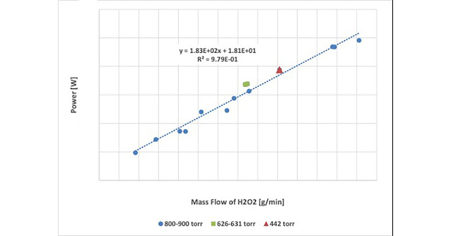
This invention correlates instantaneous applied power to mass delivery of H2O2, largely eliminating nonuniformities in the liquid source and thermal droop. This enables the Peroxidizer to provide accurate and linear delivery of chemistry without regard to vaporization temperature or process pressure.
“By applying this new process control method, the Peroxidizer can provide linear control throughout the mass flow range independent of the carrier gas flow rate and operating pressure of the process,” said RASIRC Founder and CEO Jeffrey Spiegelman. “This design integrates custom hardware, firmware and software to improve both Peroxidizer performance and tool-to-tool repeatability, helping us meet the semiconductor standards for high volume manufacturing (HVM).”
Power control is a very effective way to deliver vapor from a liquid source. Most liquid to vapor mass flow control is managed by temperature regulation of the liquid source or bath. However, bath temperature increases with increased mass flow rate causing temperature non-uniformities, localized droop, and output instabilities. As the temperature increases the vapor pressure increases on a power curve. Error increases in a highly non-linear fashion. For example, H2O2 vapor pressure change of 1°C at 90°C is 20 times larger than 1°C at 30°C, leading to 20X increased error at the higher temperature. Power control is based on the mass evaporated so the error does not increase with increasing bath temperature.
About the RASIRC Peroxidizer®
The RASIRC Peroxidizer provides a safe, reliable way to deliver high-concentration hydrogen peroxide gas into ALD, annealing, gapfill, dry surface preparation, and cleaning processes.
About RASIRC
RASIRC transforms liquids into dynamic gases that power process innovation in semiconductor and adjacent markets. By commercializing molecules for lower temperature processes, RASIRC patented technology enables the manufacture of atomic-scale oxides, nitrides, and metals. Innovative products such as Brute Peroxide, Brute Hydrazine, the Peroxidizer, and the Rainmaker Humidification Systems are being used to develop solutions for 5G, AI, IOT, and advanced automation.
What makes RASIRC a unique industry leader is our technical expertise and commitment to solving complex industry challenges for our customers. Our team of industry experts has a proven track record of beating larger competitors to market by efficiently delivering state of the art technology that reduces cost, improves quality, and dramatically improves safety. With our customers at the forefront of all we do, we continue to research, develop, and design innovative products that purify and deliver ultra-pure gas from liquids for the semiconductor and related markets. Contact RASIRC to help solve your complex problems.
P: 858-259-1220, email info@rasirc.om or visit http://www.rasirc.com
Saturday, March 5, 2022
The Emergence of Hydrazine (N2H4) in Semiconductor Applications
The Emergence of Hydrazine (N2H4)
in Semiconductor Applications
by Jeffrey
Spiegelman and Daniel Alvarez
Historically, metal-nitride
MOCVD and ALD films have been fabricated with Ammonia (NH3). However, lower thermal budgets and shrinking 3-dimensional
structures are needed for next generation semiconductor devices. These challenges have exposed limitations
with ammonia which could be overcome by replacing ammonia with hydrazine (N2H4). Purity of commercially available hydrazine has delayed its adoption. RASIRC Inc. has recently developed a new
formulation of hydrazine called BRUTE® Hydrazine which is safer and meets
purity requirements for semiconductor manufacturing. Prior to Brute Hydrazine,
the body of technical data applicable to semiconductor processing was limited
and scattered. This paper provides an
overview of the growing activity in the thin film use of Brute hydrazine as
well as early references on laboratory grade hydrazine for historical
completeness.
Increasing
Need for More Reactive Nitrogen Sources
Emerging devices
such Logic and Advanced Memory require high quality thin (5-20 Å) electrode and
barrier films. Difficult thermal budget
constraints are now being placed on well-known materials such as SiNx,
TiNx and TaNx.1-3 Deposition temperature limitations have dropped
to 350°C and below while very low resistivity (<150 micro-ohm/cm) for TiN
and TaN must still be achieved. Although
metal and nitride films grown using plasma assisted processes (PE-ALD) and
(PE-CVD) at low temperatures exhibit enhanced properties, the damage induced by
plasma on sensitive substrates is one of the common drawbacks,4,5 as
well as inability to support HAR or three-dimensional structures like
horizontal vias and deep trenches.
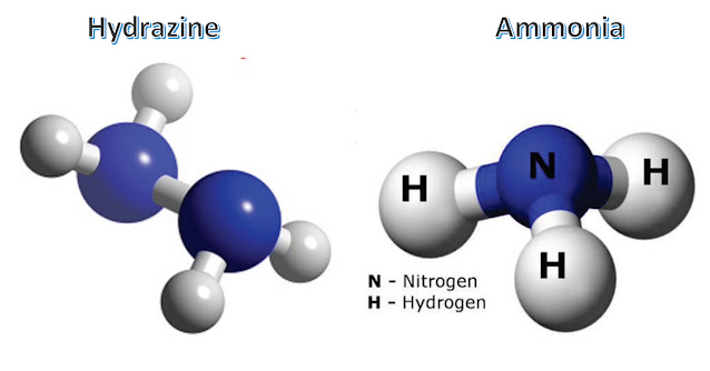
In addition to growing thin nitride films, hydrazine can also act as a reducing agent for several late transition-metals. This work is highly relevant to the use of hydrazine as a surface cleaning agent as well as a potential adder for metal ALD.7
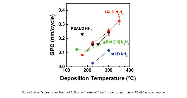
Figure 1: Low Temperature Thermal ALD growth rate
with Hydrazine comparable to PEALD with Ammonia.
The following table provides primary references for the areas of hydrazine ALD/CVD relevant to Semiconductor device applications. Additional relevant references on related films are also included.
|
Precursor and
Temperature |
Film |
Reference |
|
Al surface nitridation 200C-450C |
AlN |
Taylor
et.al. U.S. Patent 6465350, 2002 |
|
TMA MOCVD
300C-400C |
AlN |
Fujieda, S. et. al. Adv.
Func. Mat. 1996, 6(3), 127-134 |
|
TDEAA 150C-225C |
AlN |
Abdulagatov, A.I. et. al. Russian Microelectronics, 2018,
47(2), 118–130. |
|
TMA 175C-350C |
AlN |
Jung, Y.C. et. al. Materials 2020, 13, 3387; https://doi:10.3390/ma13153387 |
|
TDMAA 225C-400C |
AlN |
Ueda, S.T. et. al. Appl.
Surf. Sci. 2021, 554, 149656 |
|
BCl3 ,
350C |
BN |
Wolf, S. et. al. Appl. Surf. Sci. 2018, 439, 689–696 |
|
Surface Clean 200C |
Cu |
Hwang, S.M. et.
al. ECS Trans. 2019, 92, 265 |
|
Surface Clean 100C-300C |
Cu, Co |
Hwang, S.M. “Effect of
Surface Cleaning Efficacy on Vapor-Phase Cleaning of Cu and Co Using Anhydrous
N2H4” AVS ALD/ALE 2021 Session: Area Selective ALD AS4-1 |
|
TMG, 400C-800C |
GaN |
Fujieda, S. et.
al. Jpn. J. Appl. Phys. 1987,
26, 2067-2071 |
|
TMG, TMI, 600C-900C Theoretical |
GaN, InGaN |
Koukitu, A. et. al. phys. Stat. sol. (b), 1999,
216(1), 707-712 |
|
TMG Theoretical |
GaN |
Goddard, W. et.al. J. Phys. Chem. C 2015, 119(8) 4095–4103 |
|
[Ru(DMBD)(CO)3] 200C. Metal Deposition |
Ru |
Cwik, S. et. al. J. Vac. Soc. Sci. & Tech. A 2020, 38, 012402; https://doi.org/10.1116/1.5125109 |
|
SiH4 550C-1050C |
SiN |
Yoshioka, S. et. al. J.
Electrochem. Soc. 1967, 114, 962–964. |
|
SiH4/W hot wire 300C |
SiN |
Matsumura, H. 1989 Jpn. J. Appl. Phys. 28 2157 |
|
Si2H6,
Si3H8 350C-550C |
SiN |
Kanoh, H. et al. “Low-Temperature Chemical-Vapor-Deposition of
Silicon Nitride” Journal de Physique IV
Proceedings, 1991, 02 (C2),
pp.C2-831-C2-837. |
|
Si surface Nitridation. 300C-500C |
SiN |
Abyss, J.A.
et. al. J. AIChE 1995,
41, 2282–2291 |
|
Si2Cl6 285C |
SiN |
Edmonds, M. et. al., J. Chem. Phys. 2017, 146,
052820 ; https://doi.org/10.1063/1.4975081 |
|
Si2Cl6 320C-410C |
SiN |
Kondusamy,
A. et.
al. “Low Temperature Thermal ALD
of Silicon Nitride Utilizing a Novel High Purity Hydrazine Source”, Electrochem. Soc. AiMES 2018, Meet.
Abstr. G02-993 |
|
Si2Cl6 410C-650C |
SiN |
Le, D.N. et al “Thermal Atomic Layer Deposition
of Silicon Nitride Using Anhydrous Hydrazine and Ammonia” AVS ALD 2021, Session AF9. |
|
TBTDET 150C-250C |
TaN |
Burton, B.B., et. al. J. Electrochem. Soc. 2008,
155, D508 |
|
TBTDET 100C-300C |
TaN |
Wolf, S. et.al. Appl.
Surf. Science, 2018, 462,
1029-1035 |
|
TDMAT 200C |
TiN |
Wierda, D.A. et. al. Electrochemical and Solid-State
Letters, 1999, 2 (12) 613-615 |
|
TiCl4 200C-350C |
TiN |
Abdulagatov,
A.I. Ph.D. Thesis, Univ. of Colorado, 2012, UMI No.
3549153 |
|
TiCl4
300C-400C |
TiN |
Wolf, S. et.al. Appl.
Surf. Science, 2018, 462,
1029-1035 |
|
TiCl4 300C-400C |
TiN |
Kuo, C.H. et. al. “Low Resistivity Titanium Nitride Thin Film Fabricated by Atomic Layer
Deposition on Silicon” AVS ALD 2021, Session
AM5-9. |
|
TiCl4
250C-400C |
TiN |
Alvarez, D. et. al. “Comparative Study of Titanium Nitride ALD
using High Purity Hydrazine vs Ammonia” Electrochem.
Soc. 2020 Meet. Abstr. MA2020-02 1668 |
|
BTBMW 300C |
WN |
Bernal-Ramos, K.
Ph.D.
Thesis, Univ. of Texas, Dallas, 2014, UMI No. 3668896 |
|
BTBMW 250C-350C |
WN |
Le, D.N. et.al.
“Atomic Layer Deposition of Nanometer Thick Tungsten Nitride Using Anhydrous
Hydrazine for Potential X-Ray Optics Application” AVS ALD/ALE 2021
Session: AF10-15 |
Discussion on Specific Films
Titanium
Nitride (TiN) is a critical film in semiconductor
manufacturing. Commonly TiN is utilized as an electrode material as well as a
low resistivity barrier layer. Early CVD
work by Wierda demonstrated low temperature (50C-250C) TiN CVD by hydrazine and
TDMAT. Optimal results were obtained
when 1.9% hydrazine was combined with ammonia.
This may be attributed to a different mechanistic pathway or ammonia
dilution of oxygen containing contaminants.
Wolf later demonstrated low temperature (300C) TiN ALD with the use of
TiCl4. This result was then optimized by Kuo in the same lab, where
resistivities well below 180 micro-ohm/cm were achieved by reducing oxygen
contamination in the film through improved hydrazine purity. A comparative
study of Hydrazine vs Ammonia for TiCl4 was reported by Taiyo Nippon
Sanso, where the two nitrogen sources showed highly disparate growth rates and
film properties. Hydrazine demonstrated
viability at the 250C-400C range for low temperature semiconductor
applications.
Silicon
Nitride (SiN) is a widely used material in
semiconductor devices. SiN is commonly used as an etch stop, a dielectric
layer, an encapsulation layer, and as a barrier layer on organic devices. As early as 1967, hydrazine and Silane CVD
was demonstrated at 550C. This work was
then followed-up by Kanoh with higher silanes in the 350C-550C range. In a very interesting approach, Abyss
demonstrated Si surface nitridation with hydrazine at temperatures as low as
300C. More recently, Edmonds cleverly
used hydrazine/hexachlorodisilane ALD to place a thin SiN passivation layer on
SiGe at 285C. Extensive studies have
been carried out by the Kim group at UT Dallas in the range of 320C-650C. Below 400C, thermal ALD leads to films with
good composition, but unfavorable low density and high wet etch rates. This can be overcome with addition of Argon
plasma densification. At 480C and above,
thermal ALD films are grown with high density, low wet etch rates, and reduced
hydrogen incorporation. When compared to
ammonia grown films in the same temperature range, the hydrazine ALD films are
superior up to temperatures >600C where films properties become more
similar.
Gallium
Nitride and Indium Gallium Nitride (GaN, InGaN) grown
with hydrazine have had few publications in the last 20 years despite interest
in reduction of ammonia usage and poor indium incorporation. These films are
central in LEDs and emerging power devices.
Fujieda demonstrated that overall chemical consumption can be greatly
reduced with hydrazine vs ammonia for GaN deposition in the 400C-800C
range. Koukitu followed this up with a theoretical
thermodynamic study showing how the use of hydrazine can reduce deposition
temperature and stabilize composition for GaN and InGaN films. In 2015, Goddard elucidated the likely
mechanisms for hydrazine vs ammonia is GaN deposition.
Though little
has been published for GaN/InGaN deposition with hydrazine, viability for III/V
materials can be inferred from work published for AlN ALD with hydrazine. Fujieda reported MOCVD with trimethyl
aluminum (TMA) in the 300C-400C range.
More recently Jung reported ALD with TMA as low as 175C and compared to
ammonia in the 175C-350C range. Abdulagatov made use of the nitride-based
ligands with TDEAA/hydrazine ALD in the 150C-250C range. In a similar approach using TDMAA, Ueda has
reported the deposition of crystalline AlN films as low as 350C with thermal
ALD. With the addition of Argon plasma densification,
crystalline films can be obtained as low as 225C, where crystallinity in AlN
was optimized at 400C.
Copper,
Cobalt and Ruthenium can be reduced in situ by Hydrazine. Furst provided a detailed review on hydrazine
as a reducing agent for organic compounds.8 Recently Hwang reported
an extension of this reactivity to Cu surfaces.
Gas phase reduction of Cu oxides to Cu metal with hydrazine at moderate
temperatures (100C-300C) was reported.
Here, hydrazine is introduced in short pulses, analogous to an ALD
reaction. A similar report for Cobalt has also been presented by Hwang. Cwik working in the Winter group has recently
released data showing the ability to grow Ru metal using hydrazine as a
reducing agent in Ru ALD at 200C. Here
hydrazine was found to be advantageous over substituted hydrazine derivatives.
Conclusion
Hydrazine is
emerging as a replacement for ammonia in low temperature applications. Recent
examples of different production-worthy nitrides have been reported for both
ALD and MOCVD films. These positive
reports have led to an increasing level of interest within the scientific community
looking for solutions to new device structures and increased density.
Contact
the Author
The author is
available for additional technical discussion. Contact
RASIRC to schedule an appointment.
References
1. Burton BB, Lavoie AR, George SM (2008) Tantalum nitride atomic layer deposition using (tert-Butylimido) tris(diethylamido)tantalum and Hydrazine. J Electrochem Soc 155, D508
2. Alvarez, D.; Spiegelman, J.; Andachi, K.; Holmes, R.; Raynor, M.; and Shimizu, H. Enabling Low Temperature Metal Nitride ALD Using Ultra-High Purity Hydrazine: ET/ID: Enabling Technologies and Innovative Devices. 2017 28th Annu. SEMI Adv. Semicond. Manuf. Conf., Saratoga Spring, NY, USA, 2017, 426–430.
3. Hwang, S.M.; Kim, H.S.; Le, D.N.; Ravichandran, A.V.; Sahota, A.; Lee. J.; Jung, Y.C.; Kim, S.J.; Ahn, J.; Hwang, B.K.; Lee, L.; Zhou, X.; and Kim, J. Plasma-Enhanced Atomic Layer Deposition of Nanometer-Thick SiNx Films Using Trichlorodisilane for Etch-Resistant Coating. ACS Appl. Nano Mater. 2021, 4, 2558–2564. https://doi.org/10.1021/acsanm.0c03203.
4. Kim, H.; Oh, I.-K.; Review of Plasma-Enhanced Atomic Layer Deposition: Technical Enabler of Nanoscale Device Fabrication. Jpn. J. Appl. Phys. 2014, 53, 03DA01. https://doi.org/10.7567/JJAP.53.03DA01.
5. Mussroot, J. et.al. Microelectronic Engineering 86 (2009) 72-77. http://dx.doi.org/10.1016/j.mee.2008.09.036
6. Ravinder Kour et al 2020 ECS J. Solid State Sci. Technol. 9, 015011
7. Hwang, S. M.; Peña, L. F.; Tan, K.; Kim, H. S.; Kondusamy, A. L. N.; Qin, Z.; Jung, Y. C.; Veyan, J.-F.; Alvarez, D.; Spiegelman, J.; et al. Vapor-Phase Surface Cleaning of Electroplated Cu Films Using Anhydrous N2H4. ECS Trans. 2019, 92, 265–271.
8. Furst, A. et. al. Chem. Rev. 1965, 65, 51–68.
Subscribe to:
Posts (Atom)