Saturday, January 25, 2020

Chlorine-free titanium ALD precursor for leading edge semiconductor applications


Strem´s TDMAT ALD precursor as an attractive alternative to TiCl4

Atomic layer deposition (ALD) of titanium-based compounds has been a crucial process step in the modern semiconductor industry. Titanium nitride (TiN), due to its high electrical conductivity, has been in use as an inorganic anti-reflective coating for lithography, hard-mask for low-κ patterning, transistor gate electrodes, and diffusion barrier for tungsten contacts and Cu interconnects. Intel, in its 10nm, 3rd generation FinFET based technology node, employs a conformal Ti layer to wrap around source/drain diffusion regions to lower the spreading resistance (Link). Apple’s A11 bionic processor chip based on TSMC’s 10nm technology and Samsung’s Exynos 8895 processor chip based on its 10nm technology also incorporates Ti-based liners for tungsten contacts (Link). Globalfoundries and IBM Research investigated cobalt as a replacement of tungsten in the contacts for advanced semiconductor chips, and this process also incorporated a TiN barrier and a Ti liner (Link). TiN electrodes have also been promising for ferroelectric memory applications.


Figure 1:  Cross-section, perpendicular to the fin direction, TEM images on the 6T-SRAM area for (a) A11 and (b) Exynos8895. Images (c) and (d) are corresponding EDS mappings of (a) and (b), respectively. (Picture credit: MSSCORPS CO., LTD.)


Titanium dioxide (TiO2) is also an attractive candidate for several thin-film applications, such as high-k material for electronic devices, anti-reflection optical coatings, biocompatible coatings, photocatalysis, and solar cells. Besides, TiO2 is also a constituent of several crucial multi-metal oxide systems, such as strontium titanates (STOs), barium strontium titanates (BSTs), and lead zirconium titanates (PZTs), for dielectric and ferroelectric applications.

The TiCl4 precursor has been widely used to deposit Ti-based thin-films. However, due to severe Cl contamination, low growth per cycle, the corrosive nature of the reaction by-product (mainly HCl), high process temperature, and lower reactivity of TiCl4, the industry switch over to metal-organic precursors is swiftly gaining traction.

Strem Chemicals, Inc., a leading fine chemicals supplier, headquartered in Newburyport, Massachusetts, USA, boasts a vast variety of metal-organic precursors for depositing superior Ti-based thin-films in semiconductor as well as non-semiconductor applications. TDMAT [tetrakis(dimethylamino)titanium(IV)] (Product Catalog Number: 93-2240, CAS Number: 3275-24-9) is one of the most preferred high-purity metal-organic precursors in Strem’s chemical offering. Highly volatile and reactive TDMAT offers adequate vapor pressure even at room temperature and enables low temperature (< 140°C) deposition of high-quality Ti-based thin-films.


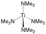
Figure 2: TDMAT molecule
 
Since 1964, Strem Chemicals, Inc. has been serving its clients from academic, industrial and government research and development laboratories as well as commercial scale businesses in the pharmaceutical, microelectronic and chemical/petrochemical industries. Strem also provides custom synthesis (including high-pressure synthesis) and current good manufacturing practice (cGMP) services. With ISO 9001 certification for Quality Management System (QMS) standard and documentation, most of Strem’s products are of reliable high purity, typically 99%, with some at 99.9999% metals purity. Strem utilizes a comprehensive range of analytical techniques tailored to each product to ensure quality because the researchers typically rely on the supplier's quality procedures and documentation, which may be detrimental to a great research idea if poorly conducted. All of Strem's catalogs, since inception, have listed “Color and Form” for every product as primary indicators of quality.

More than fifty years of experience in manufacturing inorganic and organometallic chemicals has enabled Stem to expand its product offering of MOCVD, CVD, and ALD precursors. They are continually adding new products for this dynamic and exciting field. Strem’s product range includes:


Product mentioned in this blog:
93-2240: Tetrakis(dimethylamino)titanium(IV), 99% TDMAT (3275-24-9)

Related Product Lines & Resources:
CVD & ALD Precursors
MOCVD, CVD & ALD Precursors Booklet
See full Material Science product line
---
Promotional Blog for Strem Chemicals, Inc.
Researched, produced & written by BALD Engineering AB, Stockholm, 2020-01-25
Abhishekkumar Thakur, Jonas Sundqvist
www.baldengineering.com


Friday, January 24, 2020

Program release - EFDS ALD for Industry 2020 in Freiburg, Germany (March 31-April 1)

A topical workshop with a focus on industrialization and commercialization of ALD for current and emerging markets

Atomic Layer Deposition (ALD) is used to deposit ultraconformal thin films with sub-nm film thickness control. The method is unique in the sense that it employs sequential self-limiting surface reactions for growth in the monolayer thickness regime. Today, ALD is a critical technology in leading-edge semiconductor technology, and the field of application in other industries is increasing rapidly. According to the market estimates, the equipment market alone is currently at an annual revenue of US$ 1.8-1.9 billion (2018), and it is expected to double in the next 4-5 years. In a European context, ALD was invented independently twice in Europe (Russia & Finland), and since the last 15 years, Germany has grown to become one of the strongest European markets for ALD in R&D, chemicals, equipment, and end-users.
Keynote: Prof. Henrik Pedersen, Linköping University
Tutorials by : Bochum University, Lund University, Uppsala University, Oxford Instruments, TECHCET / Fraunhofer IKTS 
Presentations by: Air Liquide, BASF, CEA Leti, Encapsulix, Picosun, Veeco, Sentech, Beneq, Fraunhofer IPMS-CNT, Positive Coating, ATLANT 3D Nanosystems, Fraunhofer FMD 
This year we will organize the 4th Workshop „ALD For Industry“ in South Germany (Freiburg), much closer to the other ALD hubs in continental Europe in France, The Netherlands, Belgium, Italy, and Switzerland. ALD for Industry provides the opportunity to get in contact with industrial and academic partners to learn more about the fundamentals of ALD technology and to get informed about recent progress in the field. The Event will focus on the current markets for ALD and addresses the applications in the Semiconductor industry, MEMS & Sensors, Battery Technology, Medical, Display, Lightning, Barriers, and Photovoltaics.
Program and Information: LINK

ALD Industrial Exhibition (more in the pipeline):


Russian researchers obtain atomically thin molybdenum disulfide (2D) films on large-area substrates by ALD

[Press release: LINK] Researchers from the Moscow Institute of Physics and Technology have managed to grow atomically thin films of molybdenum disulfide spanning up to several tens of square centimeters. It was demonstrated that the material’s structure can be modified by varying the synthesis temperature. The films, which are of interest to electronics and optoelectronics, were obtained at 900-1,000 degrees Celsius. The findings were published in the journal ACS Applied Nano Materials.


An atomic layer deposition reactor from Picosun used for obtaining ultrathin molybdenum oxide films, which were subsequently sulfurized to 2D molybdenum disulfide. Image courtesy of the Atomic Layer Deposition Lab, MIPT

Two-dimensional materials are attracting considerable interest due to their unique properties stemming from their structure and quantum mechanical restrictions. The family of 2D materials includes metals, semimetals, semiconductors, and insulators. Graphene, which is perhaps the most famous 2D material, is a monolayer of carbon atoms. It has the highest charge-carrier mobility recorded to date. However, graphene has no band gap under standard conditions, and that limits its applications.


Scaled perovskite solar modules pass three critical stability tests

[Press release: LINK] Eindhoven (Netherlands), Genk (Belgium) January 23, 2020 – Solliance partners TNO, imec and the Eindhoven University of Technology, demonstrated encapsulated perovskite solar modules fabricated using industrial processes that withstand three established lifetime tests, i.e. the light soak test, the damp-heat test and the thermal cycling test. It is for the first time this milestone is passed with scaled perovskite solar modules prepared by research organizations.


Perovskite solar cells and modules, are nowadays widely acknowledged for their high efficiency values of up to 25.2% for the current latest record lab solar cell. Perovskite solar cells and modules combine high efficiency with low cost processability and are based on low cost and abundant materials. Furthermore, perovskite solar modules can be either rigid or flexible as well as opaque or semi-transparent. This allows a wide range of applications.

One can think of perovskite modules integrated in windows, roof tiles, facades, roads, noise barriers, car roofs – it is envisioned that these perovskite solar modules can be seamlessly integrated in an aesthetical manner with high social acceptance on any surface which receives light. Additionally, tandem solar modules consisting of a semitransparent perovskite module stacked on top of a conventional CIGS or silicon solar module can boost the overall efficiency to new record values.

Monday, January 20, 2020

Forge Nano Webinar - Lab Scale ALD on powders with PROMETHEUS

Forge Nano has started to provide free ALD Webinars given live as well as playback thru their website: LINK

FREE ALD Webinar - Lab Scale ALD on powders with PROMETHEUS
  • Join the ALD experts at Forge Nano for a free webinar on Jan. 30th @ 10:00am MST.
  • Join us as our experts demonstrate our Lab-Scale ALD tool- PROMETHEUS.
  • Get an up-close and personal look at the features and functionality of PROMETHEUS.


PROMETHEUS is a Lab-Scale, Particle ALD research tool like no other. Featuring a simple to use interface, ergonomic and intuitive design, and various reactor sizes and configurations.

Previous Webinar - ALD Basics – ALD on powders (LINK)


Friday, January 17, 2020

The 5th International Conference on ALD Applications & 1st Asian ALD Conference (2020 China ALD

Following the successes of the previous four International Conferences on ALD Applications and China ALD Conferences since 2010, the 5th International Conference on ALD Applications & 1st Asian ALD Conference (2020 China ALD) will be a three-day meeting, dedicated to the fundamentals and applications of Atomic Layer Deposition (ALD) technology in various fields. It will be held in Wuhan, China, from October 12 to 14, 2020. This conference will feature plenary sessions, oral sessions, poster sessions and industrial exhibitions.

The ALD technique has been widely used and explored in numerous fields such as microelectronics, photoelectronics, optical coating, functional nanomaterials, MEMS/NEMS, energy storage, biotechnology, catalysis technology, and etc.

Conference web: http://www.c-ald.com/

Program Chair

Rong Chen (Huazhong University of Science and Technology, China)

Program Co-Chairs

Chang Liu (Wuhan University, China)

Soo-Hyun Kim (Yeungnam University, South Korea)