Thursday, November 21, 2019

PEALD processes employing Strem supplied TDMASn precursor presented by diverse groups of researchers

We offer prepackaged precursors in ALD Cylinders!


Atomic layer deposition (ALD) using Tin (Sn) based compounds have been widespread in applications, such as sensors, Li-ion batteries, catalysts, photovoltaics. Recently, researchers have reported state-of-the-art applications like 3D thin-film solid-state batteries (by Pearse et. al.) and efficient perovskite solar cells (by Guan et. al. and Sun et. al.). Many of these applications feature layers that are susceptible to degradation at elevated temperatures. It’s mandatory to deposit SnO2 below 200°C for applications such as perovskite and silicon heterojunction solar cells. Alternatively, plasma-enhanced atomic layer deposition (PEALD) with Strem Chemicals’ highly reactive metalorganic precursor, tetrakis(dimethylamino)tin (TDMASn), with a decomposition temperature range of 250–300°C, also enables low deposition temperatures. 


Figure 1. 50-1815 Structure


Strem Chemicals offers TDMASn [Sn[N(CH3)2]4] (catalog number 50-1815) precursor, which has been widely accepted in the PEALD community worldwide for the deposition of tin-based compounds. The colorless to pale yellow liquid phase precursor with a density of 1.169 at 20°C and vapor pressure of 15 Torr is sold pre-packed, in an ALD cylinder by Strem Chemicals (98-4050).
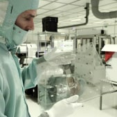


The following are some of the examples of PEALD processes employing Strem supplied TDMASn precursor presented by diverse groups of researchers. 

Hoffmann et. al. report the preparation of transparent conductive gas permeation barriers based on thin films of tin oxide (SnOx) grown by spatial atomic layer deposition (ALD) at atmospheric pressure. They present a comparative study using tetrakis(dimethylamino)tin(IV) and various oxidants (atmospheric pressure oxygen plasma, ozone, and water) at process temperatures in the range of 80–165°C. (Link)


Recent reports by researchers from the Eindhoven University of Technology in collaboration with the Netherlands Organisation for Applied Scientific Research (TNO), present an extensive characterization of plasma-assisted atomic-layer-deposited SnO2 layers. They aim at identifying key material properties of SnO2 to serve as an efficient electron transport layer in perovskite solar cells. The SnO2 thin films were deposited at substrate temperatures of 50, 100, 150, and 200°C on Czochralski polished c-Si (100) wafers and indium tin oxide (ITO) glass substrates in an Oxford Instruments OpAL ALD reactor using tetrakis(dimethylamino)tin (TDMASn) (99% purity, Strem Inc.) as the tin precursor and radio-frequency (RF) inductively coupled oxygen plasma as the co-reactant. (Link)


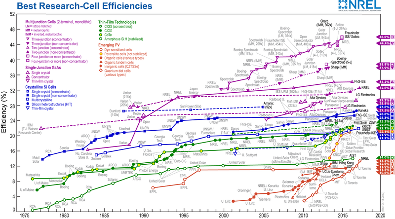
Figure 3: Perovskite solar cells are one of the most promising emerging cell technologies with fast recent improvement in cell efficiency shown above red/yellow circles reaching >22% cell efficiency (From Wikimedia Commons, the free media repository).


An American researcher from University of Maryland, U.S. Naval Research Laboratory and Sandia National Lab, has reported the experimental realization of fully conformal 3D thin-film solid-state batteries (3D TSSBs) incorporating a SnNx anode (deposited at 200°C using TDMASn and an N2 plasma), demonstrating the simultaneous power-and-energy benefits of 3D structuring. All active battery components—electrodes, solid electrolyte, and current collectors—were deposited by atomic layer deposition (ALD) onto standard CMOS processable silicon wafers. The wafers were microfabricated to form arrays of deep pores with aspect ratios up to approximately 10. Their work shows that the exceptional conformality of ALD, combined with conventional semiconductor fabrication methods, provides an avenue for the successful realization of long-sought 3D TSSBs which provide power performance scaling in regimes inaccessible to planar form factor cells. (Link)
Since 1964, Strem Chemicals, Inc. has been serving its clients from academic, industrial and government research and development laboratories as well as commercial scale businesses in the pharmaceutical, microelectronic and chemical/petrochemical industries. Strem (Headquarters: Newburyport, Massachusetts, USA) is a high purity specialty chemicals manufacturer and supplier. Strem also provides custom synthesis (including high-pressure synthesis) and current good manufacturing practice (cGMP) services. Strem’s products are of high purity, typically 99%, with some at 99.9999% metals purity. 


More than fifty years of experience in manufacturing inorganic and organometallic chemicals has enabled Strem to expand its product offering of MOCVD, CVD, and ALD precursors. They’re continually adding new products for this dynamic and exciting field. Strem’s product range includes:


·         Metal alkyls
·         Metal alkylamides
·         Metal amidinates
·         Metal alkoxides
·         Metal β-diketonates
·         Metal cyclopentadienyls
·         Metal halides
·         Volatile organometallics
·         Volatile metal carbonyls
·         Electronic grade chemicals

Additional Resources:


----------
Promotional blog written and researched by Abhishekkumar Thakur and Jonas Sundqvist, BALD Engineering AB


Monday, November 18, 2019

2020 CMC Conference & Call For Papers

San Diego, CA, November 12: The Critical Materials Council (CMC) of semiconductor fabricators and TECHCET announce the CMC Conference Call For Papers (CFP) for the event happening April 23-24 in Hillsboro, Oregon. The 2020 CMC Conference (https://cmcfabs.org/cmc-conference-2020/) will explore actionable technical and supply-chain trends related to critical materials for global semiconductor fabs. Keynote address for this 5th CMC Conference will be:

"Critical Materials Pushing the Limits for Semiconductor Manufacturing"

Bruce Tufts, Vice President of Technology and Director of Fab Materials Org., Intel Corp. 

The conference committee is soliciting presentations on best practices of sourcing direct and indirect manufacturing materials for pilot lines and for high-volume manufacturing (HVM). Three sessions will cover the following themes:

I. Global Value-chain Issues of Economics and Regulations,

II. Immediate Challenges of Materials & Manufacturing, and

III. Emerging Materials in R&D and Pilot Fabrication.


CMC member companies will be attending the public CMC Conference, which follows the annual members-only CMC meeting to be sponsored by Intel and held April 21-22. Conference attendees will include industry experts handling supply-chains, business-development, R&D, and product management, as well as academics and analysts. Business drives our world, but technology enables the profitable business of manufacturing new devices in IC fabs, and new devices need new materials.

To submit a paper for consideration, please send a 1-page abstract focusing on critical materials supply dynamics by January 15, 2020 to cmcinfo@techcet.com


----------
For more information on CMCFabs or CMC Associate Memberships, please contact Diane Scott at dscott@techcet.com. For information on sponsoring the CMC Conference please contact Yvonne Brown at ybrown@techcet.com, +1-480-382-8336 x1.

CMC Fab members include:


USITC may close Hanwha’s Patent Infringement Case indefinitely

According to TaiyangNews (LINK), South Korea’s Hanwha Q Cells patent infringement case against solar PV manufacturers JinkoSolar, REC Group and LONGi Solar apparently has hit a bump as JinkoSolar claims that in the next two weeks, the Administrative Law Judge (ALJ) in the US International Trade Commission (USITC) will put a stay on the hearing indefinitely.

The dispute is regarding Hanwa Q Cells patent on employing a surface-passivating dielectric double laye, either Al2O3 or SiN deposited by ALD or PECVD.


US9893215B2 (LINK): Method for manufacturing a solar cell with a surface-passivating dielectric double layer, and corresponding solar cell - A solar cell with a dielectric double layer and also a method for the manufacture thereof are described. A first dielectric layer (3), which contains aluminum oxide or consists of aluminum oxide, and a second, hydrogen-containing dielectric layer (5) are produced by means of atomic layer deposition, allowing very good passivation of the surface of solar cells to be achieved.

Intel to Reclaim Number One Semiconductor Supplier Ranking in 2019

According to IC Insights, Intel is to reclaim the number one semiconductor supplier ranking in 2019 from Samsung due to the downturn in Memory (DRAM and NAND). The top 3 memory suppliers (Samsung, SK Hynix, and Micron) are according to IC Insights forecast to register ≥29% year-over-year declines in 2018 with SK Hynix expected to decline the most by a 38% down in sales 2019.


The expected top 15 semiconductor (IC and O-S-D—optoelectronic, sensor, and discrete) sales ranking for 2019 is shown above.  It includes six suppliers headquartered in the U.S., three in Europe, two each in South Korea, Japan, and Taiwan.

Source: IC Insights (LINK)

Sunday, November 17, 2019

Holst Centre showcase spatial atomic layer deposition (sALD) for thin-film transistor (TFT) backplane

Researchers from Holst Centre have become the first to use spatial atomic layer deposition (sALD) to create both the semiconductor and dielectric layer in a thin-film transistor (TFT) backplane. Using a low-temperature, large-area process for the backplane, the team created a 200 ppi QVGA display demonstrator. The process allows TFTs to be produced on cheaper, transparent plastic foils, significantly reducing the cost of flexible electronics applications such as displays and image sensors. To showcase the technology, Holst Centre has produced a display demonstrator using a backplane of top-gated self-aligned TFTs on a PEN foil. The display is being presented at the International Display Workshop (IDW) in Sapporo, Japan from November 27-29.

image

The backplane was produced at temperatures below 200 °C, achieving mobilities of 8 cm2/Vs in transistors with channel lengths down to 1 μm. It was then combined with an OLED frontplane to create a 200 ppi QVGA display.


The demonstrator was produced using sALD equipment initially developed by Holst Centre and which is currently being commercialized by the start-up SALDtech. Spun out from Holst Centre in 2018, SALDtech offers the only sALD tools for Gen 1 (32 x 25 cm) substrate size flat-panel displays currently available. Earlier this year, it received a second round of investment to develop and build production equipment that could be integrated into the production lines of next-generation flexible OLED displays for mobile phones, tablets, TVs and more.


“We are already delivering TFT performance with sALD that is comparable with the best sputtered devices. And through additional optimization of processes and materials, there is considerable room for further improvements. At the same time, we are looking at producing all TFT layers with sALD to further simplify and reduce the cost of high-volume flexible TFT manufacturing,” says Ilias Katsouras, Senior Scientist at Holst Centre.

Many flat-panel displays today use the semiconductor indium gallium zinc oxide (IGZO) in the TFT backplane. IGZO is usually deposited via sputtering and requires a high-temperature anneal procedure to ensure performance. This high-temperature step necessitates substrates with high melting points, which are typically more expensive.


Developed by Holst Centre, large-area sALD is an atmospheric-pressure technique that allows ultra-thin layers of materials to be deposited quickly with high compositional control and excellent thickness uniformity. The technique has previously been used to produce high-quality individual layers of materials for solid-state batteries and TFT backplanes. Now, for the first time, Holst Centre has used sALD to deposit both the IGZO semiconductor layer and the aluminum dielectric-oxide dielectric layer in an integrated TFT process onto a low-cost, transparent plastic foil.

Using a single technique to produce multiple layers of material offers flexible TFT manufacturers the possibility of improving both production throughput and the interface between layers, which in turn increases device performance.

AlixLabs receives Vinnova grant for "Innovative startups"

93 Swedish startup companies with innovative business ideas share 28 million SEK from Vinnova. The companies receive funding to develop new solutions that can contribute to sustainable development and increased competitiveness.

The companies receive a grant of up to SEK 300,000 for developing prototypes or developing their business model. "The support enables young companies with risky projects to try their ideas and get some way to find an investor, customer or partner," says Emelie Falk, responsible for the announcement at Vinnova. Some of the startup companies that receive funding:

Some of the startup companies that receive funding:

Aquammodate AB, A new filter technique for purifying drinking water, based on natural materials with high purity and low energy consumption. 
 
HIPOR Materials AB, Reflective ceramics for space applications, which combines high insulation with high solar reflectance.

Alixlabs AB, Atomic Layer Etching for sub 10 nm semiconductor manufacturing - Proof of Concept

AlixLabs

AlixLabs logo


Fundamental to the entire IT explosion is the miniaturization that enabled an explosive increase in functionality with a reduced cost and power consumption. Moore's law describes the speed of this miniaturization in a way that has been valid since the mid sixties. However, we are now approaching a limit for the development with resolutions on individual atoms, where 10 nm corresponds to about 20 atoms.

AlixLabs has found and patented a phenomenon that makes it possible in a much simpler and cheaper way to manufacture semiconductors sub 10 nm. Our method can be said to use similar physical problems that other methods try to circumvent.

AlixLabs website

Friday, November 15, 2019

Save The Date! ALD & ALE 2020 Ghent, Belgium, June 28 and July 1, 2020

Save The Date! ALD & ALE 2020 will be held in Ghent, Belgium, between June 28 and July 1, 2020. Call for abstracts have already been opened with submission deadline on February 3, 2020.

LINK : https://ald2020.avs.org/abstract-submission/


Plasma ALD – A discussion of mechanisms – Commemorating the career of John Coburn

New Blog post by Prof. Kessels: Commemorating the work of John Coburn, how it influenced our work at TU Eindhoven in the field of ALD, and their latest work related to the surface recombination of plasma radicals and its influence on conformality of plasma-based ALD.

AtomicLimits: Plasma ALD – A discussion of mechanisms – Commemorating the career of John Coburn (LINK)