Thursday, June 20, 2019

Technical program for AVS ALD2019 and ALE2019 in Bellevue, Washington USA


Technical Program


Key Deadlines:
Hotel Reservation Deadline: June 27, 2019
JVST Special Issue Deadline: November 1, 2019

Hotel Deadline is June 27


The AVS 19th International Conference on Atomic Layer Deposition (ALD 2019) featuring the 6th International Atomic Layer Etching Workshop (ALE 2019) will be a three-day meeting dedicated to the science and technology of atomic layer controlled deposition of thin films and now topics related to atomic layer etching. The conference will take place Sunday, July 21-Wednesday, July 24, 2019, at the Hyatt Regency Bellevue in Bellevue, Washington (East Seattle). The meeting will be preceded (Sunday, July 21) by one day of tutorials and a welcome reception. Sessions will take place (Monday-Wednesday, July 22-24) along with an industry tradeshow. All presentations will be audio-recorded and provided to attendees following the conference (posters will be included as PDFs). Anticipated attendance is 800+.


Download the ALD-ALE Mobile App
Logging into the app allows you to access messaging, enable the synchronization of notes, favorites, and scheduled items between devices and the online scheduler. Click Here for Download Details 


Plenary Speaker
·    Jeff Elam (Argonne National Lab, USA)
·    Eric Joseph (IBM, USA)

ALD Invited Speakers
·    Silvia Armini (IMEC, Belgium)
·    Ageeth Bol (Eindhoven Univ. of Technology, Netherlands)
·    Jolien Dendooven (Ghent Univ., Belgium)
·    Eric Dickey (Lotus Applied Technology, USA)
·    John Ekerdt (Univ.of Texas, Austin, USA)
·    Fabio Grillo (ETH Zurich, Switzerland)
·    Hyeongtag Jeon (Hanyang Univ., South Korea)
·    Jessica Kachian (Intel, USA)
·    Rajesh Krishnamurthy (TechInsights/Chipworks, Canada)
·    Alex Martinson (Argonne National Lab, USA)
·    Niloy Mukherjee (Eugenus, Inc., USA)
·    Jin-Seong Park (Hanyang Univ., South Korea)
·    Henrik Pedersen (Linkoping Univ., Sweden)
·    Madhukar Rao (Versum Materials, USA)
·    Dina Triyoso (Tokyo Electron, USA)
·    Ginger Wheeler (U.S. Naval Research Lab, USA)
ALE Invited Speakers
·    Tomoko Ito (Osaka Univ., Japan)
·    Sabbir A. Khan (Niels Bohr Institute, Univ. of Copenhagen, Denmark)
·    Nobuyuki Kuboi (Sony Semiconductor Solutions Corp., Japan)
·    Xu Li (Univ. of Glasgow, UK)
·    Alfredo Mameli (TNO-Holst Centre, The Netherlands)
·    Angelique Raley (TEL Technology Center, America, USA)
·    Kazunori Shinoda (Hitachi Ltd, Japan)
·    Samantha Tan (Lam Research, USA)

Tutorial Speakers
·    Area-selective ALD for Semiconductor Manufacturing, Stacey Bent (Stanford Univ., USA)
·    ALD for Battery Applications, Andy Sun (Western Univ., Canada)
·    ALD for Catalysis, Rong Chen (Huazhong Univ. of Science and Technology, China)
·    ALD for Photovoltaics, Bart Macco (Eindhoven Univ. of Technology, Netherlands)
·    Plasma Based ALE, Thorsten Lill, (Lam Research, USA)
·    Thermal Based ALE, Steve George (Univ. of Colorado at Boulder, USA)


ALD Program Chairs

Program Chair:
Sumit Agarwal
(Colorado School of Mines, USA)

Program Co-Chair:
Dennis Hausmann
(Lam Research, USA)
ALE Program Chairs

Program Chair:
Craig Huffman
(Micron Technology, USA)

Program Co-Chair:
Gottlieb Oehrlein
(University of Maryland, USA)

Wednesday, June 19, 2019

TechInsights’ Logic, NAND, DRAM and Emerging Memory Process Roadmaps are here

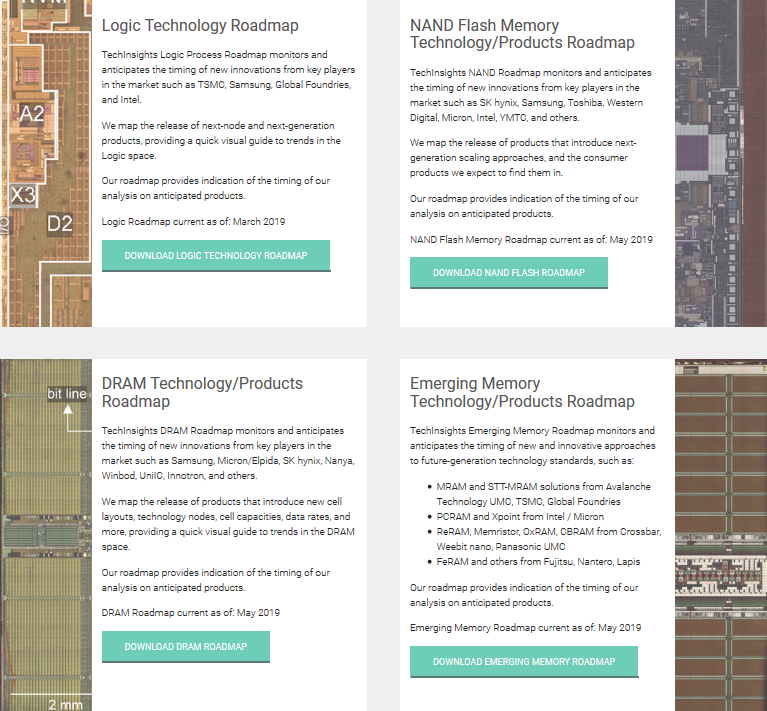
TechInsights’ Logic Process Roadmap offers an assessment and the anticipatory timing of new innovations from key players within the Logic space including: TSMC, Global Foundries, Intel & others. Download the roadmap here

TechInsights’ technology roadmaps show you the innovations we are monitoring

For over 30 years, TechInsights has been reverse engineering semiconductors and advanced technology products, developing the world’s largest library of technical analysis. We have built this library through two approaches: by conducting analysis in response to client requests, and by proactively analyzing disruptive or innovative technologies as they are released.

We constantly monitor the consumer electronics market to determine which manufacturers are planning to release new solutions, and when. We maintain and regularly update technology roadmaps in several different areas: Logic, NAND Flash Memory, DRAM, Emerging Memory, and Internet of Things Connectivity Systems on Chips, and more.

Updates to the roadmaps shown below are released throughout the year; check this page for updates. 

Thursday, June 13, 2019

Call for papers -Atomic Layer Deposition and Atomic Layer Etching in JVSTA

Manuscript Deadline: November 1, 2019

These 2020 Special Topic Collections are planned in collaboration with ALD 2019 and the ALE 2019 Workshop to be held in Bellevue, WA from July 21—July 24, 2019. The Special Topic Collection will feature sections dedicated to the science and technology of atomic layer controlled deposition and to the science and technology of controlled etching of thin films. While a significant number of articles will be based on material presented at ALD 2019 and the ALE 2019 Workshop, research articles on ALD and ALE but not presented at this conference are also welcome. The special topic collection will be open to all articles on the science and technology of ALD and ALE.

Authors are encouraged to use the JVST template. Online, you will have an opportunity to tell us that your paper is a part of the Special Topic Collection by choosing either the “ALD Special Topic Collection” or the “ALE Special Topic Collection.” See recent Collections: ALD 2019, ALE 2019, ALD 2018, ALE 2018


Tuesday, June 11, 2019

Swedish Nanexa’s PharmaShell® patent approved in Japan

[Nanexa AB, LINK] The Japanese Patent Office has approved Nanexa’s patent application for the drug delivery platform PharmaShell®.

Nanexa’s drug delivery system PharmaShell® is suitable for parenteral drug administration. The drug delivery system enables drug release in a well-controlled manner from a couple of weeks to really long depots of up to one year. By adjustments in the manufacturing process of PharmaShell®, the depot time can be controlled to the desired length.


The properties of PharmaShell®, with extremely high so-called drug load and the ability to control the initial release, make it unique in the market. The system enables depot preparations from simple small molecule drugs to proteins. The mentioned properties are in demand by the pharmaceutical industry to create new and more effective drugs with the possibility of limiting the side effects of the drug.

The Japanese Patent Office has approved Nanexa’s patent application on May 30, 2019. The now approved patent covers the product PharmaShell® itself and the method of its manufacture and formulation of PharmaShell® coated drugs. The approved patent has patent number JP6516729.

CEO David Westberg comments:

In January, we got the PharmaShell® patent approved in the US and I can now conclude that it has also been approved in Japan. The Japanese market is large and important for Nanexa and with an approved patent our commercial opportunities in the future will increase.

Our continuous work on patent applications begins to yield results and together with our more recently filed patent applications, I assess that we have a strong patent portfolio.

Previous News on Nanexa:

Nanexas PharmaShell® patent approved in the United States

Nanexa order a third Picosun ALD System to meet production demand for PharmaShell®

Nanexa has completed a safety laboratory for the PharmaShell® process

New method using ALD enables storage and controlled release of pharmaceutical substances in the body