Sunday, November 19, 2017

Atomic Layer Etching is entering HVM for sub 14 nm Logic

After years in R&D, several fab tool vendors last year finally began to ship systems based a next-generation technology called atomic layer etch (ALE).

ALE is is moving into 16/14nm, but it will play a big role at 10/7nm and beyond. The industry also is working on the next wave of ALE technology for advanced logic and memory production.

Used by chipmakers for years, traditional etch systems remove materials on a continuous basis in devices. Considered a next-generation etch technology, ALE selectively removes targeted materials at the atomic scale without damaging other parts of the structure. For example, ALE can be used to remove materials in a structure to form trenches with gaps on the order of 10 to 15 angstroms or 5 atoms wide. (An angstrom is 0.1nm.)

Applied Materials Centris Sym3 is one of the Applied Materials offering for ALE. It can be configured to handle plasma ALE for anisotropic etch applications, such as self-align contacts and spacer-based patterning.

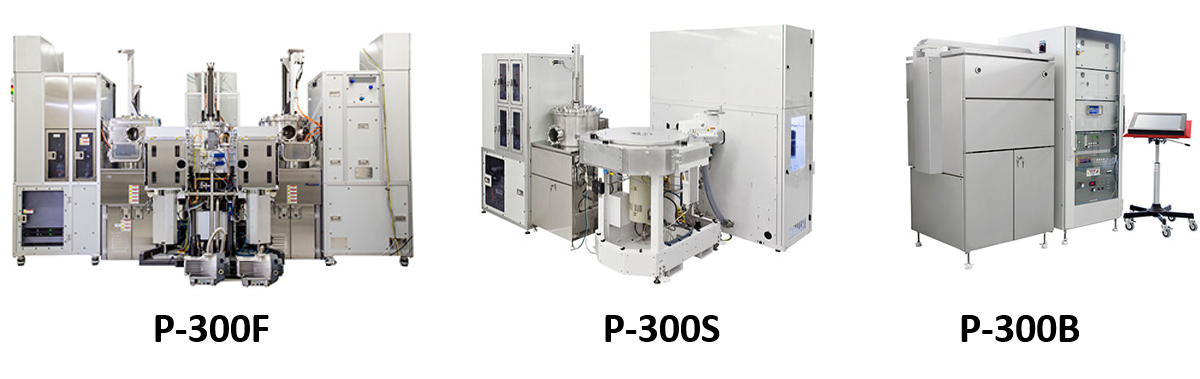
Applied Materials, Hitachi High-Technologies, Lam Research and TEL are among the suppliers of ALE tools in the market. Today, ALE represents a tiny percentage of the overall etch market. In total, the worldwide dry etch business is projected to reach $9.6 billion in 2017, up from $7.2 billion in 2016, according to Gartner.

Full article :  "What’s Next For Atomic Layer Etch?" by Mark Lapedus, Semiconductor Engineering (LINK)


Saturday, November 18, 2017

Aixtron complete sale of ALD/CVD memory product line to Eugene Technology

AIXTRON SE (FSE: AIXA), one of the world’s leading providers of deposition equipment to the semiconductor industry, announced today that the sale of AIXTRON’s ALD and CVD memory product line to Eugene Technology Inc., a wholly owned U.S. subsidiary of Eugene Technology Co., Ltd, South Korea was completed as of November 15, 2017. 

The QXP-8300 Atomic Layer Deposition (ALD) mini-batch system suitable for e.g. high-k oxide films in advanced memory applications including 3D structure devices (aixtron.com)

AIXTRON will receive c. USD 60 million for the assets being transferred and c. USD 11 million for open supplier orders for which it retains the liability to pay.

AIXTRON, Inc., the U.S. subsidiary of AIXTRON SE situated in Santa Clara, California, will continue to provide sales and support for its continuing businesses.

Arradiance and InRedox team up to offer ALD Functionalized Nanomaterials

SUDBURY, Mass., Nov. 17, 2017 —Arradiance’s formidable Atomic Layer Deposition (ALD) foundry service and InRedox’s world-class manufacturing of nanoporous anodic aluminum oxide (AAO) and nanotubular anodic titanium oxide (ATO) will provide new ALD-functionalized Nanoceramics for life sciences, nanotechnology, filtration and separation, energy generation and storage, analytical equipment and many other applications.
 

Arradiance LLC, manufacturer of the popular GEMStar family of professional, research grade Atomic Layer Deposition (ALD) systems and provider of nanofilm foundry services, today announced a partnership with InRedox LLC (Longmont, Colorado) to provide nanotechnology researchers with ALD-functionalized nanostructured materials (wafers, membranes and nanotemplates).

“InRedox’s innovative AAO / ATO wafers and templates have demonstrated utility at leading commercial, academic and government research institutions across a broad range of technology areas,” said Arradiance CEO Michael Trotter. “I am certain that the combination of Arradiance’s ALD nanofilms with InRedox’s powerful nanofabrication technology platform will spur exciting new developments,” explained Mr. Trotter.

“InRedox is excited by the potential of ALD functionalized nanoporous ceramics,” stated Dmitri Routkevitch, InRedox President and CTO, “and we look forward to working with Arradiance to continue to expand the range of nanomaterials that inspire and enable our customers in their pursuit of scientific breakthroughs or new products.”

Thermal atomic layer deposition of tungsten carbide films from WCl6 and TMA

Kyle J. Blakeney and Prof Winter from Department of Chemistry, Wayne State University just published a new exciting ALD path to tungsten carbide. WCl6 has favorable precursor characteristics and advantages over the widely used WF6, which is corrosive and toxic. In addition, fluorine tend to diffuse into dielectric layers (SiO2, SiN, high-k) and can cause reliability issues for transistor and memory devices e.g. in CMOS Logic, DRAM and NAND Flash Memory.

Films for this study were deposited in a Picosun R75-BE ALD reactor and WCl6 (99.9%, Strem)  delivered at 125 °C using the solid state booster in the reactor. You may find more details an the ALD redactors at their lab here (LINK).

Please check out the publication in JVSTA A - Open source available for all!

Free, Published Online: November 2017Accepted: October 2017
Journal of Vacuum Science & Technology A: Vacuum, Surfaces, and Films 36, 01A104 (2018); https://doi.org/10.1116/1.5002667

Nice little story on thermal #ALDep of tungsten carbide online now. TMA is definitely the most versatile ALD precursor https://t.co/65yNQpNcDl
Also nice to see the refernce No. 33 to this Blog :-)


Thursday, November 16, 2017

Beneq present ALD Throughput Revolution in More than Moore Markets

At Semicon Europa, the largest microelectronics event in Europe, 14-17, November, Munich, Germany, Beneq launched the Beneq C-Series, a new Cluster-Compatible ALD product family for high-volume manufacturing of wafers. This is the start of a throughput revolution for ALD in new More than Moore wafer processing markets. 


Beneq C2 is a cluster-compatible automated wafer ALD system for industrial processing of wafers. It is available both as a single-wafer version and as batch-processing equipment for high volume manufacturing. Beneq C2 offers a unique combination of high capacity batch processing and standard cassette-to-cassette automation. Each process module on the cluster can process up to 30 000 wafer passes per month(200 mm wafers). [beneq.com]

Please find more detailed information in the press release from Bebeq [LINK]


Wednesday, November 15, 2017

According to Amnesty Industry giants fail to tackle child labour allegations in cobalt battery supply chains

According to Amnesty International, major electronics and electric vehicle companies are still not doing enough to stop human rights abuses entering their cobalt supply chains, almost two years after an Amnesty International investigation exposed how batteries used in their products could be linked to child labour in the Democratic Republic of Congo (DRC), the organization said today.

- Survey of electronics and car companies shows major blind spots in supply chains
- Apple is the industry leader for responsible cobalt sourcing – but the bar is low
- Microsoft, Lenovo and Renault have made least progress


RATING COMPANIES
All possible actions taken None
Adequate action taken Apple - Samsung SDI
Moderate action taken Dell - HP - BMW - Tesla - LG Chem
Minimal action taken Sony -Samsung Electronics - General Motors - Volkswagen - Fiat-Chrysler - Daimler - Hunan Shanshan - Amperex Technology - Tianjin Lishen
No action taken Microsoft - Lenovo - Renault - Vodafone - Huawei - L&F - Tianjin B&M - BYD - Coslight - Shenzhan BAK - ZTE


 Movement of cobalt, from mine to global market [Source: Amnesty International]

In parallel ther are roports on price of Cobalt "Cobalt Prices to Rocket" : The Democratic Republic of Congo supplies some 60 percent of the world's cobalt- a desperately sought after metal that is the driver of our electric vehicle (EV) boom and the fodder of battery gigafactories popping up all over the world.

Buyers are under growing pressure to give up conflict cobalt and find new sources, but the timing is tough. Major automakers and battery manufacturers are scrambling to secure supplies of cobalt. Prices are soaring, and demand can only move in one direction - up.

One company in the heart of the Cobalt supply chain that do care a lot about fair and ethical sourcing of Cobalt is Umicore, please see previous report ebout their supply chain here - Umicore's pioneering approach to ethical cobalt sourcing for CVD/ALD precursors [LINK].

An industry that is not included here in the Amnesty study that has been using wast amounts of Cobalt for a long time is for instance the cemented carbide industry for hard metal tooling.

Sources:

Amnesty International - Industry giants fail to tackle child labour allegations in cobalt battery supply chains
https://www.amnesty.org/en/latest/news/2017/11/industry-giants-fail-to-tackle-child-labour-allegations-in-cobalt-battery-supply-chains/

Cobalt Prices to Rocket as Tech Giants Scramble for Supplies
https://www.prnewswire.com/news-releases/cobalt-prices-to-rocket-as-tech-giants-scramble-for-supplies-657690933.html

ALD Lab Saxony Symposium at Semicon Europa 2017

The ALD Lab Saxony just held its annual Symposium at SEMICON Europe in Munich, Germany. Prof. Bartha, Dr. Jonas Sundqvist, Dr. Martin Knaut and Dr. Christoph Hossbach have been organizing the event since 2012 in Dresden. This year about 50 persons attended the symposium.

The Intention of the Symposium is to improve visibility of the Atomic Layer Deposition technique and its capabilities and to increase the networking within the ALD community. The given talks gave an overview of current research and development topics as well as examples of ALD applications, equipment, chemical and supply chain in manufacturing. This year’s agenda combined several talks from ALD Lab Saxony members and partners from academia and industry on ALD equipment, applications, metrology as well as ALD simulations. This year the symposium was divided into two sessions: “Equipment and Applications” and “Precursors, Precursor Delivery, Metrology and Simulations”

New exciting applications in the field of MEMS were presented by Fraunhofer ISIT, ALD corrosion protection by Bosch and metal precursor sourcing and supply chain solutions by Umicore to mention a few. The complete Agenda can be found here (LINK: http://www.semiconeuropa.org/ald-lab-symposium-2017) and upon request the presentations will become available.

“Welcome”, Prof. Bartha, TU Dresden (Germany)

“ALD for Production”, Dr. Christoph Hossbach, Picosun (Finland/Germany)

“ALD equipment and precursors for high volume manufacturing”, Dr. Jonas Sundqvist, Fraunhofer IKTS (Germany) /TECHCET LLC (USA)


“ALD process monitoring with quartz crystal microbalances”, Dr. Martin Knaut, TU Dresden (Germany)

Friday, November 10, 2017

Picosun Oy shows record growth in ALD for fiscal year 2016/2017

Picosun is one of the leading suppliers of ALD thin film deposition technology for semiconductor, lightning, MEMS as well as for other industries and research. This week I had the chance to meet with Kustaa Poutiainen himself, Chairman and Chief Executive Officer of Picosun Oy. in Dresden. We had a very interesting meeting discussing recent developments in ALD Technology announced by Picosun as well as discussing the past and future outlook of ALD.   

Mr Poutiainen was in Germany to meet with customers and overseeing Picosuns activities and expansion in Germany. In the European perspective Germany is the biggest market for ALD Technology and Equipment. For those of you who do not know, Picosuns ALD equipment portfolio in detail it ranges from fully automated ALD batch and cluster systems for high volume manufacturing to smaller scale R&D and pre-pilot production tools (see below). 


A snapshot of the Picosun products - more information here.
Picosun has recently opened a branch office in Germany - Picosun Europe GmbH, headed by General Manager Dr. Christoph Hossbach, serving its growing install base of ALD equipment on the German market, both at leading research institutes within Fraunhofer and other research organizations and wafer fabs. According to previous press releases made we know that they have a number of high value customers in Germany including Bosch Sensortech.

Mr Poutiainen was very excited over the development of Picosun as a company and informed me that it ended its Fiscal year 2016/2017 in September by a record turnover growth of 27% landing at just above 21 million EUR for 2016/2017 and more details will be released soon. The company is constantly investing to develop it operations further globally adding new local teams and having a strong focus on R&D. Mr Poutiainen did also let me know that Picosuns R&D expenses are at about 20% of the actual turnover, which is considerable. Quoting Mr Poutiainen: “The most awarding proof of success of the company is to hire new members. We are looking to hire more than 30 new employees in the next expansion phase”.
Next you have a chance to meet Picosun at SEMICON Europa in Minich. Picosun is exhibiting as well as sponsoring the ALD Lab Saxony Symposium on the 14th of November.
ALD Lab Saxony Symposium : LINK


Thursday, November 9, 2017

Oxford Instruments and das-nano demonstrate non-destructive wafer based thickness and resistivity metrology for PEALD TiN


Commonly titanium nitride (TiN) thickness and resistivity wafer fab in-line metrology is based on ellipsometry and 4-point probe resistivity mapping. Alternative and relatively slower or more complex methods are X-ray photoelectron spectroscopy (XPS), X-ray reflectivity (XRR) and X-ray fluorescence (XRFS). TiN thin films are highly conductive and lose transparency for thicker layers which can make it challenging to accurately measure the thickness by ellipsometry above 10-20 nm. At about 50 nm layer thickness TiN is non-transparent and has a bronze color changing to gold for even thicker layers. In the case of resistivity mapping, 4-point probe is a destructive method leaving scratches from the needles that penetrates the TiN layer and possibly also damages the underlying layers and devices.

Atomic Layer Deposition of TiN on 200 mm wafers

TiN is used as a metal gate in complementary metal-oxide-semiconductor (CMOS) technology as it has low resistivity and is compatible with gate dielectrics. TiN is also deposited as a wear resistant coating, and barrier layer for copper diffusion due to its chemical and thermal stability. Traditionally TiN was deposited using physical vapour deposition techniques which suffer from as poor step coverage in deep contacts and via trenches due to the shadowing effects especially in high aspect ratio structures. 

Atomic layer deposition (ALD) is a thin film deposition technique which allows for Å-level control of the film thickness, excellent uniformity, and conformal coating of high aspect ratio features. 

Therefore, non-destructive characterization of thickness and electrical uniformity across the entire surface covered by the deposition is critical to ensure the quality of the final film. Oxford Instruments demonstrate the deposition of conductive TiN by plasma enhanced ALD with excellent thickness uniformity and collaborate with das-nano to map the resistivity uniformity using THz spectroscopy on 200 mm wafers. 


Read the full report here [Link to download paper]