Monday, December 19, 2016

Umicore's pioneering approach to ethical cobalt sourcing for CVD/ALD precursors

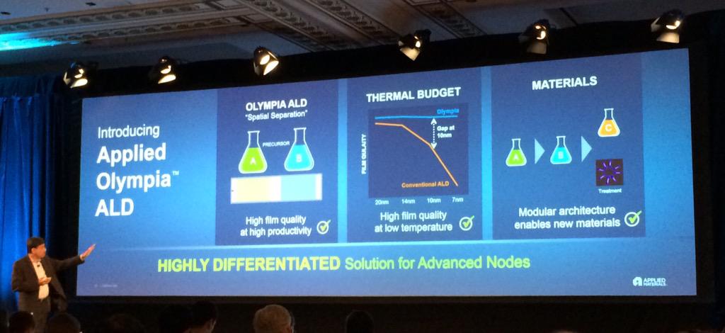
Cobalt is one of the most  important metals for leading edge BEOL Copper interconnects used for the processor chips in Smartphones, Tablets, PCs and Servers. In a modern highly scaled copper interconnect there are numerous opportunities for electromigration (EM) failure in the narrow copper lines, starting at line edges, at contact and via interfaces, and at CMP damaged surfaces. In addition, since grain growth is retarded in the smaller lines grain boundaries are becoming an increasingly significant electromigration failure mode. The focus is on very thin barriers that also act to inhibit EM at surfaces as well as alloy additions that can improve grain boundary EM. Of course, there are always tradeoffs, e.g. alloying the copper with something like Mn improves EM, but results in higher RS. Co as barrier and cap may also improve EM. Introduction of a Co liner and selective cobalt capping layer has demonstrated improved copper gap fill and an order-of-magnitude reduction in electromigration.  [TECHCET ALD/CVD Metal precursor report]

More details on the introduction of Co for Cu BEOL can be found in this article by Applied Materials published in Semicondtuctor Engineering [LINK].


According to news released by Umicore: Umicore is the first company in the world to have introduced a Sustainable Procurement Framework for Cobalt and is the first to obtain external validation for its ethical procurement approach in this area. It aims to minimize the risk of any connection between the cobalt in its supply chain – and subsequently that of its customers – and human rights abuses or unethical business practices. The framework builds on the specific approach to sustainable and ethical cobalt sourcing that Umicore introduced in 2004. Since then it has evolved to address specific risks linked to unethical mining practices, such as child labour and poor health and safety conditions. 

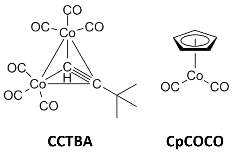
For CVD/ALD Umicore is offering two of the most used cobalt precursors within the  Sustainable Procurement Framework for Cobalt :

CCTBA : Hexacarbonyl(3,3-dimethyl-1-butyne)dicobalt [LINK]
CPCOCO : Dicarbonylcyclopentadienylcobalt(I), Co(CO)2Cp [LINK]


Why is a Sustainable Procurement Framework for Cobalt important?

Cobalt is classified as a so called conflict resource and these are natural resources extracted in a conflict zone and sold to perpetuate the fighting. In the case of Cobalt that is the ever ongoing conflict in Congo.
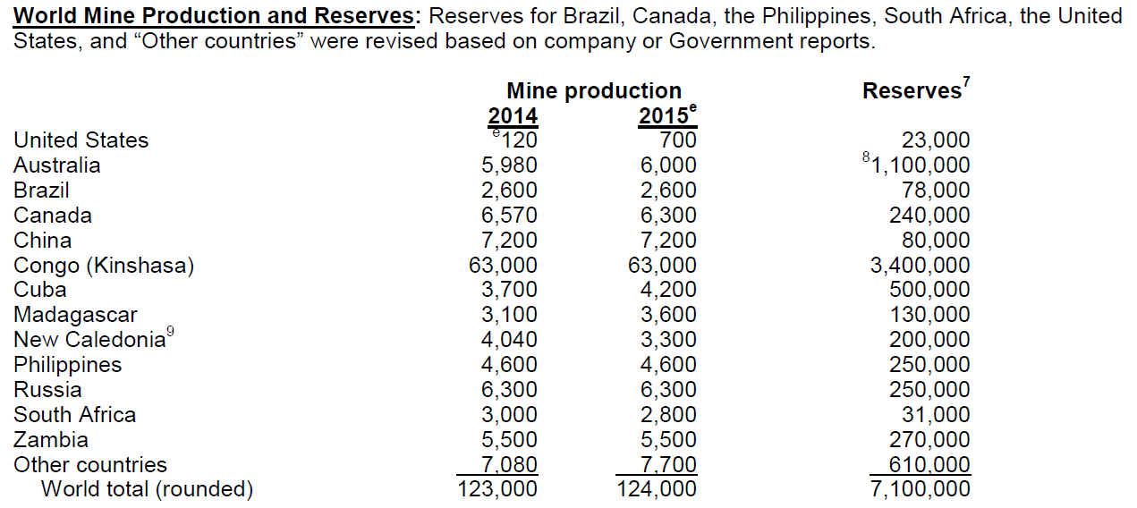
According to USGS 2016 Cobalt fact sheet the total identified world terrestrial cobalt resources are about 25 million tons. The vast majority of these resources are in sediment hosted stratiform copper deposits in Congo (Kinshasa) and Zambia ; nickel-bearing laterite deposits in Australia and nearby island countries and Cuba; and magmatic nickel-copper sulfide deposits hosted in mafic and ultramafic rocks in Australia, Canada, Russia, and the United States.

 
Besides the the Semiconductor industry and According to USGS : Cobalt is a metal used in numerous diverse commercial, industrial, and military applications, many of which are strategic and critical.  On a global basis, the leading use of cobalt is in rechargeable battery electrodes.  Superalloys, which are used to make parts for gas turbine engines, are another major use for cobalt.  Cobalt is also used to make airbags in automobiles; catalysts for the petroleum and chemical industries; cemented carbides (also called hardmetals) and diamond tools; corrosion- and wear-resistant alloys; drying agents for paints, varnishes, and inks; dyes and pigments; ground coats for porcelain enamels; high-speed steels; magnetic recording media; magnets; and steel-belted radial tires.

Sunday, December 18, 2016

Assessment of the Producer® Selectra™ etch system Applied introduced in June

Semiconductor industry analyst and CEO of VLSIresearch Inc., G. Dan Hutcheson published a video assessment of the Producer® Selectra™ etch system Applied introduced in June.


New Tech: Applied Materials' new etcher (embedded from www.youtube.com)

Summary: "Applied Materials' new Producer® Selectra™ Etcher is reviewed. It's billed as a Radically Different Etch Technology. Does it stand up to the claims? It this video, we examine why it really is radically different from a technical standpoint and is arguably the most innovative new etcher to be introduced since the early 1980s. The focus is on these questions: Why is Applied's Selectra important? What problems do Applied's Selectra attempt to solve? Does it enables next generation devices?"

Embedded Presentation from VLSI Research:


Applied Materials on Atomic Level Selective patterning technologies for 7 & 5 nm

Here is an interview with Prabu Raja, group vice president, fellow at Applied Materials and general manager for the Patterning and Packaging Group at Applied Materials, by Mark Lapedus at Semiconductor Engineering.


Prabu Raja, Group VP, Patterning & Packaging group, highlights Applied Materials Centris Sym3 Etch & Olympia ALD 2015 (Applied_Blog on Twitter)
The interview covers the upcoming hurdles like overlay and edge placement error in patterning at the 7 and 5 nm node and technologies to solve them:
  • Extreme ultraviolet (EUV) lithography
  • Self-aligned octuple patterning (SAOP)
  • Atomic Layer Etching (ALE)
  • Selective removal
  • Atomic Layer Deposition (ALD)
  • Selective deposition

Saturday, December 17, 2016

Abstract submission is open for ALD 2017

Abstract submission is open for ALD 2017  and the Abstract Deadline is February 17, 2017. The conference will take place Saturday, July 15-Tuesday, July 18, 2017, at the Sheraton Downtown Denver in Denver, Colorado, USA.

LINK : https://aldconference.avs.org/abstract-submission/


LG Display partner with Apple, Google and Microsoft for foldable OLED displays

Previously this year there have been a number of rumors that OLED display manufacturers will start using ALD barriers in production of next generation smartphone display. Now recent reports suggest that LG Display will start supplying foldable OLED displays for tablet sized smartphones (see tweet below) that can be folded to a typical smartphone format. Until now there has been no reports on ALD barriers for this one but one can assume that it is a good opportunity for ALD to be developed for these type of extreme display applications.


ETN News Reports : It is confirmed that LG Display has partnered up with Apple and google and is developing ‘out-foldable’ displays for Smartphones. It is going to start mass-producing them in 2018 and supply them to Apple, Google, and Microsoft. It is predicted that Samsung Display and LG Display will compete against each other in order to grab upper hands in markets for foldable displays.
According to an industry on the 15th, LG Display is currently developing out-foldable panels for Smartphones. Unlike how Samsung Display is working with Samsung Electronics’ Wireless Business Department, LG Display is developing foldable devices with outside businesses such as Apple, Google, and Microsoft.

Full story : LINK


Thursday, December 15, 2016

Fantastic industry support for the joint EuroCVD - Baltic ALD conference 2017 in Sweden

The joint EuroCVD - Baltic ALD 2017 in Sweden has got a fantastic interest form the industry with respect to sponsoring and exhibition so far.never seen before for the individual conferences. We hope that also all you highly devoted researchers submit awesome abstracts until 10th of January 2017.
God Jul & Gott Nytt År!
önskar
Henrik Pedersen, Sean Barry, Jonas Sundqvist and Mats Boman


Abstract Submission
Abstracts will only be accepted though the online abstract submission system, which will be available on November 10, 2016. The deadline for submission is January 10, 2017.

The abstract will consist of two parts: the extended abstract and the summary:
 
The extended abstract can be up to 2 A4 pages, and must follow the extended abstract template available below for download. Please download the template here (Word .docx format). Save the completed extended abstract as a .pdf for submission. Note: only .pdf files will be accepted in the online submission process.


"ALE has been lurking in the shadows for some time"

Following IEDM 2016 in San Fransisco - Here is a very nice overview of the leading ALE equipment supplier status and applications for FinFET & Gate-All-Around Transistors, 3DNAND, DRAM, Multiple Patterning by Jeff Dorsch, technology editor at Semiconductor Engineering. 

"ALE has been lurking in the shadows for some time. It was first patented in 1988, but even today it is not needed for many etch applications. Its key role is in 3D NAND flash memory devices, where high-selectivity etching is needed for the high-aspect ratios with the hard masks, along with the channel formation and the staircase contact."

OEMs covered:
  • Applied Materials
  • Lam research
  • Hitachi High Technologies
  • Tokyo Electron
Besides the Tier 1 OEMs you will also find ALE chambers from:
Having recently started ALE research myself  working with Plasway Technologies GmbH and Lund Nano Lab on some really cool stuff, it is a big mystery why the ALD OEMs does not move into this field. It can only be explained by that plasma processing is very difficult -  a lot of Voodoo! To start with you need wafer bias, which many PEALD chambers does not have and secondly ceramic chamber parts for plasma facing parts. Finally, reactive ion etching operates at much lower pressure and ALD OEMs does not typically integrate turbo pumps to their chambers. 
The next opportunity to learn all about ALE will be at the ALE2017 that is held in conjunction to ALD2017 : http://www2.avs.org/conferences/ALD/2017/

DATE & LOCATION:  July 15-18, 2017
Sheraton Denver, Denver, Colorado


Wednesday, December 14, 2016

High-Throughput, Cost-Effective Deposition via Atmospheric Pressure Spatial Atomic Layer Deposition

Here is a new paper on atmospheric Spatial ALD from Kevin Musselman and co-workers at University of Waterloo in Canada. According to information at The Waterloo Institute for Nanotechnology web: "Musselman helped pioneer the use of atmospheric pressure spatial atomic layer deposition (AP-SALD) thin films in optoelectronic devices. He used these films to address key questions in the field of energy conversion and to develop new optoelectronic devices. Musselman produced thin films of metal oxide alloys with tunable optoelectronic properties with which he probed loss mechanisms in colloidal quantum dot solar cells, ‘hybrid’ polymer-oxide solar cells and light emitting diodes, and all-oxide solar cells. These metal oxide films were also used to produce new, colour-pure “hybrid” organometal halide perovskite light-emitting diodes."

Nanomanufacturing: High-Throughput, Cost-Effective Deposition of Atomic Scale Thin Films via Atmospheric Pressure Spatial Atomic Layer Deposition

Kevin P. Musselman, Chukwuka F. Uzoma, and Michael S. Miller
Chemistry of Materials 2016 28 (23), 8443-8452
DOI: 10.1021/acs.chemmater.6b03077

Kick-off event HERALD ECI network at EuroCVD-BalticALD

Recently a network for Early Career Investigators (ECIs) has been formed within HERALD to help young ALD scientists to establish themselves and to stimulate collaborations. Our first event will take place at the joint EuroCVD-BalticALD conference, which will be held in Linköping, Sweden on June 11-14, 2017. At this conference there will be a section at the Tuesday poster session where the posters of ECIs will be grouped together, such that we can meet each other and discuss our work. Moreover, there will be a dinner for members of the ECI network on Wednesday evening (June 14) with time for more informal interaction. 

 
To sign up for this event, please submit an abstract at http://www.eurocvd-balticald2017.se/, and in the abstract submission system, tick the box “Abstract for the HERALD ECI poster session”. The poster can be a short overview of you and the projects you are working on, or a more conventional conference contribution. Even if you intend to give an oral presentation at the conference, we would appreciate it if you can also submit an abstract for the HERALD ECI poster section to introduce yourself to the network. The abstract deadline is January 10, 2017. Please register for the dinner by sending an email to ville.miikkulainen@helsinki.fi, and send any questions regarding the EuroCVD-BalticALD conference and the HERALD ECI poster session to henrik.pedersen@liu.se.

If you would not be able to join us in Linköping, but would like to be informed about other HERALD ECI events, please contact us using heraldeci@gmail.com.

The HERALD ECI committee is looking forward to your participation. 

Grow Low Temperature Nitrides by Atomic Layer Deposition Without Plasma


Unique Hydrazine formulation and package enables HAR and 3D film studies for Laboratories


At ALD Lab Saxony we have excellent previous experience with employing the RASIRC technology for dry hydrogen peroxide delivery in High-k ALD processes for PV and Logic applications. That is why we are very happy to announce that RASIRC from San Diego, California will be sponsoring, attending and exhibiting at ALD for Industry 17-18th of January in Dresden Germany. This is an excellent opportunity to meet RASIRC and learn about their latest product release for safe and effective delivery of hydrazine for Atomic Level Processing. Please find the product fact sheet below.

RASIRC BRUTE® Hydrazine - Laboratory Version is specifically designed for universities and research institutes in development of Atomic Layer Deposition and Etch (ALD and ALE) processes with compressed thermal budgets. Hydrazine molecules can enable low temperature metal nitridation, opening up many potential avenues for advancements in High Aspect Ratio (HAR) and three dimensional structures grown via ALD and ALE.

“This new vaporizer package should enable researchers to investigate low temperature thermal nitride processes without a large budget.” - Jeff Spiegelman President and CEO of RASIRC.


Scientists working with TiNx, TaNx, SiNx, WNx, Platinum, Palladium, Cobalt or other new materials can benefit from using BRUTE Hydrazine. Additional benefits may be found from the generation of radical hydrogen and limited etching and surface cleaning effects. 


Figure 1: BRUTE Hydrazine (50ml). Based on RASIRC Drawing #202268

BRUTE Hydrazine delivers water-free hydrazine gas (N2H4) to process in a controlled, repeatable manner. Preloaded in a non-volatile solvent, the Brute Hydrazine chemistry is packaged in a single use vaporizer (Figure 1) with metal seals, making hydrazine gas simple to connect and deliver. 

Benefits of the Laboratory Version 

  • Sized for universities and research labs
  • Improved safety—RASIRC patent pending solvent delivery system raises the flash point
  • Simple plug-and-play design with a single connection to the vaporizer
  • Direct vacuum draw
  • Manual operation
  • Less chemistry than industrial ampoules, improving safety
  • Low cost
  • Smaller footprint

BRUTE Hydrazine Applications

BRUTE Hydrazine can be used for a wide range of low temperature processes including ALD, ALE, MOCVD and nitride materials development:
  • Contact barrier and other memory applications using TiN and TaNx
  • Precursor for TiN gate stack and other transistor applications
  • Sidewall spacer/etch stop (SiNx) between metals and silicon or dielectric materials
  • Multiple patterning involving SiO2 and SiNx
  • Selective deposition and etch involving metal nitrides and SiO2
  • SiGe passivation involving SiNx, SiOxNy and BN
  • Metal nitride deposition (WNx)
  • Low temperature metal oxide reduction for metal ALD (Co, Cu, Pd, Pt)
  • Atomic removal of surface carbon

Enables New Material

Plasma and ammonia-based methods fail to meet next generation process requirements for lower thermal budgets and ability to act deep within high aspect ratio or 3D structures.
  • Plasma cannot uniformly coat the sidewalls of high aspect ratio structures and can cause surface damage
  • Ammonia (NH3) has limited reactivity at low process temperatures, which leads to poor film quality
  • Standard High Purity Hydrazine has measurable water that leads to oxygen incorporation in nitride films increasing film resistance
BRUTE Hydrazine solves these problems. 


Figure 2: Theoretical Vapor Pressure Curve of BRUTE Hydrazine

BRUTE Hydrazine Characteristics

  • Dry (less than 50 ppm H2O in the liquid source), resulting in minimal oxygen contamination
  • Higher reactivity than NH3, enabling lower temperature ALD applications (200-400°C)
  • Better penetration of high aspect ratio structures, creating uniform films

How it Works

BRUTE Hydrazine provides a stable, reliable flow of anhydrous hydrazine gas from a liquid source in a metal sealed vaporizer (Figure 1). The liquid source combines anhydrous hydrazine and a proprietary non-volatile solvent, significantly increasing the flashpoint. This makes the chemistry safer to handle than anhydrous hydrazine. To deliver hydrazine gas to process, vacuum is applied to the BRUTE Hydrazine vaporizer to evaporate liquid BRUTE Hydrazine to pure hydrazine, leaving the non-volatile solvent behind. The Theoretical Vapor Pressure Curve of BRUTE Hydrazine is given in Figure 2.

How to Order

To place an order for 50ml BRUTE Hydrazine contact RASIRC at sales@rasirc.com and order P/N: 100784.

 
RASIRC specializes in products that generate and deliver gas to fabrication processes. Each unit is a dynamic gas plant in a box - converting common liquid chemistries into safer and more reliable gas flow for most processes. First to generate ultra-high purity (UHP) steam from de-ionized water, RASIRC technology can now also deliver hydrogen peroxide gas and hydrazine gas in controlled, repeatable concentrations. RASIRC gas delivery systems, humidifiers, and closed loop humidification systems are critical for many applications in semiconductor, photovoltaic, pharmaceutical, medical, biological, fuel cell, and power industries.