Sunday, July 31, 2016

Trends in plasma-enhanced atomic layer deposition

The mysterious Plasma ALD Guy (PAG) had a great time at ALD 2016 this past week. PAG presented a poster on Tuesday evening that was enjoyed by many. If you missed it, you can check it out here.


Based on the review 2013 to 2015 South Korea is in the lead judging by the number of PEALD publications followed by USA and Germany. Striking is the lack of PEALD publications coming from the leading ALD centers of Helsinki University, VTT and Aalto University.

The other observation is that >75% of all PEALD is performed for pretty basic ALD materials (Al2O3, AlN, TiO2) using basic ALD precursors like TMA. The Finnish ALD community has a strong tradition of focusing on new precursor chemistries and new materials and that may be an explanation why PEALD is not in the focus there.

You also see that Turkey is very strong represented in this field. Unfortunately many of the Turkish Scientists were not allowed to participate in ALD2016.

Saturday, July 30, 2016

Winners of the ALD2016 Twitter competition - The #ALDToughGirls

Prof. Henrik Pedersen from Linköping university in Sweden won the Twitter competition at ALD2016. He tweeded actively and managed to cover all aspects of the conference - Scientiffically and Socially and personal funny observations. He also made the innoficial #ALDToughGuys vs. #ALDToughGirls competition go to the girls this time. Maybe ALD2017 will have mixed teams #ALDToughScientists instead?


Photos from ALD.com and Twitter.com

Honor should also go to Miia Mäntymäki for being the first Tough Girl on twitter. Later she enjoyed GTs with the toughest of all ALD Scientists, Tero Pilvi from Picosun at the Airport. He can chew gum and talk Swedish at the same time - it is a self-limmited process.

Photo from Tero Pilvi at facebook.com, the moment just before starting to talk Swedish...

Pico Party (twitter.com)

Some asorted looser ALD Tough Guys below:


Pictures from Twitter.com #ALDToughGuys

Wayne State presented new ALD chemistries for low temperature tantalum and selective cobalt at ALD2016

Prof. Chuck Winter and his team at Wayne State presented new ALD chemistries for low temperature tantalum and selective cobalt at ALD 2016 Ireland this week. Both processes are very important for todays scaling of logic and memory technologies. Metallic tantalum can be used in workfunction engineering of HKMG high performance FinFET transitors as well as for Cu seed/barrier technology in BEOL. Cobalt is as tantantlum an option for Cu barrier/seed and also used selectivly to cap the Cu lines and vias from oxidising and reducing RC performance.


The best highlight talk went to Marissa Kerrigan from Wayne State as voted by attendees on novel Co recursor chemistry for selective Cobalt (Left Marissa Kerrigan, right Simon Elliott, photo by ALD2016.com).

“This opens up the prospect of using tantalum in layers just a few nanometers thick as the liner for interconnect wiring in the complex geometries of next-generation electronic chips,” said the University, which worked with German chemicals giant BASF on the project accoring to Electronic Weekly.

Marissa Kerrigan also from Wayne State announced novel ALD chemistry for metallic cobalt that showed excellent selectivity to copper (photo by ALD2016.com).

“The Wayne State processes for tantalum and cobalt are significant steps forward in controlled growth of ultra-thin metals,” said conference chair, Dr Simon Elliott of Ireland’s Tyndall National Institute. “Strong growth is projected for area-selective deposition: in the near future, it will allow higher-precision patterning of semiconductor chips, and in the longer term it will be an enabler for manufacturing nano-structured materials on demand.” according to the same article in Electronics Weekly.

ALD History Blog: ALD history at ALD 2016 Ireland

ALD History Blog: ALD history at ALD 2016 Ireland: Prof Greg Parsons introducing Prof Anatoly Malygin to give a plenary talk at ALD 2016. Photo by Riikka Puurunen. The  ALD 2016  confer...

Friday, July 29, 2016

A breakthrough in Spatial ALD by Dutch research team at HOLST Centre presented at ALD2016 Ireland

A breakthrough materials processing technique devised by a Dutch research team could lead the way for a new generation of smart fabrics, wearable electronics, solar cells and flat-panel displays.

Many of these technologies work by sandwiching together layers of different materials, with some layers ten thousand times thinner than a sheet of paper (just a few nanometres). Such thin layers can be laid down by a technique called atomic layer deposition (ALD), which is the subject of the new research by Holst Centre/TNO in the Netherlands. Improving how the thin layers are deposited is opening up many new opportunities and applications for flexible electronics in everyday life.

ALD is a highly precise technique for the growth of thin material layers. It is primarily used in the fabrication of electronic chips for an array of consumer products such as PCs, tablets and smartphones. Ultra-thin ALD layers in these devices deliver improved speed, energy efficiency, resolution and memory capacity.

The ALD processes used in the semiconductor industry are precise but slow, depositing roughly one nanometre per minute, and must be carried out in specialised vacuum equipment at low pressure on rigid materials. This is acceptable for making chips in the semiconductor industry, but is an obstacle towards using ALD for coating fabrics, foils or TV displays in a standard factory environment. 

 The research team at Holst Centre/TNO, led by Dr Paul Poodt, has successfully brought ALD out of the vacuum to atmospheric pressure, and shortened deposition times to nanometres per second, without compromising on quality. They achieved this by switching to ‘Spatial ALD’ on large-area and roll-to-roll factory equipment that is suitable for coating flexible films and large sheets. (Picture from LinkedIn.com)

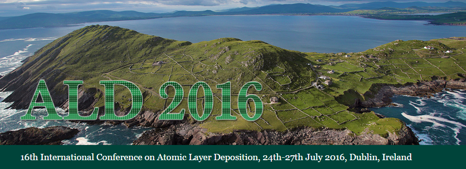
The new technique is one of a number of thin film innovations being presented at the 16th International Conference on Atomic Layer Deposition (ALD 2016), which takes place in the Convention Centre Dublin, Ireland on July 24-27.

The team at Holst Centre/TNO started research into Spatial ALD in 2009 and have successfully shown its use in many applications, including a higher efficiency solar cell that is now on the market. Their current goal of coating porous materials and polymers is even more challenging, but could be hugely rewarding.

Paul Poodt, Program Manager at the Open Innovation Institute Holst Centre said: “We needed to understand the role played by gas pressure in Spatial ALD. Porous materials are like microscopic sponges, and molecules need to travel through all the pores, nooks and crannies before coating the pores properly. We found simple equations that tell us that atmospheric pressure does not in fact slow down ALD in porous materials, but can actually help to speed it up. With this understanding we can make clever designs of new Spatial ALD reactors.”

Dr Poodt added: “We believe that Spatial ALD will make flexible electronics possible soon – useful technologies like foldable displays, wearable phones and smart fabrics. We hope that the results we present at the ALD2016 Conference will be the first step to a new range of applications where Spatial ALD can be a key enabling technology.”

Dr Simon Elliott from Tyndall National Institute, chair of the ALD2016 Conference, said: “This exciting result from TNO is a great example of how seemingly-abstract theoretical understanding of gas flow past obstacles can directly impact on the manufacture of new high-tech devices, such as (O)LED lighting, flexible displays and miniature batteries for wearables.”
Dr Paul Poodt and his team will be presenting their research findings on accelerated growth of thin films onto flexible materials as part of the ALD2016 Conference in Dublin. For further information about the ALD2016 Conference please see http://ald2016.com/


TECHCET Reports Record Silicon Wafer Shipments

TECHCET reports - The silicon demand outlook for 2016 expected to increase of 6.8% to 11.1 BSI, largely due to the strength of the memory market. Regardless of overall wafer consumption, Issues with wafer supply will likely continue, as demand for 300mm polished wafers increases beyond capacity, while epitaxial wafer supply at that diameter remains in excess. Certain 200mm wafers are also in a tight supply situation given strong demand growth from the discrete device fabs coupled with limited supplier capacity, as explained in by Mike Walden, of TECHCET CA. Their recent report further indicates that declining ASPs are expected as competition for China's 200mm wafer demand increases and the 300mm market continues its evolution toward polished wafer usage. 


Although shipments of silicon by area recovered after 2009, prices have still not recovered to 2008 (pre-US housing / WW credit crisis) levels. Silicon area shipments were relatively flat from 2010 through 2013 before rising 10% in 2014. Meanwhile, silicon revenue peaked in 2010-2011 before declining sharply in 2012 and 2013 to begin 4 stagnant years. TECHCET expects aggregate Si ASPs to fall slightly in 2016 before firming or modestly increasing in 2017. Also noted by Walden, "China will have a major influence on this market in the years to come".

For more detailed information and added insight on SOI, China and 450mm wafers, the reader is referred to TECHCET's Critical Materials Report(TM) on the Silicon Wafer Market and Supply Chain.
For more information, please contact info@techcet.com 
or call 1-480-382-8336
 
* Interested in learning more about Membership to the
Critical Materials Council and/or China's supply chain? 
Join the November CMC Meeting in China!

Thursday, July 28, 2016

ASMi ALD Equipment Status & Forecast for growth in 2017

ASM Intertnational released their Q2/2016 report today and here below is the ALD Market Outlook according to ASMi. The Earnings call will be tomorrow so possibly more interesting information will be given then.


  • 2015 has shown a strong growth of the single wafer ALD market. We estimate this growth to continue whereby the single wafer ALD equipment market will double in the period 2015-2018/2019. We however expect the single wafer ALD market to show a double digit decline in 2016, caused by a low demand in Memory which will not be offset by the strong increase in Logic/Foundries. Our single wafer ALD market share is expected to show an increase in 2016. We expect the single wafer ALD market to strongly improve again in 2017.
  • In Memory, the NAND market is shifting from Planar NAND to 3D NAND. This shift will significantly reduce the demand for additional multi patterning-related single wafer ALD capacity. Non-patterning related single wafer ALD demand is expected to gradually increase as soon as next generation 3D NAND is going to ramp into high volume. 
  • In Memory, DRAM industry capacity demand was high in 2015 and has declined strongly in 2016. Based on current visibility the demand for new DRAM-related single wafer ALD capacity is believed to recover earliest in the course of 2017. 
  • In Logic/Foundry the transition to the 10 nm technology node fuels substantially higher single wafer ALD-equipment demand than the previous nodes.

Increasing Demand for Atomic Layer Deposition (ALD) Equipment

Here is a new Market Research report on ALD Equipment from TMR forecasting a continued increase in sales of ALD equipment. This is consistent with other reporting from VLSI Research, Gartner and ASM International. However, this report also claim that export control, lack of ALD experts, and slow dep rate may limit growth. Just returning from ALD 2016 Ireland and the Industry Panel we had there - I do not see that a lack of ALD professionals may be an issue - but who knows maybe that´s the case - so it would be very interesting to know others view on this.

"The absence of skilled human resource and the slow deposition rate of ALD equipment are also likely to curb growth to some extent."


The presence of a large number of international and local companies is boosting competition in the global atomic layer deposition (ALD) equipment market. As per a new study by Transparency Market Research (TMR), the competition prevailing in the market is expected to intensify further between 2016 and 2024. As of 2015, ASM International N.V., Applied Materials, Inc., and Tokyo Electron Ltd. cumulatively held a share of 58.9% in the global market. Of these, ASM International N.V. emerged as the top player, accounting for over 28% of the global ALD equipment market in 2015. Rivalry among key players in terms of product development and technology and product upgrades is expected to intensify during the forecast period.

"Due to the recent advancements in the atomic layer deposition technology, the use of ALD equipment has considerably increased in the nanotechnology sector," says a lead analyst at TMR. TMR expects applications of ALD equipment as manipulation and fabrication tools in nanotechnology to rise further in the short term. "Growing concerns pertaining to carbon emissions have accelerated investment in the R&D of photovoltaics. Due to the increasing research and development activities, the use of ALD as a PV manufacturing method has substantially expanded," adds the analyst. This rising demand for photovoltaic cells, combined with rapid advancements witnessed in PV technology, will subsequently augment sales of ALD equipment in the forthcoming years.