Showing posts sorted by relevance for query selective. Sort by date Show all posts

Saturday, April 18, 2015

ALD-enabled nano-patterning

Here is a very good text by Mark Lapedus on ALD patterning technology from the Semiconductor Engineering Blog:

Selective deposition may be the way forward to the far reaches of device scaling after 7nm.
APRIL 16TH, 2015 - BY: MARK LAPEDUS


Chip scaling is becoming more difficult at each process node, but the industry continues to find new and innovative ways to solve the problems at every turn. And so chipmakers continue to march down the various process nodes. But the question is for how much longer? In fact, at 16nm/14nm and beyond, chipmakers are finding new and different challenges, which, in turn, could slow IC scaling or bring it to a sudden halt one day.

To prevent those occurrences, chipmakers are working on a multitude of technologies. But one in particular is gaining steam in the lab—selective deposition. Some call the technology ALD-enabled nano-patterning.

At least in theory, selective deposition is a paradigm shift in chip manufacturing that could help extend IC scaling. But researchers still have some issues to solve to make this technology viable. And even then, it is not expected to appear until 7nm or 5nm.

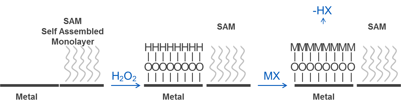
For decades, chipmakers have used deposition, which is a process that deposits a blanket of thin material on a surface. In contrast, combining novel chemistries with atomic layer deposition (ALD) or molecular layer deposition (MLD) tools, selective deposition involves a process of depositing materials and films in exact places. Selective deposition can be used to deposit metals on metals and dielectrics on dielectrics on a device.


Please also do check out this Review, that I have blogged about before, by Prof. Kessels et al on this topic!

A. J. M. Mackus, A. A. Bol and W. M. M. Kessels
Nanoscale, 2014,6, 10941-10960 
DOI: 10.1039/C4NR01954G, Review Article

Atomic layer deposition (ALD) is a method that allows for the deposition of thin films with atomic level control of the thickness and an excellent conformality on 3-dimensional surfaces. In recent years, ALD has been implemented in many applications in microelectronics, for which often a patterned film instead of full area coverage is required. This article reviews several approaches for the patterning of ALD-grown films. In addition to conventional methods relying on etching, there has been much interest in nanopatterning by area-selective ALD. Area-selective approaches can eliminate compatibility issues associated with the use of etchants, lift-off chemicals, or resist films. Moreover, the use of ALD as an enabling technology in advanced nanopatterning methods such as spacer defined double patterning or block copolymer lithography is discussed, as well as the application of selective ALD in self-aligned fabrication schemes.

Friday, February 26, 2021

Area-selective MLD of nylon 6: Growth on carbon and inhibition on silica for a-carbon hardmask repair

Here one of the Editor pic out of the JVSTA Special Topic Collection on Area Selective Deposition. Marcel Junige, is one of Dresden´s top-notch ALD and MLD scientists that went over there to the University of Colorado Boulder to S M Geroge´s famous lab. In this demonstration, it is illustrated the capability of area-selective MLD to repair RIE-eroded aC hard masks and to maintain the critical dimension, which is key in all leading etch semiconductor manufacturing processing schemes. It is a fairly typical situation in this business, the CMP or Etch guys brutally destroy stuff that has to be repaired by ALD or Wet processing, sometimes even by E-Beam single exposure repair. That is maybe one of the drivers behind the more precise and gentle ALE method. Yeah E-CMP ever made it.

Area-selective molecular layer deposition of nylon 6,2 polyamide: Growth on carbon and inhibition on silica

Journal of Vacuum Science & Technology A 39, 023204 (2021); https://doi.org/10.1116/6.0000769
Marcel Junige and Steven M. George


In microelectronic or nanoelectronic manufacturing, pattern transfer by directional reactive ion etching (RIE) progressively erodes amorphous carbon (aC) hard masks. To maintain critical dimensions and tolerances of high-aspect-ratio device structures, new carbonaceous materials may be added repeatedly to replace the eroded aC hard mask. Such a mask repairing step during RIE needs self-aligning growth of organic materials. Area selectivity is required to deposit the organic material on the aC hard mask exclusively. Deposition on the dielectric or semiconductor device structures underlying the mask would complicate their precise etching or later cleaning. When ashing the aC hard mask, all-organic materials are preferable to organic-inorganic hybrid materials because they leave no residue. In this work, area-selective molecular layer deposition (MLD) was developed for the all-organic polyamide nylon 6,2. The monomer reactants for nylon 6,2 MLD were ethylene diamine and adipoyl chloride. Nylon 6,2 MLD was studied in the homogeneous, steady-state growth regime and during nucleation on various starting surfaces utilizing in situ spectroscopic ellipsometry. Area-selective MLD of nylon 6,2 was achieved on the “growth” carbon surface in the presence of silica by functionalizing aC via mild oxidation. In addition, a surface passivant was selectively attached to silica by using an amine-catalyzed coupling chemistry. The passivant inhibited the nylon 6,2 MLD on the “nongrowth” silica surface. A single passivation pretreatment was sufficient to restrict the MLD on the silica surface. The passivant, however, did not substantially impact the MLD nucleation and growth on the aC surface. This strategy yielded area selectivity with exceptionally high quality and over a wide range of MLD cycles. The area-selective MLD of nylon 6,2 was further applied on industrial test features with aC patterns masking trenches in silica. This demonstration illustrated the capability of area-selective MLD to repair RIE-eroded aC hard masks and to maintain the critical dimension.


Tuesday, June 12, 2018

Report from the 3rd Area Selective Deposition Workshop (ASD 2018) at North Carolina State University

In late April (April 29 – May 1, 2018) the 3rd Area Selective Deposition Workshop (ASD 2018), was held at North Carolina State University in Raleigh North Carolina USA (LINK). This years workshop was organized with full support from AVS and as for ALD and ALE Della Miller was in charge.

The Workshop brought together leading international scientists and engineers from academia and industry from all regions to share results and insights into: 1) fundamental principles and barriers to area selective deposition; 2) technological needs and challenges of ASD; 3) new chemical approaches and processes to address the expanding needs; and 4) surface characterization techniques and metrology innovation for ASD.

This third year the program was expanded to two days, including 11 invited presentations, an invited panel discussion, 18 contributed talks, and 15 posters and in between there was plenty of time for interaction over meals and social events.

ASD2018 brought together leading experts from 10 countries in Asia, Europe and America, to deliver and discuss more than 45 presentations. As the chart shows, this constitutes significant growth since the first ASD Workshop in 2016 (ASD2018 Book of Abstracts).

As a particular focus this year, the committee had chosen to highlight the challenge of selective deposition metrology, including an invited panel to discuss particular issues and techniques related to selectivity measurement and selective defect quantification.

It is clear that ASD is a fast growing field and may at some point in time reach the status as a stand alone segment with respect to processing, chemicals and equipment. Another indication can be seen that at the SPIE in February there was a high number of presentations and posters on combining ALD and ALE or just Area Selective Deposition.

Program Char Prof. Gregory N. Parsons of North Carolina State University, USA has asked to share some photos form the successful event (below). In addition, an article covering the event was just published by Chemical & Engineering News (LINK) including interviews and the latest insights from Dennis M. Hausmann (Lam Research), Gregory N. Parsons, Silvia Armini (invited speaker, imec), Dara Bobb-Semple and Stacey F. Bent (Stanford University), and Steven M. George (Colorado Boulder University).

Studying the Book of Abstract, my personal favorite is the atmospheric pressure micro-plasma printer for area-selective ALD presented by Prof. Kessels (TU Eindhoven). This technology is being commercialized by the Dutch company with InnoPhysics (LINK) and you can expect to hear more details about this exciting technology soon.

Rear view from the The StateView Hotel conference room (Photo: Gregory N. Parsons).
Junling Lu from University of Science and Technology of China, Hefei presenting "Bottom-up Engineering Catalyst Nanostructures using Area-Selective Atomic Layer Deposition" (Photo: Gregory N. Parsons).

Wednesday, March 16, 2022

AVS ASD 2022 April 21-22 - Technical program


Technical Program
Reserve Hotel by March 25
We have arranged a special conference rate at the Westin St. Francis. Keep in mind that reserving a room in the conference hotel block is important because it helps ASD meet its financial commitments to the host city and retain lower registration fees as well as a high quality conference with the features and services you are accustomed too.

Due to limited space we recommend booking as early as possible to receive this special rate—please note that once the reserved/contracted room block is full, the room availability and rate are not guaranteed and may vary.

If your dates are not available, please contact Alberto Lamberti at 1-415-774-0122, alberto.lamberti@westin.com for help.
In an effort to help facilitate the progression of ASD techniques, the 6th Area Selective Deposition Workshop (ASD 2022) scheduled for April 21-22, 2022, in San Francisco will act as a central event for sharing and discussing the newest developments in ASD by gathering leading experts from both academia and industry. Attendees can expect to participate in talks regarding fundamental challenges related to recent developments in ASD, applications for ASD in next-generation technology, emergent processes for implementing ASD techniques, and new perspectives on metrological and characterization strategies for further understanding persistent mechanistic challenges. Based on the success of the previous workshops, ASD 2022 will consist of two days of presentations by invited and contributing speakers, as well as a banquet reception and poster session.
Invited Speakers:

  • Keynote Speaker - Stacey Bent (Stanford University, USA), "Next Generation Nanopatterning Using Area Selective Deposition”
  • Cathleen Crudden (Queen's University, Canada), "N-heterocyclic Carbenes in Selective Area Deposition"
  • Jolien Dendooven (Ghent University, The Netherlands), "In-situ Studies of Nucleation Mechanisms during ALD of Platinum-Group Metals"
  • Damon Farmer (IBM Research, USA), "Inhibitor-Free Nucleation Inhibition of Superconductors"
  • Padma Gopalan (University of Wisconsin, USA), "Carbon Nanotube Selective Deposition"
  • Andrew Kummel (University of California San Diego), "Selective Atomic Layer Deposition of MoSiX"
  • Mikko Ritala (University of Helsinki, Finland), "Area-Selective Etching of Polymers, a Novel Approach to Self-Aligned Patterning of Thin Films"
  • Frances Ross (Massachusetts Institute of Technology, USA), "In Situ Electron Microscopy to Visualize Crystal Growth Mechanisms on Plain and Patterned Surfaces"
  • Bonggeun Shong (Hongik University, South Korea), "Theoretical Understanding on the Principles of Area-Selective Atomic Layer Deposition"
Topics:
This event is centered on showcasing developments across the whole spectrum of area-selective deposition. Thus, the Workshop will cover a wide range of topics including the following:

  • Near Term Technology Readiness (Scalable and Relevant ASD Processes for Use in Manufacturing)
  • Fundamentals of ASD (Defects, Growth Mechanisms and Inhibitor Chemistries)
  • Metrology Techniques for ASD
  • Emerging/Exploratory ASD Processes and Applications (e.g., Catalysis, Energy Generation and Storage)
Program Chair:
Rudy J. Wojtecki
IBM Almaden Research Center, USA
Questions? Contact rjwojtec@us.ibm.com

Friday, November 20, 2015

Can ALD save Moore´s Law?

Can ALD save Moore´s Law? - I would say it already did at the introduction og HKMG and some other things. Here is a great peace by Mark Lapedus with some insights from the leading extperts of industry and academia and I selected to high light some of them below:

Can Nano-Patterning Save Moore’s Law?

Selective deposition is showing promise in the lab, but it’s a long way from there to production.

For years the academic community has explored a novel technology called selective deposition. Then, more than a year ago, Intel spearheaded an effort to bring the technology from the lab to the fab at 7nm or 5nm. Today, selective deposition is still in R&D, but it is gaining momentum in the industry.


 “In order to make ALD-enabled nano-patterning available in the semiconductor industry, careful ALD precursor and reactant selections are required,” Samsung’s Han Jin Lim said.  


“There are a couple of places where selective deposition has been done in the past. But the applications have been pretty specific, where we have gotten our arms around the defectivity issues,” said Dave Hemker, senior vice president and chief technology officer at Lam Research. “But anytime you go selective and deposition, you’ve have to make sure the defectivity and other issues are solved. As we learn more about it, we’ll see more applications coming out of it.”


“With SAM, it might be possible to do selective-area ALD or CVD by area-deactivation,” said Erwin Kessels, a professor at the Eindhoven University of Technology. “But this only provides a solution in cases where the substrate is already patterned. Selective deposition by area-deactivation doesn’t really help you in most cases when you really want to generate patterns from the bottom-up, which is the ultimate aim. Yet, it would still be helpful to reduce the number of litho steps.”

Continue reading : http://semiengineering.com/can-nano-patterning-save-moores-law/ 

Tuesday, February 2, 2016

UPDATE: Area Selective Deposition Workshop - ASD 2016 hosted by Imec

Imec and the COST action HERALD will host a workshop dedicated to Area Selective Deposition “ASD 2016”, at imec in Leuven, Belgium on April 15th, 2016. This workshop will provide an excellent opportunity for the R&D community to learn about Area Selective Deposition and it will offer a forum for open discussions between researchers from academia and industry. We look forward to your participation.


The workshop will focus on the fundamental mechanisms of ASD processes and nucleation, as well as on the challenges related to the characterization of selectivity. Potential applications of selective deposition will be discussed.


The 1 day program will consist of:
  • Presentations by invited speakers on the fundamentals and characterization of selectivity
  • A panel discussion about potential applications of selective deposition
  • A poster session covering selective deposition as well as nucleation. Poster contributions are welcome by abstract submission
  • Coffee breaks, lunch and diner
Confirmed invited speakers: 
Soley Ozer (Intel), Mikko Ritala (Helsinki University), Erwin Kessels (TU Eindhoven), Simon Elliott (Tyndall National Institute), Gregory Parsons (North Caroline State University), Christos Takoudis (University of Illinois at Chicago), Hyungjun Kim (Yonsei University), Wilfried Vandervorst (imec), Manfred Buck (St Andrews University), Jim Engstrom (Cornell University)
Registration module is open - Deadline: March 25th, 2016.
- Poster contributions are welcome by abstract submission (see website). Deadline: March 15th, 2016. The poster session is covering area-selective deposition as well as nucleation.
- HERALD travel support: HERALD members can apply for travel support by sending a short motivation letter and CV to asd2016@imec.be. Deadline: March 2nd, 2016.


More information is available at http://www2.imec.be/be_en//education/conferences/asd-workshop-2016.html

Monday, April 5, 2021

Intermolecular at the AVS ASD2021 Workshop, April 6-8.

Join Milind Weling as he talks with fellow panelists Robert D. Clark (TEL) Annelies Delabie (imec), Adrie Mackus (Eindhoven University of Technology) Anuja De Silva (Lam) on Area Selective Deposition at ASD2021 on April 8 at 12:50PM CDT, 10:50 AM Pacific. Moderated by Rudy Wojtecki (IBM).


Join EMD Electronics and program co-chairs John Ekerdt & Stacey Bent at the Area Selective Deposition Workshop, April 6-8.

Day 1: April 6
Poster Session at 2 pm • Lanxia Cheng presents “Area Selective Deposition of Electronics using Multilayer SAM as Surface Passivation.”

Day 2: April 7
Session 4 is chaired by Ravindra Kanjolia., EMD Electronics

Poster Session at 2 pm • Lanxia Cheng presents “Area Selective Deposition of Electronics using Multilayer SAM as Surface Passivation.”

Day 3: April 8
Session 8 at 11:30 am • Ravindra Kanjolia presents, EMD Electronics “Strategies for Area Selective Deposition: From Inherently Selective Precursors to Inhibitor Molecules and Processes.”

12:50 pm • Milind Weling participates on a panel discussion “Area Selective Deposition.”

Tuesday, April 24, 2018

RASIRC to Present Anhydrous Hydrogen Peroxide Surface Preparation and Enhanced Nucleation for ASD at ASD2018

Area selective deposition is becoming increasingly important for the immense scaling effort continuously taking place in the semiconductor industry for Logic and Memory Devices. Today double and multiple pattering schemes using Plasma Enhanced ALD are in High Volume Manufacturing (HVM) for all sub 28 nm nodes and any moment now the industry expect to ramp EUV lithography, possibly at the 7 nm Foundry Node. Beyond that in a joint effort the researchers and the industry are looking for alternative patterning methods and many of them are based on so called bottom-up patterning.

To put things in perspective for ASD, one of the first area selective ALD processes in HVM was introduced in 300 mm DRAM manufacturing by Infineon Technologies in 2004 (90 nm Deep Trench DRAM presented in detail at IEDM 2004). This area selective ALD process relied on controlling the amount of hydroxyl groups in the upper part of a trench structure using the well-known TMA / H2O based process growing Al2O3. The goal was to let the process partially penetrate about 1 micron deep into very deep DRAM trenches to protect the silicon surface from a following isotropic etch that would widen the deep trench creating more surface and therefore allow a higher capacitance of the memory cell which is a key performance parameter in DRAM at about 25 fF/cell at that time.

In addition, the liner protected the collar region from dopant penetration keeping a well-defined dopant profile isolated from the wafer surface where the select transistor would later operate and it also defined a selective area for growth of Hemi-Spherical Grains (HSGs) another surface area expansion technology used in the DRAM industry. Please check the patent visualized below for many more details. This fascinating process was Self-Aligned and Area Selective in so many ways and kicked out a number of complex alternative integration paths saving a lot of $/wafer. By optimizing all process parameters it was possible to control the penetration depth of the liner, the transition region length down to the non-growth area, wafer uniformity and liner quality (density). This process was used until the end of the Deep Trench era which at this time had ~25% of the DRAM market but was killed at 65 nm when all companies had transitioned to stacked memory cells.

The Non-conformal ALD Al2O3 liner application as described in the US patent “Process for vertically patterning substrates in semiconductor process technology by means of inconformal deposition” (Figure from US7344953B2) 


Since then several things have happened. For one thing ALD has become a standard processing technology in Logic and Memory HVM forming its own Business Segment with an annual Equipment revenue >USD 1.5 Billion. Secondly, Atomic Layer Etching (ALE) has also entered HVM at the Logic 14 nm FinFET manufacturing. In parallel several efforts have begun to explore novel methods for ASD. These utilize Self-Assembled Monolayers, Patterned Photoresists, Selective CVD processes (e.g. Cobalt CVD), Plasma deposited films and other creative surface blocking agents and employing ALD and ALE in combination to trigger or block surface growth.  In parallel, reactive surfaces must be created for high nucleation and growth of metal oxide films.  An ideal surface treatment for the latter will:

                  Create high density surface functionalization
                  Have zero or minimal sub-surface oxidation
                  Lead to faster and more uniform nucleation versus H2O
                  Remain non-reactive with organic functionality or photoresist on adjacent surfaces

The use of the novel reactive chemistry, anhydrous hydrogen peroxide, has been largely ignored. This is due to: a lack of literature precedent; that H2O2 is typically delivered with H2O (multiple publications from K. Kukli et al at University of Helsinki and Tartu) where water dominates the reaction chemistry; and that only recently did this material become available by RASIRC (San Diego, USA) in an ampoule form that could be integrated into ASD process equipment.

Besides water, Ozone is an important co-reactant and oxidative precursor in ALD of metal oxides for, e.g., High-k dielectrics in DRAM Capacitors. Hydrogen Peroxide has similar oxidation properties to Ozone (oxidation potential O3 = 2.1V versus 1.8V for H2O2) while simultaneously having slightly stronger proton transfer properties than water (water pKa = 7.0 versus 6.5 for H2O2). According to Jeff Spiegelman (CEO and Founder of RASIRC) the key learning from early discoveries is the fact that H2O2 has a very weak O-O bond, where Bond Energy = 36 kcal/mole and you can imagine that it is thus much more readily available to conduct reactive surface chemistry in an ALD process than the oxygen atom in the water molecule.

RASIRC and their collaborative network of leading scientists and customers around the world have in recent years conducted exciting work with anhydrous hydrogen peroxide that demonstrates the following with regard to the required attributes for ASD:

                  Dry H2O2 creates 3-5 times higher nucleation surface density of hydroxyl groups
(-OH) versus water on metal surfaces
                  Monolayer hydroxyl (-OH) surface functionalization can be obtained by dry H2O2 on Si surfaces without sub-surface oxidation
                  Faster nucleation and growth of Al2O3  is observed utilizing dry H2O2 on Si-H surfaces versus H2O
Little to no Photoresist removal occurs from reaction with hydrogen peroxide at temperatures up to 300°C.

BRUTE Peroxide Ideal Chemistry for Area Selective Deposition yielding: High density surface hydroxylation, minimal sub-surface oxidation, faster and more uniform nucleation versus H2O, non-reactive with protecting groups on adjacent surfaces and Peroxide will grow a High Quality Metal Oxide
 

In addition, RASIRC has demonstrated that metal oxide films such as the most important ones; Aluminum oxide, Hafnium oxide, and Zirconium oxide have high quality film properties nearly identical to those grown by ozone methods.


In 3D-structures with extreme high aspect ratio (DRAM, 3DNAND) ozone will penetrate deep down the structure before reacting with the surface groups since the sticking coefficient is much smaller than H2O or preferably H2O2. This means that area selectivity employing ozone is difficult to achieve. You can imagine that Dry H2O2 would have been very beneficial back in 2004 for the non-conformal liner case described above by allowing use of a much thinner liner with higher density and therefore higher thru-put. Potentially also Dry H2O2 would allow for a sharper transition region – to be discovered!

RASIRC Chief Technology Officer Dan Alvarez will present additional details on the newly discovered reactivity of anhydrous hydrogen peroxide on several surfaces as well as outline some potential ASD pathways at AVS ASD2018, North Carolina State University, April 29 to May 1, 2018. (https://asd2018.avs.org/)

This is the 3rd time the ASD Workshop will be held. It is a fully supported AVS event and there has been a growing interest in ASD. In the future we can expect that it will form a solid business segment as ALD and ALE and bring in new players, both academic and industrial, in the exciting field of Atomic Level Processing!