Showing posts with label CVD. Show all posts

Monday, August 26, 2019

Vapor-deposited zeolitic imidazolate frameworks as gap-filling ultra-low-k dielectrics (Open Access)

Researches at Imec/KU Leuven show that MOF-CVD ZIF films demonstrate dielectric and mechanical characteristics competitive with state-of-the-art porous OSG dielectrics (a low-k organosilicate glass). They also argue that the MOF-CVD integration process may outperform porous OSG dielectrics in future integration schemes because of the gap-filling nature of the deposition process. Please check details below as well as quite some good stuff available in the Supplementary Information

Vapor-deposited zeolitic imidazolate frameworks as gap-filling ultra-low-k dielectrics (Open Access)

Mikhail Krishtab, Ivo Stassen, Timothée Stassin, Alexander John Cruz, Oguzhan Orkut Okudur, Silvia Armini, Chris Wilson, Stefan De Gendt & Rob Ameloot

Nature Communications volume 10, Article number: 3729 (2019) DOI https://doi.org/10.1038/s41467-019-11703-x

Abstract: The performance of modern chips is strongly related to the multi-layer interconnect structure that interfaces the semiconductor layer with the outside world. The resulting demand to continuously reduce the k-value of the dielectric in these interconnects creates multiple integration challenges and encourages the search for novel materials. Here we report a strategy for the integration of metal-organic frameworks (MOFs) as gap-filling low-k dielectrics in advanced on-chip interconnects. The method relies on the selective conversion of purpose-grown or native metal-oxide films on the metal interconnect lines into MOFs by exposure to organic linker vapor. The proposed strategy is validated for thin films of the zeolitic imidazolate frameworks ZIF-8 and ZIF-67, formed in 2-methylimidazole vapor from ALD ZnO and native CoOx, respectively. Both materials show a Young’s modulus and dielectric constant comparable to state-of-the-art porous organosilica dielectrics. Moreover, the fast nucleation and volume expansion accompanying the oxide-to-MOF conversion enable uniform growth and gap-filling of narrow trenches, as demonstrated for 45 nm half-pitch fork-fork capacitors.
The preparation method is described in detail in the paper and includes a number of PVD, ALD and CVD process steps as follows:

Preparation of MOF-CVD precursor layers on blanket wafer

The layers of ALD ZnO and PVD Co were prepared on highly-doped p++ Si substrates. ALD ZnO deposition was realized at 120 °C by 30 cycles of diethyl zinc (DEZ)/water precursor pulses separated by N2 purge steps (Savannah S200, Veeco Instruments Inc.). PVD Co film was sputtered on Ar-plasma precleaned Si substrate (NC7900, Canon Anelva Corp.).

Preparation of MOF-CVD precursor layer on patterned wafer

The fork–fork capacitor structures featuring 45 nm line/space width were prepared on p-type 300 mm Si-wafers according to a modified integration route (Supplementary Fig. 2) based on using sacrificial amorphous carbon (a-C) layer to form a pattern of passivated copper wires. The initial stack of layers above the substrate consisted of 1000 nm SiOx, 30 nm SiCN diffusion barrier, 90 nm a-C, and a multilayer hard-mask stack. After formation of a device pattern in the top positive resist coating with 193 nm immersion lithography, the pattern features were then transferred into the underlying a-C film. Following the wet removal of hard-mask residues, the exposed surfaces of a-C/SiCN were coated with 3 nm ALD TiN. The subsequent metallization steps included sputtering of 20 nm Cu seed, electroplating of 500 nm Cu, and chemical mechanical polishing down to the a-C film. The removal of a-C sacrificial layer was done in He/H2 remote plasma. Afterward, the metallic lines were passivated with a non-conformal 3 nm PECVD SiCN barrier layer and then additionally covered with a conformal 2 nm PEALD SiNx film. The deposition of CVD Co was realized at 200 °C on VECTOR Excel tool cluster (Lam Research Corp.). Before deposition of CVD Co on the SiCN/SiNx-passivated Cu pattern, the growth conditions were optimized on blanket SiNx surface to obtain 4.0 ± 1.0 nm Co layer across 300 mm wafer (assessed by RBS). ALD ZnO deposition on the metal lines passivated with SiNx layer was performed by applying the same growth conditions as used on blanket wafers (see above).

Vapor-phase conversion process (MOF-CVD)

For the conversion to appropriate ZIF layer, samples with precursor layers were placed in a glassware reactor (Supplementary Fig. 1). The glassware reactor was connected to a vacuum pump via a manual valve. Upon assembly the reactor was checked for leaks. The glass tube containing 2-methylimidazole powder (99%, CAS #693-98-1, Sigma-Aldrich) was connected to one of the ports of the glassware reactor via another manual valve. The whole setup was placed in a furnace preheated at 120 °C. After the temperature stabilization (15 min), the valve to the vacuum pump was opened, and the reactor was evacuated until pressure stabilization below 10 mbar. The vacuum valve was then closed and the valve to the 2-methylimidazole tube opened. The exposure of samples to vapors of 2-methylimidazole was set to 120 min, after which the precursor valve was closed, and the sample area of the reactor was kept under dynamic vacuum for 15 min to remove the unreacted organic linker from the sample surface and pores of formed ZIF films (activation). Finally, the reactor was let to cool down before the samples could be taken out for further characterization.
Two proposed routes for the integration of ultra-low-k MOF dielectrics in on-chip interconnects via the MOF-CVD process. Routes A and B differ in how the MOF precursor layer is formed around the interconnect wires. In Route A, metal oxide to be converted into MOF is deposited after passivation of metal lines, while Route B relies on selective conversion of metal oxide formed through controlled oxidation of the metal pattern From: Vapor-deposited zeolitic imidazolate frameworks as gap-filling ultra-low-k dielectrics
Validation of the MOF-CVD process and characterization of the deposited MOF thin films. a Schematic representation of the conversion of ALD ZnO and native CoOx to ZIF-8 and ZIF-67 and the corresponding increase in thickness as measured by spectroscopic ellipsometry (SE) and from SEM cross-sectional images. b Baseline-corrected GI-XRD diffraction patterns together with simulated powder diffractogram for ZIF-8. c Ellipsometric porosimetry with methanol and water as adsorbates. The amount of adsorbate corresponds to the change of the ellipsometric angle Delta (@633 nm) relative to the value recorded before introducing probe molecules. The values are normalized against the Delta change measured at methanol saturation pressure. d AFM topography images of MOF-CVD films: ZIF-8 (purple frame) and ZIF-67 (light blue frame) From: Vapor-deposited zeolitic imidazolate frameworks as gap-filling ultra-low-k dielectrics
Open Access This article is licensed under a Creative Commons Attribution 4.0 International License, which permits use, sharing, adaptation, distribution and reproduction in any medium or format, as long as you give appropriate credit to the original author(s) and the source, provide a link to the Creative Commons license, and indicate if changes were made. The images or other third party material in this article are included in the article’s Creative Commons license, unless indicated otherwise in a credit line to the material. If material is not included in the article’s Creative Commons license and your intended use is not permitted by statutory regulation or exceeds the permitted use, you will need to obtain permission directly from the copyright holder. To view a copy of this license, visit http://creativecommons.org/licenses/by/4.0/.

Monday, July 1, 2019

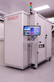
Aixtron launch CVD equipment for production of graphene

[Graphen Flagship News, LINK] From prototypes to products: AIXTRON's new systems enable cost-effective and large-scale production of graphene and related materials by chemical vapour deposition. Today, Graphene Flagship industrial partner AIXTRON showcased two new systems that enable cost-effective graphene production for a myriad of applications – such as consumer electronics, sensors, and photonics.The new devices allow the production of graphene under ambient conditions, and bring the cost of graphene films down by two orders of magnitude. 

The Neutron is a roll-to-roll system capable of depositing large areas of graphene on metal foils under ambient conditions (Photo: EU Graphene Flagship)


Graphene Flagship partner AIXTRON introduced results from two of its systems that enable the large-scale production of graphene through chemical vapour deposition (CVD). The Neutron is a roll-to-roll system capable of depositing large areas of graphene on metal foils under ambient conditions; and the CCS 2D system enables wafer-scale production of graphene on insulating wafers, a breakthrough that will speed up the development of new graphene electronics. To demonstrate the cost-effective nature of the graphene produced, AIXTRON distributed samples at the Industrial Forum.


The innovative Neutron system has a capacity of up to 20,000 square meters of graphene per year; this is around 200 times the production capacity of typical reactors in use today. Alex Jouvray, Programme Manager at AIXTRON and Graphene Flagship Work Package Leader for Production, explains that "Neutron is the product that resulted from of over three years of R&D, which included the demonstration of roll-to-roll graphene growth during the first stages of the Graphene Flagship project." Neutron brings the production of large areas of graphene beyond academic circles and to the factory floor. "The foil that is coated with graphene enters and exits the Neutron system under ambient conditions," explains Jouvray. "Since it doesn't need a vacuum, the Neutron can be easily placed inline at graphene manufacturing plants," he adds. Large-area monolayer graphene produced using this novel technique could lead to applications in transparent conductors, wearable devices, and coatings. "Moreover, it's economical," adds Jouvray. "With Neutron, we are able to bring the cost of a square meter of graphene CVD films down by two orders of magnitude," he explains. "It's a game-changer."

The versatile CCS system targets semiconductor applications. Here, there are stringent contamination requirements; usually, graphene needs to be grown on metallic surfaces and foils, which, being non-flat, are challenging to handle in the semiconductor industry and contain metal contamination that require further cleaning steps before the material can enter a fab. During the first years of the Graphene Flagship project, together with the group of Camilla Coletti at Graphene Flagship partner Istituto Italiano di Tecnologia (IIT), AIXTRON scaled the growth of graphene on insulators to full wafer-scale on its CCS 2D reactor, which can accommodate 2-inch up to 8-inch wafers. The wafers exhibit low contamination levels that meet the requirements of semiconductor fabs directly after growth. Camilla Coletti comments that "such tremendous progress is only possible thanks to the Graphene Flagship project which brings together top scientists from academia and engineers from a world-leading equipment company." The system is also capable of large-scale production of other layered materials, such as boron nitride or transition metal dichalcogenides.

Kari Hjelt, Head of Innovation of the Graphene Flagship believes that "these systems developed by AIXTRON show how our investment into prototypes during the first years of the Graphene Flagship are leading to products that enable mass production of graphene by chemical vapour deposition." He adds, "these discoveries open up thousands of possibilities beyond graphene, the arrival of wafers featuring other layered materials, or even 'sandwich' heterostructures are just around the corner," concludes Hjelt.

Andrea C. Ferrari, Science and Technology Officer of the Graphene Flagship and Chair of its Management Panel added that "the ultimate aim of the Graphene Flagship is to bring graphene and related layered materials from the lab to the factory floor. To take these new materials to the traditional semiconductor fabs, which is key to achieve their widespread application in consumer electronics, photonics and sensors, industrial tools capable of large area, large rate and low-cost manufacturing of graphene and related materials are needed.""With these systems," —adds Ferrari— "Graphene Flagship Partner AIXTRON leads the way fostering the new market opportunities that these new materials open. The ability to produce large scale graphene viably is of particular importance as the Graphene Flagship gears up to launch the first Graphene Foundry. Moreover, these products are a cornerstone in the innovation and technology roadmap of the Graphene Flagship, and shows that we are set to achieve the ambitious goals for our first ten years."

Wednesday, May 8, 2019

4th CMC Conference Enabled Critical Information and Connections

Fab materials event in Albany, New York area April 25-26 featured GlobalFoundries keynote and Intel and TI presentations. Plan now for the 2020 April 23-24 event in Hillsboro, Oregon. 

(SAN DIEGO (PRWEB) May 07, 2019) Over 150 leading executives and managers within the semiconductor manufacturing ecosystem gathered on April 25th and 26th in the Albany area of New York state for an important event on fabrication (fab) materials. The fourth-annual Critical Materials Council (CMC) Conference, produced by TECHCET, included topical presentations, a fab tour, exhibits by specialty materials suppliers, and networking roundtable discussions to learn about best-practices in a pre-competitive environment. Folks who missed attending the event this year can register to access the posted presentations for a nominal fee at https://cmcfabs.org/cmc-conference-2019/.

The event opened again, as in each of the prior three years, on an extremely strong business and technology keynote address by an executive from one of the CMC Fab member companies. The 2019 CMC Conference keynote was given by Dr. John Pellerin, Deputy CTO and VP of Worldwide R&D, GlobalFoundries. Pellerin talked about how demand for new high-volume manufacturing (HVM) semiconductor devices over the next few years will drive needs for increased numbers of new specialty materials as well as volumes of existing materials in his presentation on "Materials Challenges & Opportunities in Differentiated Technologies."

In the first session of the event covering global supply-chain issues of economics and regulations, G. Dan Hutcheson, CEO of VLSI Research, presented on "Slowdown: When did it start? What drove it? And When will the recovery come?" Hutcheson showed data from leading economic indicators that the recent decline in global semiconductor fab industry revenues due to memory chip prices may have already turned around.

TECHCET Sr. Analysts Dr. Jonas Sundqvist and Terry Francis presented updated information on demand drivers and forecasts for ALD/CVD precursors and Rare Earths, respectively. Sundqvist--also leader of the Thin Film Technologies Group at Fraunhofer IKTS--focused on how new 3D memory and logic chips demand more deposition precursors such that chemical volume growth will outpace that of silicon wafers, shown in the Figure. Francis showed how "Rare Earth" elements are not so rare at the elemental level, but complex dynamics between mining and refining and capitalism have led to a situation where mainland China currently controls most of the market for elements such as lanthanum (used in advanced ICs to create CMOS logic gates). Deep dives into all such materials matters are found in the TECHCET Critical Materials Reports (CMR), and you can find all of them online at https://techcet.com/shop/

Global semiconductor silicon quarterly wafer shipments 2015-2019 in millions of square inches (MSI). (Source: TECHCET)
The 2020 spring CMC Conference is scheduled for April 24-25 in Hillsboro, Oregon. The CMC Fab members and Associate members will again gather for two days of private face-to-face meetings before attending the public CMC Conference.

In addition to the annual spring CMC Conference in the US, there is also an annual fall CMC Seminar in Asia. The 2019 CMC Seminar will be held on October 17 in Taoyuan, Taiwan. For more information on CMC events see https://techcet.com/cmc-events/.

About CMC:
The Critical Materials Council (CMC) of Semiconductor Fabricators (CMCFabs.org) is a membership-based organization that works to anticipate and solve critical materials issues in a pre-competitive environment. The CMC is a business unit of TECHCET, and includes materials supplier Associate Members.

About TECHCET:
TECHCET CA LLC is an advisory services firm focused on process materials supply-chains, electronic materials business, and materials market analysis for the semiconductor, display, solar/PV, and LED industries. Since 2000, the company has been responsible for producing the SEMATECH Critical Material Reports™, covering silicon wafers, semiconductor gases, wet chemicals, CMP consumables, Photoresists, and ALD/CVD Precursors. For additional information about reports, market briefings, CMC membership, or custom consulting please contact info(at)cmcfabs(dot)org, +1-480-332-8336, or go to http://www.techcet.com or http://www.cmcfabs.org.

Wednesday, April 10, 2019

Strem high purity liquid ruthenium precursor for emerging ALD and CVD applications

Ruthenium has been under investigation for years among researchers all across the globe for applications such as high-work function electrodes in dynamic random access memory (DRAM) capacitors or gate stack in p-channel metal oxide semiconductor (MOS) in the front end of line (FEOL). It has also been considered for alloyed diffusion barriers, adhesion layers or seed layers in interconnects or through silicon vias (TSVs) for direct electrochemical deposition of copper in the back end of line (BEOL). In these applications, atomic layer deposition based on ultra-thin Ru films offer unique advantages.

Most of the available Ru ALD or CVD precursors have issues concerning low vapor pressure and high impurity levels, such as carbon and oxygen, which get incorporated in the films. In addition to that, long incubation times impacting throughput and process controllability, poor film adherence, and non-uniformity in high-aspect-ratio structures are some critical limitations of the field. However, Strem Chemicals—a high purity specialty chemicals’ manufacturer and supplier—offers a well-preferred bis(ethylcyclopentadienyl)ruthenium(II) [[(CH3CH2)C5H4]2Ru] (catalog number 44-0040) precursor for depositing Ru based ALD/CVD films for niche applications, such as aligned RuO2 nanorods. The pale yellow liquid precursor with a density of 1.3412 and vapor pressure ~0.2mm (85°C), is sold pre-packed in ALD cylinders by Strem Chemical. These fit many of the ALD tools on the market as well as many custom laboratory designed tools. 
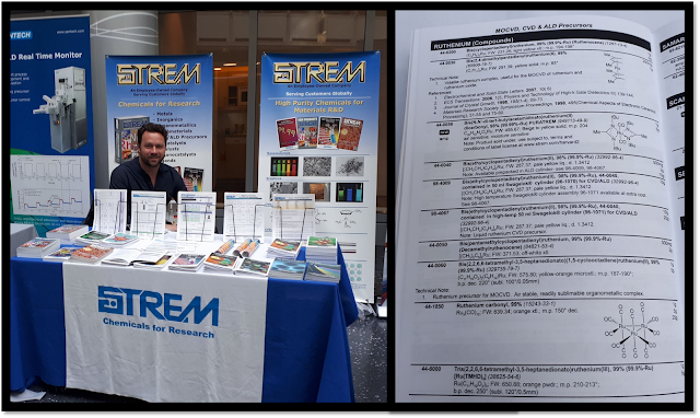
Recently, (March 19-20, 2019) Strem exhibited at the annual EFDS ALD for Industry Workshop in Berlin, Germany and we had a chance to discuss Ruthenium precursors with attendees. Here is a short section from the well-known Strem ALD/CVD Precursor Catalogue.

Here are just a few examples of thermal as well as plasma driven thin film deposition processes based on bis(ethylcyclopentadienyl)ruthenium(II) precursor presented by the diverse group of researchers at this meeting.

Thomas Waechtler et. al. have reported plating results on layers of ALD Cu with underlying Ru deposited using bis(ethylcyclopentadienyl)ruthenium(II) outperforming ones achieved on PVD Cu seed layers with respect to morphology and resistivity. Application of these processes suggest that a combination of ALD Cu with PVD or ALD-grown Ru could significantly improve the ECD Cu growth.
Researchers from the National Taiwan University of Science and Technology studied structures and electrochemical capacitive properties of RuO2 vertical nanorods encased in hydrous RuO2. They grew vertically aligned RuO2 nanorods with an aspect ratio in the range of 28-30 on the LiNbO3(100) substrate via metal-organic CVD (MOCVD) using bis(ethylcyclopentadienyl)Ru from Strem Chemicals. (Link)

A Korean research group has also reported plasma-enhanced ALD of Ru thin films performed using an alternate supply of bis(ethylcyclopentadienyl)ruthenium and NH3 plasma, where NH3 plasma acted as an effective reducing agent for bis(ethylcyclopentadienyl)ruthenium. The process exhibited no carbon or nitrogen impurities in the film as determined by elastic recoil detection time of flight analysis and the film density was found to be higher than that found in conventional oxygen based ALD.

Since 1964, Strem Chemicals, Inc. has been serving its clients from academic, industrial and government research and development laboratories as well as commercial scale businesses in the pharmaceutical, microelectronic and chemical/petrochemical industries. Strem (Headquarters: Newburyport, Massachusetts, USA) is a high quality specialty chemicals’ manufacturer and supplier. Strem also provides custom synthesis (including high-pressure synthesis) and current good manufacturing practice (cGMP) services. With ISO 9001 certification as a Quality Management System (QMS) standard with documentation, most of Strem’s products are reliable and of high purity, typically 99%, with some having 99.9999% metals purity. Strem utilizes a comprehensive range of analytical techniques tailored and applied to each product to ensure quality because the researchers typically rely on a supplier's quality procedures and documentation, which if poorly conducted may kill a great research idea. All of Strem's catalogs, since inception, have listed “Color and Form” for every product as a primary indicator of quality.

More than fifty years of experience in manufacturing inorganic and organometallic chemicals has enabled Strem to expand its product offering of MOCVD, CVD, and ALD precursors to continually add new products in support of this dynamic and exciting field. Strem’s CVD & ALD product range includes:

---
Promotional Blog for Strem Chemicals, Inc.
Researched, produced & written by BALD Engineering AB, Stockholm, 2019-04-10
Abhishekkumar Thakur, Jonas Sundqvist
www.baldengineering.com

In 2-Weeks: 2019 CMC Conference Highlights ALD/CVD Market and Technology Trends


In 2-Weeks: 2019 CMC Conference Highlights ALD/CVD  Market and Technology Trends 

 The upcoming CMC Conference, April 25-26, in Saratoga Springs, New York, will feature the latest forecasts on market drivers, trade issues, and technical issues facing precursors and other global materials supply-chains.  As shown below, CAGR for metal precursors is expected to exceed 11% through 2021.  Technology and Market Trends on atomic layer deposition (ALD) and chemical vapor deposition (CVD) precursors for IC fabs will be presented and discussed at this year's conference.

The Emerging Session will include: 
  • Dr. Jonas Sundqvist, Sr. Technology Analyst of TECHCET and Group Leader of Fraunhofer Institute will be revealing TECHCET's "Market and Technology Trend Forecasts for ALD & CVD Metal and Dielectric Precursors." (Sample shown below.) 
  • Dr. Matthew Stephens, VP of Sales and Product Management for Air Liquide, will provide a presentation on "Economic Considerations of ALD Precursor Selection."
  • Dr. David Thompson, Managing Director of Chemistry for Applied Materials, will present on "Preparing Supply-Chains and Managing Risk for an Uncertain Future on Emerging Devices."
  

Deputy CTO & VP of Worldwide R&D, GlobalFoundries  
 "Materials Challenges & Opportunities in Differentiated Technologies" 

 
3-Dynamic Sessions:
  1. Global Materials Supply-Chain and Market Issues
  2. Immediate challenges of materials & manufacturing 
  3. Emerging materials in R&D and pilot fabrication
Register now by clicking on the links, above, or go to: https://cmcfabs.org/cmc-conference-2019/

The public CMC Conference follows private CMC face-to-face meetings to be held April 23-24, 2019 at GlobalFoundries in Malta, New York.

Look Who's Coming - leading fabs, equipment & materials companies:
·        Samsung
·        Texas Instruments
·        GlobalFoundries
·        TowerJazz Panasonic
·        KFMI
·        Fraunhofer
·        Wonik
·        Ereztech
·        Matheson/TNSC
·        Linde
·        Inpria
·        IMEC
·        VLSI Research
·        SACHEM
·        Niacet
·        Grikin
·        Aveni
·        Silar Labs
·        ATI Metals
·        Momentive
 
·  STMicroelectronics
·  ON Semiconductor
·  Broadcom
·  TEL Technology Cntr
·  Umicore
·  Kinik
·  Revera/Nova
·  TECHCET
·  Strem Chemicals
·  Grikin
·  ATI Metals
·  Cryoin
·  MGC Pure Chemicals
·  Electronic Fluorocarbons
·  ShinHao Materials
·  Applied Seals
·  Peroxychem
·  Messer
·  MPD Chemicals
·  Mott Filters

·        Intel
·        Micron
·        Cypress
·        3M
·        IBM
·        Entegris
·        Air Liquide
·        Versum Materials
·        Air Products
·        Greene Tweed
·        Eastman
·        GrandiT
·        Edwards Vacuum
·        Mega Fluid Systems
·        Zing Semiconductor
·        Schrodinger
·        Boulder Scientific
·        Johnson Matthey
·        Veeco
·        ...and More!

2019 CMC Conference Sponsors: