Sunday, August 16, 2015

HERALD Workshop - ALD for Batteries, Gent, Belgium September 15-16

Workshop - ALD for Batteries

Co-organiser 

 cost logoHerald

Program

Tuesday, September 15, 2015 - Het Pand
09:30   Registration
10:00   Philippe Vereecken, IMECInvited Talk - Conformal deposition for 3D thin-film batteries: requirements and opportunities
10:45   Sebastien Moitzheim, IMECSpatial ALD of TiO2 for 3D thin-film batteries
11:15   Felix Mattelaer, Ghent University
ALD of Manganese oxides
11:45   Mikko Ritala, University of HelsinkiPreparation of lithium containing ternary oxides by solid state reaction of atomic layer deposited thin films
12:15   Lunch
13:30   Maarit Karppinen, Aalto University
Invited Talk 
14:15   Kevin van de Kerckhove, Ghent University
Molecular Layer Deposition of Titanicone
14:45   Miia Mäntymäki, University of Helsinki
15:15   Break
15:45   Adriana Creatore, TU Eindhoven
Invited Talk - Plasma ALD of Li-based materials
16:30   Thomas Dobbelaere, Ghent University
ALD of phosphates
17:00   Closing remarks

Wednesday, September 16, 2015 - Dept. Solid State Sciences

09:00   Ola Nilsen, University of Oslo
Invited Talk - ALD of Li-containing compounds
09:45   Amund Ruud, University of Oslo
High rate iron phosphates by ALD
10:15   Break
10:45   Ruud Van Ommen, TU Delft
ALD on battery particles
11:30   Geert Rampelberg, Ghent University
Thermal and plasma enhanced ALD on powders
12:00   Lunch
13:30   Tour of the Lab 

Registration

Participation is free of charge (limited number of places):https://webapps.ugent.be/eventManager/events/cocoonworkshopbatteries
Registration will be possible from 1 July 2015. Please register before 1 September 2015. 

Location

The workshop takes place at Het Pand (on Tuesday) and the department of Solid State Sciences (on Wednesday).

Tuesday, September 15, 2015

Het Pand, Ghent University
Onderbergen 1
9000 Gent, Belgium
By public transport:
  • From station Gent Sint-Pieters:Tram 1 (every 6 minutes) or tram 24 (every 20 minutes). Exit at Korenmarkt.
  • From Gent ZuidTram 4 (every 6 minutes), tram 24 (every 20 minutes) or bus 17 (every 30 minutes). Exit at Korenmarkt.
By Car:
  • Follow the parking signage to parking P7 Sint-Michiels. The parking is located at 50 meter from Het Pand. Take the exit Onderbergen and you come out in the wilderoosstraat, opposite Het Pand.
  • An alternative parking is P8 Ramen. From here it's about 5 minutes on foot to Het Pand.

Wednesday, September 16, 2015

Department of Solid State Sciences, Ghent University
Krijgslaan 281 - Building S1
9000 Gent, Belgium

Contact

Department of Solid State Sciences, Ghent University
Krijgslaan 281 - Building S1
9000 Gent, Belgium
Phone: +32 (0)9 264 43 54
Fax: +32 (0)9 264 49 96

Flyer

Sponsors

 iwt logo
FWO


Saturday, August 15, 2015

Nantero closes additional funding this summer for NRAM and adds ex TSMC Executive to the Board

I have noticed that Carbon Nanotube integration into semiconductor processing as an active device or sensor material has moved into a more mature phase lately. One example is the company Nantero who earlier this summer announced closing a $31.5 million Series E financing round from new and existing investors now adds Previous TSMC Executive Dr. Shang-Yi Chiang to its Advisory Board


According to the press relase Dr. Chiang was previously an Executive Vice President, Co-Chief Operating Officer and Senior Vice President of R&D at TSMC before announcing his retirement in October 2013. 


NRAM is based on forming a film of Carbon Nanotubes (CNT) that are deposited onto a standard silicon substrate that contains an underlying cell select device and array lines (typically transistors or diodes) that interface the NRAM switch. The NRAM acts as a resistive non-volatile random access memory NVRAM and can be placed in two or more resistive modes depending on the resistive state of the CNT fabric. When the CNTs are not in contact the resistance state of the fabric is high and represents a “0” state (see Figure below). When the CNTs are brought into contact, the resistance state of the fabric is low and represents a “1” state. (www.nantero.com)


“Nantero continues to attract the industry’s brightest and most innovative minds both internally and on an advisory basis,” said Greg Schmergel, Co-Founder, CEO and President of Nantero. “This added expertise will be instrumental in helping the company deliver a new generation of memory with the unique properties of DRAM-like speed, nonvolatility, and ultra-high-densities, for both standalone and embedded use.”


Additional information at the www.nantero.com  tells us: NRAM can enable a variety of exciting new features and products in both consumer and enterprise electronics. This new super-fast, ultra-high density memory can replace both DRAM and flash in a single chip, or enable new applications as a storage class memory, while also delivering the low power, high speed, reliability, and endurance needed to drive the next wave of electronics innovation.

  • NRAM Advantages: Extremely Low Power, Super-Fast, High Density, High Endurance
  • Limitless Scalability: Can Scale Below 5 nm to Enable Terabits of Memory in the Future
  • Proven Technology: Successfully Used in Mass Production CMOS Fabs for Many Years
  • Exciting Future Products: Virtual Screens, Next-Generation Enterprise Systems, Rolled-up Tablets, Instant-On Laptops, 3D Video Phones and other products needing huge amounts of fast memory
Here is also a video where the founders of Nantero tells us more about the revolutionary emerging memory technology they are commercializing - claiming scaling down to 5 nm and "unlimited storage capacity" for our future electronic gizmos.
 

Zinc oxide ALD coated alpha-phase ferric oxide particles for water purification

Zinc oxide-coated alpha-phase ferric oxide particles can be used for water purification purposes. This has been demonstrated by Giuliana Impellizzeri and co-workers CNR-IMM (Institute for Microelectronics and Microsystems) Catania, Italy, using a a Picosun R-200 advanced atomic layer deposition (ALD) system to deposit polycrystalline ZnO on alpha-phase ferric oxide (α-Fe2O3) nanoparticles (which were purchased from Sigma-Aldrich).


(a) Transmission electron microscopy images of zinc oxide-coated ferric oxide (Fe2O3) core-shell nanostructures. (b) High magnification image of a single core-shell nanoparticle. (c) High magnification image of a single uncoated Fe2O3nanoparticle. (13 August 2015, SPIE Newsroom. DOI: 10.1117/2.1201508.006078)

Core-shell nanostructures with promising photocatalytic characteristics

Giuliana Impellizzeri, Alessandro Di Mauro, Guillaume Amiard, Simona Boninelli and Vittorio Privitera


One of the most pervasive problems afflicting people today is inadequate access to clean water and sanitation. By 2030—as estimated by the United Nations—47% of the world's population will live in areas with high ‘water stress’ levels. Removing pathogens, chemicals, and other contaminants to produce satisfactory water supplies (i.e., with high throughput and at a low cost) is thus a growing challenge around the world. It is thought, however, that nanotechnology can be used to improve water purification techniques. It should also be possible to reduce the cost of prohibitively expensive water cleaning methods, which are currently unaffordable for many developing countries

Thursday, August 13, 2015

UPDATE: Symposium of the ALD Lab Dresden at SEMICON Europa October 6


Workshop on Atomic Layer Processing

Date: 6 October 2015
Time: 09:00 - 15:10
Location: Room Columbus, Messe Dresden
 
Organized by:

Looking back in the evolution of IC technology, it can be stated that from the 0.25µm node on, the key for further shrinking was planarization. This was enabled by the introduction of an emerging technology, the CMP. Since the 28 nm node it can be observed that, at least in the front end of line, starting with the FinFET and possibly continuing with the surrounding gate transistor, the required structures become more and more three dimensional, while the thickness of the associated films become extremely thin (gate dielectric, work function layer, barrier layer). The emerging technology enabling this is Atomic Layer Deposition (ALD).

Dresden am Abend mit Dresden Fotografie, I love Dresden und Unser Sachsen (Facebook, by Jens Heike)


ALD is based on self limiting heterogeneous chemical reactions which allow the fabrication of very thin (sub nm to few nm) layers with high accuracy (basically atomic layer precision), extremely well conformality and intrinsically high uniformity even in batch tools. Although the scientific background of ALD goes far back in history, ALD for semiconductor processing can still be considered as a novel technology. 

Progress in ALD is associated with tools, but even more with specifically designed precursors which need to be applied at optimum conditions of the gas feed system, the process chamber and the substrate condition. Our workshop, which is organized by the “ALD Lab Dresden” wants to stimulate discussions between developers of tools, consumables, as well as applicants of this exciting technology.

The self limiting behavior of the heterogeneous reaction can however also be used to remove material from a substrate in an extremely controlled fashion of atomic dimensions. This process, that can be viewed as the complement to ALD is called Atomic Layer Etching (ALEt). As for ALD also ALEt can be a game changer for the semiconductor industry utilizing surface functionalization and modification similar to those we know in ALD and resulting in a chemistry-based material removal on the same atomic level as in ALD – A layer by layer removal. 

In general scaling is thought about to be a shrink in the critical dimensions (CD, pitch) in the latheral xy-plane, today scaling is also taking place in the z-direction, i.e.,  a reduction in the thickness of the film stacks like the High-k Metal Gate stack. This has resulted in that the thicknesses of the film stacks of devices today are now routinely approaching <20 Å nm providing an opportunity for slow and precise etching by ALEt.

We hope that this new part of the ALD Lab Dresden Symposium will allow for increased scientific and technological discussion for enabling ALEt and learning from ALD and related plasma based processing techniques like Plasma CVD and Reactive Ion Etching.
 

AGENDA


09:00WelcomeOrganized by:


Supported by:

cost logo


Prof. Johann W. Bartha, TU Dresden
 
09:15In situ monitoring of Atomic Layer Deposition in porous materials
Martin Knaut, TU Dresden
 
09:40Passivation of MEMS by Atomic Layer Deposition
Matthias Schwille, Robert Bosch
 
10:05TBD
Colin Georgi, TU Chemnitz/FhG ENAS
 
10:30TBD
Stefan Riedel / Sascha Bönhardt, FhG IPMS-CNT
 
10:55ALD coatings for applications as permeation barrier and protective layer in fiber-reinforced materials
 Mario Krug, FhG IKTS
 
11:20ALD for solar cell application
 Ingo Dirnstorfer, NaMLab
 
11:45Plasma enhanced ALD process for TiO2- and WO3- films
Alexander Strobel, FH Zwickau
 
12:10Lunch Break (Conversation, Networking, Finger food)
 
13:00Atomic Layer Etching
Jonas Sundqvist, Lund University
 
13:25Spatial Atomic Layer Deposition and Atomic Layer Etching
Prof. Fred Roozeboom, TU Eindhoven
 
13:50Atomic Layer Etching: What Can We Learn from Atomic Layer Deposition?
Harm Knoops, Oxford Instruments/TU Eindhoven
 
14:15TBD
Stephan Wege, Plasway
 
14:40Industrial High Throughput Atomic Layer Deposition Equipment and Process for OLED Encapsulation
Jacques Kools, Encapsulix
 
15:05Closing Remarks / Wrap Up
Prof. Johann W. Bartha, TU Dresden
 
15:10End
 

Registration

No pre-registration required but you must register as a visitor, in order to gain access to the venue:
 

Wednesday, August 12, 2015

Demand for 200 mm tools outstrips supply according to Applied Materials

According to David Lammers at Applied Materials (Nanochip COVER STORY: DEMAND FOR 200MM TOOLS OUTSTRIPS SUPPLY).

This must be a good opportunity for the ALD suppliers like Picosun, Oxford Instruments, BENEQ and Ultratech CNT to get into the game and supply ALD chambers for all kinds of More than Gordon Moore applications like MEMS, Capacitors and other devices and single layer applications. As far as I know you can´t buy new ASM Pulsar 200 mm chambers anymore so have to get a 300mm bridge tool and the other options you have are for sure 200 mm large batch furnaces from ASM or Tokyo Electron but those have cycle time penalty and high thermal budget and none of these have PEALD capability, which as reported here many times is booming in scientific activity and possibly also in production.


A wide variety of systems, ranging from smartphones and autos to wearables, rely on trailing-edge devices made on 200mm wafers. (Source: Applied Materials)


TSMC and its joint ventures own the most 200mm wafer fab capacity, while STMicroelectronics, a power in the MEMS sensor field, is the leading 150mm wafer processor. (Source: IC Insights)

Just to refresh everybody's memory, eher is a table summarizing many of those alternatives for 200 mm ALD suppliers published by ALDPulse some time ago.


Ultratech Cambridge NanoTech announced that the 1000th paper using one of their ALD tools

I previously posted this paper (here) and it turns out that this is as announced today by Ultratech Cambridge NanoTech, the 1000th peer-reviewed paper written on its ALD systems was published in July 2015 inChemistry of Materials


The paper entitled "Atomic Layer Deposition of the Solid Electrolyte LiPON" was authored by Alexander Kozen, Ph.D, a member of the Nanostructures for Electrical Energy Storage (NEES) group at the University of Maryland. This milestone figure underscores the fact that today, almost one-fifth of the total peer-reviewed ALD publications worldwide, since the founding of the company in 2003, have been written based on using Ultratech-CNT systems (based on Web of Science analysis). 


University of Maryland Professor and principal investigator at the Energy Frontier Research Center (EFRC) Gary Rubloff said, "The performance and flexibility of our Ultratech Fiji systems have driven our group's nano research since 2011. The role played by these systems has been critical in many of the advances made in Nanostructures for Electrical Energy Storage (NEES)--our DOE, Energy Frontier Research Center. The research undertaken has involved a variety of collaborations across the Center to exploit ALD films as cathode, anode, current collector, solid electrolyte, and passivation/stabilization layers distributed as highly conformal, high quality layers on 3-D structures in the most demanding nano-geometries. As part of our most recent work, we have just developed the first reported ALD process for lithium phosphorous oxy-nitride (LiPON), a well-known, solid-state electrolyte for safe batteries. Through the use of real-time, in-situ ellipsometry, the process was optimized in a systematic fashion. ALD allows us to grow very thin LiPON layers that we are applying to passivation of high-energy lithium anodes as well as to solid-state batteries."


Ultratech-CNT Vice President of Research and Engineering Ganesh Sundaram, Ph.D. said, "While the traditional gauge of system productivity has focused on metrics such as wafer output, we have chosen to concentrate on creating products which motivate and enable intellectual output. The 1000th paper milestone attests to the fact that the Ultratech-CNT ALD systems are at the forefront for generating high quality, and strongly-cited research in this fast growing field. Furthermore, the large library of research papers based on our systems also provides substantial benefits to new researchers entering the field as they will be able to take advantage of the solid foundation of published research that underpins these ALD systems."


Dr. Kozen is part of The Rubloff Group at the University of Maryland where Professor Gary Rubloff heads the Nanostructures for Electrical Energy Storage (NEES), Energy Frontier Research Center (EFRC), a program of the Department of Energy (DOE). The paper was published in Chemistry of Materials (DOI: 10.1021/acs.chemmater.5b01654).

BALD 2015 in Tartu LATE-NEWS ABSTRACT SUBMISSION FOR POSTER PRESENTATIONS.

LATE-NEWS ABSTRACT SUBMISSION FOR POSTER PRESENTATIONS.
We are pleased to announce that a limited number of late-news poster presentations  can be included into the program of the 13th International Baltic Conference on Atomic Layer Deposition. 


The abstract submission deadline is August 17, 2015.
Please find here the call for late-news abstracts.
Please use the online form below for uploading your abstract. Guidlines for formation of the abstract can be found from here. In addition to the abstract file all the graphics should be also uploaded separately via online form to ensure the good print quality.

Abstract submission rules:
  • Abstract must be submitted in word and pdf format, using the guidelines that can be found from here.
  • In order to ensure sufficient print quality, the figure(s) should be uploaded as separate files (TIFF for halftone images and PDF for line drawings) in addition to MS Word and PDF files of the abstract with embedded figure(s) and figure caption(s). File size 300-700KB.
  • One Abstract can include up to two pictures or graphics.
  • Up to two poster presentations per Full Registration can be accepted.
  • One Presentation per Student Registration can be accepted.

Rice U. discovery may boost ReRAM memory technology

My favorite high-k metal oxide Ta2O5 is used again for a resistive RAM memory - this time with my least favorite material - Grrrraphene. Just can´t stand the hype I guess. Anyhow considering recent developments in cross bar Memory cell technology by Intel and Micron this could prove to be a future prospect.


A schematic shows the layered structure of tantalum oxide, multilayer graphene and platinum used for a new type of memory developed at Rice University. The memory device overcomes crosstalk problems that cause read errors in other devices. 
(Tour Group/Rice University)

PUBLIC RELEASE: 10-AUG-2015Rice U. discovery may boost memory technology
Rice University scientists make tantalum oxide practical for high-density devices


Scientists at Rice University have created a solid-state memory technology that allows for high-density storage with a minimum incidence of computer errors.

The memories are based on tantalum oxide, a common insulator in electronics. Applying voltage to a 250-nanometer-thick sandwich of graphene, tantalum, nanoporous tantalum oxide and platinum creates addressable bits where the layers meet. Control voltages that shift oxygen ions and vacancies switch the bits between ones and zeroes.

The discovery by the Rice lab of chemist James Tour could allow for crossbar array memories that store up to 162 gigabits, much higher than other oxide-based memory systems under investigation by scientists. (Eight bits equal one byte; a 162-gigabit unit would store about 20 gigabytes of information.)

Details appear online in the American Chemical Society journal Nano Letters. More details can be found here: http://www.eurekalert.org/pub_releases/2015-08/ru-rud081015.php

Applications Engineer - ALD at Oxford Instruments’ Plasma Technology

Applications Engineer - ALD, Yatton, Bristol


Oxford Instruments’ Plasma Technology business is looking for an Applications Engineer to play a key role in the Atomic Layer Deposition (ALD) team by developing processes within design boundaries and timescales. In this role you will process and demonstrate customer samples, liaise with customers, support system acceptances and provide customer training both in the UK and overseas. Ideally you will have a background in chemistry and experience of the semiconductor industry, and/or chemical engineering experience.

The Role

Key responsibilities of the role will include (but not be limited to):
  • To push the performance boundaries of existing technology to process and demonstrate samples. 
  • To contribute to the process development for the ALD project. Liaise with all members of the project team and interpret their requirements into sample processing requirements.
  • Analyse the results of the test samples and produce technical reports.
  • Develop an excellent working knowledge of the technology to facilitate fault finding and root cause analysis on processing results or equipment performance.
  • Carry out customer training both at Plasma Technology and at customer sites.

The Person

A relevant science or engineering degree. Chemistry or Chemical engineering would be an advantage. Ideally, experience of the semiconductor industry and/or chemical engineering experience. Exposure to atomic layer deposition or reactive ion/high density plasma etching processes an advantage.
  • Nanotechnology measuring skills (e.g. SEMS, Nanospecs, Ellipsometry).
  • MOCVD (metal organic chemical vapour deposition).
  • PECVD (plasma enhanced chemical vapour deposition).
  • ALD (atomic layer deposition).
  • Self-starting, diligent and enthusiastic. A professional approach to working independently and managing your own time.
  • Highly innovative and good lateral thinking skills.
  • Focused on excellent customer service.
  • Good diagnostic skills and problem solving abilities. Positive and enthusiastic attitude to technical challenges, and flexibility to cope effectively with changes to specifications or priorities.
  • Excellent written and oral communication. Able to articulate, present and report on technical or complex issues clearly and succinctly.

Business Overview

Oxford Instruments Plasma Technology provides a range of high performance, flexible tools to semiconductor processing customers involved in research and development, and production. Oxford Instruments plc is a global company with manufacturing facilities, offices and service centres, worldwide.

To apply, please submit your CV to caroline.read@oxinst.com

www.oxford-instruments.com/businesses/nanotechnology/plasma-technology

Follow us at www.twitter.com/oxinst or www.facebook.com/oxinst

Note to recruitment agencies: Oxford Instruments does not accept agency CV’s. Please do not forward details to our jobs alias, Oxford Instruments employees or any other company location. Oxford Instruments is not responsible for any fees related to unsolicited CV’s

Monday, August 10, 2015

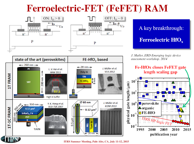
Ferroelectric HfO2 by ALD Key Breakthrough in ITRS “Beyond CMOS” Update 2015

Following the ITRS Summer Meeting, Palo Alto, CA, July 11-12, 2015 Ferroelectric HfO2 by Fraunofer CNT and NaMLab in Dresden Germany is showcased as a "Key Breakthrough" in the ITRS “Beyond CMOS” Update 2015. You can find this presentation in by ITRS Emerging Research Devices (ERD) amongst others in the excellent new ITRS 2.0 website : http://www.itrs2.net/


ALD listed as Top 10 Advanced Manufacturing and Automation Technologies

Research and Markets has announced the addition of the "2015 Top Technologies in Advanced Manufacturing and Automation" report to their offering and Atomic layer Deposition is up in the Top 10 among technologies like Advanced Lithography, Agile Robots and Magnetic Leviatation(!)


Top 10 Advanced Manufacturing and Automation Technologies - Deep Dive Analysis
  1. 3D Printing
  2. Multimaterial Joining Technologies
  3. Composites Manufacturing
  4. Atomic Layer Deposition
  5. Nanomanufacturing
  6. Digital Manufacturing
  7. Micromanufacturing
  8. Agile Robots
  9. Advanced Lithography
  10. Magnetic Levitation