Sunday, July 5, 2015

University of Wisconsin Madison demonstrate biodegradable microwave flexible TFTs

University of Wisconsin Madison demonstrate microwave flexible TFTs built on a cellulose nanofibrillated fiber (CNF) substrate by employing transferrable single crystalline Si nanomembranes (Si NMs)


(a) Illustration of the degradable  (b) Microscopic image of a finished device on the CNF substrate. (c) An optical image showing the transparency and flexibility of the CNF substrate. (d) An optical image and (e) an enlarged optical image showing the biodegradability of the array of devices built on the CNF substrate: (left) as-made and (right) after 3 weeks degradation.
Citation: Appl. Phys. Lett. 106, 262101 (2015); http://dx.doi.org/10.1063/1.4921077

Microwave flexible transistors on cellulose nanofibrillated fiber substrates


Jung-Hun Seo, Tzu-Hsuan Chang, Jaeseong Lee, Ronald Sabo, Weidong Zhou, Zhiyong Cai, Shaoqin Gong and Zhenqiang Ma

Appl. Phys. Lett. 106, 262101 (2015); http://dx.doi.org/10.1063/1.4921077

In this paper, we demonstrate microwave flexible thin-film transistors (TFTs) on biodegradablesubstrates towards potential green portable devices. The combination of cellulose nanofibrillated fiber (CNF) substrate, which is a biobased and biodegradable platform, with transferrable single crystalline Si nanomembrane (Si NM), enables the realization of truly biodegradable, flexible, and high performance devices. Double-gate flexible Si NM TFTs built on a CNF substrate have shown an electron mobility of 160 cm2/V·s and f T and f max of 4.9 GHz and 10.6 GHz, respectively. This demonstration proves the microwave frequency capability and, considering today's wide spread use of wireless devices, thus indicates the much wider utility of CNF substrates than that has been demonstrated before. The demonstration may also pave the way toward portable green devices that would generate less persistent waste and save more valuable resources.


Friday, July 3, 2015

UPDATED - 2014 PEALD Year in Review

The Plasma ALD Guy has updated his 2014 PEALD Year in Review : http://plasma-ald.com/2014YIR/2014YIR.php and republished below.

"To date, I have tracked down 131 publications using PEALD films accepted for publication during 2014. There are probably others I have not yet come across. Papers in which the focus is the development of PEALD films tend to be quite easy to track down. When PEALD is just one of the techniques utilized for some new application, finding the paper can be challenging, especially when few processing details are offered at which to point a search engine. Identifying these publications may be more challenging, but it is fun when I do find them and it is great to see the breadth of applications for which PEALD films are being utilized."

2014 PEALD Publications by Month

2014 PEALD Films

2014 PEALD Hardware

2014 PEALD Locations

Thursday, July 2, 2015

Picosun and Carleton Strike Gold with ALD


Picosun Oy, the leading provider of high quality Atomic Layer Deposition (ALD) solutions for industrial manufacturing, and Carleton University, Canada, report uniform ALD gold deposition on complete silicon wafers. The gold films were prepared using PICOSUN™ plasma ALD tool and a new gold precursor developed by Prof. Seán Barry. The novel process was described in the talk given at the AVS 15th ALD meeting held in Portland, USA.


Gold is a highly sought-after material in today's microelectronics, optoelectronics, and microsystems manufacturing. Due to its excellent chemical inertness and high thermal and electrical conductivity it has a plethora of applications for example in 3D packaging (via interconnects), wafer metallization, and heat dissipation of IC components, and preparation of electrical connections, structural layers, and electrodes for MEMS devices.

"We have worked on gold metal deposition chemistry for a few years now, and this process is a breakthrough. Our PICOSUN™ ALD system handles a wide variety of precursors beautifully, and its ease of use has made process development for challenging materials much easier. The uniformity that we are able to achieve with the PICOSUN™ plasma ALD tool is very impressive," states Seán Barry, Associate Professor of the Department of Chemistry, Carleton University, Ottawa, Canada.

"We are excited about these recent advances in gold deposition by ALD. Picosun's plasma ALD technology is optimal for metal deposition. This has enabled gold manufacturing also before, but the now published, larger scale results will definitely catch the interest of a vast number of our production customers in IC, MEMS, and electronics industries," summarizes Dr. Wei-Min Li, Applications Director of Picosun.

Picosun provides the most advanced ALD thin film technology and enables the industrial leap into the future by novel, cutting-edge coating solutions, with four decades of continuous expertise in the field. Today, PICOSUN™ ALD systems are in daily production use in numerous major industries around the world. Picosun is based in Finland, with subsidiaries in USA, China, Taiwan, and Singapore, and a world-wide sales and support network.

Located in the nation's capital, Carleton University is a dynamic research and teaching institution with a tradition of leading change. Its internationally recognized faculty, staff and researchers provide more than 27,000 full- and part-time students from every province and more than 100 countries around the world with academic opportunities. Carleton's creative, interdisciplinary and international approach to research has led to many significant discoveries and creative works in science and technology, business, governance, public policy and the arts. As an innovative institution, Carleton is uniquely committed to developing solutions to real-world problems.

Wednesday, July 1, 2015

Leading Edge Embedded NVM Workshop September 28-30 at Centre Microélectronique de Provence

The "Leading Edge Embedded NVM Workshop" (e-NVM), with the support of "l'Ecole Nationale Supérieur des Mines de Saint-Etienne", is organized by ARCSIS, a trade association for the microelectronics and semiconductor activities in the Provence-Alpes-Riviera (PACA) region, in France. ARCSIS participates in assuring sustainability, full economic development and enhanced competitiveness of the regional microelectronics and communicating objects industry.


Further to the success of the second edition of the «Leading-edge Embedded Non Volatile Memories» workshop in 2013 with over 180 international participants, ARCSIS reiterates the event in 2015 at the «Centre Microélectronique de Provence» in Gardanne (Aix-en-Provence area, France). The third edition of this workshop dedicated to embedded non-volatile memories takes place from 28 to 30 of September 2015.

The aim of the Workshop is to bring together researchers and industrials of both sides of the chain around Embedded Non-Volatile Memories: designers and manufacturers on the one hand and contractors and end-users on the other hand.

Worldwide specialists in research and industry of Embedded NVM domain have participated in e-NVM: Altis Semiconductor, Applied Materials, ASM International, ATMEL, CEA-LETI-MINATEC, CEA-Liten, Crocus Technology, Cypress Semiconductor, ELMOS Semiconductor AG, EMSE / CMP, EM Microelectronics (Swatch), Gemalto, Globalfoundries, Grace Semiconductor, IMEC, IM2NP Aix –Marseille University, Infineon Technologies AG, Inside Secure, Institut des Matériaux de Nantes, Institut Supérieur d’Electronique de Paris, LIRMM, Molecular Electronics Research Institute (MERI JSC), Nantero, NXP Semiconductors, Oerlikon Systems, Polytech’Nice, Rambus, Robert Bosch Gmbh, Samsung Electronics Co. Ltd, Starchip, STMicroelectronics, Università di Modena e Reggio Emilia, X-FAB Semiconductor Foundries AG...

Some companies and laboratories have already confirmed their participation as invited speakers: 

Aix-Marseille University-IM2NP (France) - Vincenzo Della Marca
CEA-LETI (France) - Bastien Giraud
CEA-Leti and IM2NP (France) - Alexandre Levisse
CEA, LETI, MINATEC Campus (France) - Gabriele Navarro
CEA-SACLAY (France) - Christian Gamrat
Crocus/LIRMM (France) - Sophiane Senni
Crossbar (USA) - Sylvain Dubois
Cypress Spansion (USA) - Igor Kouznetsov
Forschungszentrum Juelich GmbH (Germany) - Dr Vikas Rana
GLOBALFOUNDRIES Europe (Germany) - Robert Meier
Grace Semiconductor (China) - Weiran Kong
IM2NP (France) - Damien Deleruyelle
Inside Secure (France) - Laurent Sustek
Integrated System Solution Inc. (USA) - Julian Chang
Kilopass (USA) - André Hassan
Macronix (Taiwan) - Jocelyn Carroue
Panasonic (Japan) - Takumi Mikawa
Politecnico di Torino (Italy) - Elena Ioana Vatajelu
Rhealtys (France) - Jean-Pierre Delesse
Safran/Morpho (France) - Nicolas Prawitz
Samsung (Korea) - Jisung Kim
SMIC (China) - Jay Ning
SST-Microchip (USA) - Alex Kotov
SST-Microchip (USA) - Nhan Do
Starchip (France) - Speaker to be confirmed
STMicroelectronics – MMS Group (Italy) - Antonino Conte

Kurt J. Lesker introduces new R&D Platform for organic material deposition, ALD and PEALD

Kurt J.Lesker's most affordable organic material deposition system platform, designed specifically with the entry to mid-level user in mind. Standard configurations compatible with up to 100mm x 100mm square or 150mm diameter substrates, up to 350°C heating and cooling, glove box option available.


  • Designed to accommodate specific organic and inorganic thin film applications such as, OLED Displays, Lighting, Organic Photovoltaics and Electronics.
  • Offers both organic and metal deposition capabilities in a single chamber.
  • Recipe driven computer system control with data logging option available.
  • Field tested and proven design.

Glovebox Interfaced System: Incorporates a sliding front door with glove box interface flange and sliding rear door for unobstructed chamber access. Facilitates thermal and plasma enhanced atomic layer deposition techniques

Standard chambers are configured to allow up to:

(12) 1cc, 10cc, or 35cc plug-in low-temperature organic sources

(4) Thermal evaporation sources and pellet feeder option

- Personalised combinations available based on system platform

- Scroll type rough pumping; cryogenic high vacuum pumping

- Standard configurations compatible with up to 8" x 8" (200mm x 200mm) square substrates, up to 350°C heating, glove box, up to five mask storage shelves with motorised transfer, and wedge tool options

- Basic computer control with recipe and data logging options are available as well

Fraunhofer Center for Nanoelectronic Technologies Installs 200mm PEALD FlexAL Tool

The Fraunhofer IPMS  in Dresden, Germany has installed a FlexAL system for plasma enhanced and thermal ALD from Oxford Instruments Plasma Technology in its Center for Nanoelectronic Technologies.


The fields of use for the new tool are research and development on processes for metal oxides for ultra-thin integrated 3D capacitors, the development of new and unique metal ALD processes, and as a platform with a combinatorial screening concept including in-situ metrology and standardised tests for ALD/PEALD precursor development serving gas and chemical supplying companies. Additionally the FlexAL will serve as a 200mm PEALD tool for the MOEMS pilot line at the Fraunhofer IPMS.


The Center for Nanoelectronic Technologies has a long-term experience in atomic layer deposition (ALD), which is a sophisticated process where monolayer after monolayer is built up. ALD is the process of choice whenever precise thickness and composition control of thin films in the nanometer range are required. This is particularly the case for semiconductor devices where the smallest dimensions of some tens of nanometer are fabricated, and an increasing demand is observed for high conformal thin ALD films. Consequently, the development of materials and compounds deposited by ALD increases impressively.

After a rigid tendering process the Oxford Instruments FlexAL PEALD system was chosen because of its capabilities as a high end ALD research and development tool. The broad range of processes enabled by the FlexAL’s design allows the combination of plasma and thermal processes in one fully automated recipe as well as the flexible precursor cabinet which enables effective combinatorial precursor screening with in-situ metrology.

“The proven performance and versatility of the Oxford Instruments FlexAL together with the availability of multiple room temperature variants of PEALD processes made it the ‘system of choice’ for the Center for Nanoelectronic Technologies. We are extremely pleased to be supplying this prestigious research institute with this,” says Dr. David Haynes, Sales, Service and Marketing Director, Oxford Instruments Plasma Technology.

Sunday, June 28, 2015

ALD History reading to re-activate, more voluntary contributors welcome

The volunteer-based Virtual Project on the History of ALD (VPHA), launched about two years ago (AVS ALD 2013, San Diego), has already significantly advanced our understanding of the history of ALD. It has become clear that ALD has been invented twice independently of each other, under different names, at different times and geographical locations. 


The main VPHA activity, reading and commenting on early ALD works up to 1986, has so far resulted in three joint publications (see http://vph-ald.com/Publication%20Plan.html). It is getting time to complete the reading and create at least one more publication, aimed at the AVS ALD 2016 conference.

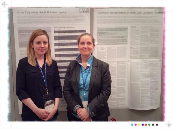
AVSALD 2014 #ALDep conference: the two #VPHA posters, with co-authors from Bilkent (Riikka, Twitter)


VPHA in numbers: 

* There are currently 325 ALD papers listed up to year 1986. 
* About 1000 comments to be given (at least three comments per paper). 
* 36 people from ten countries and >20 affiliations have already given comments in the ALD-history-evolving-file. 
* There is room for many more to join and contribute.


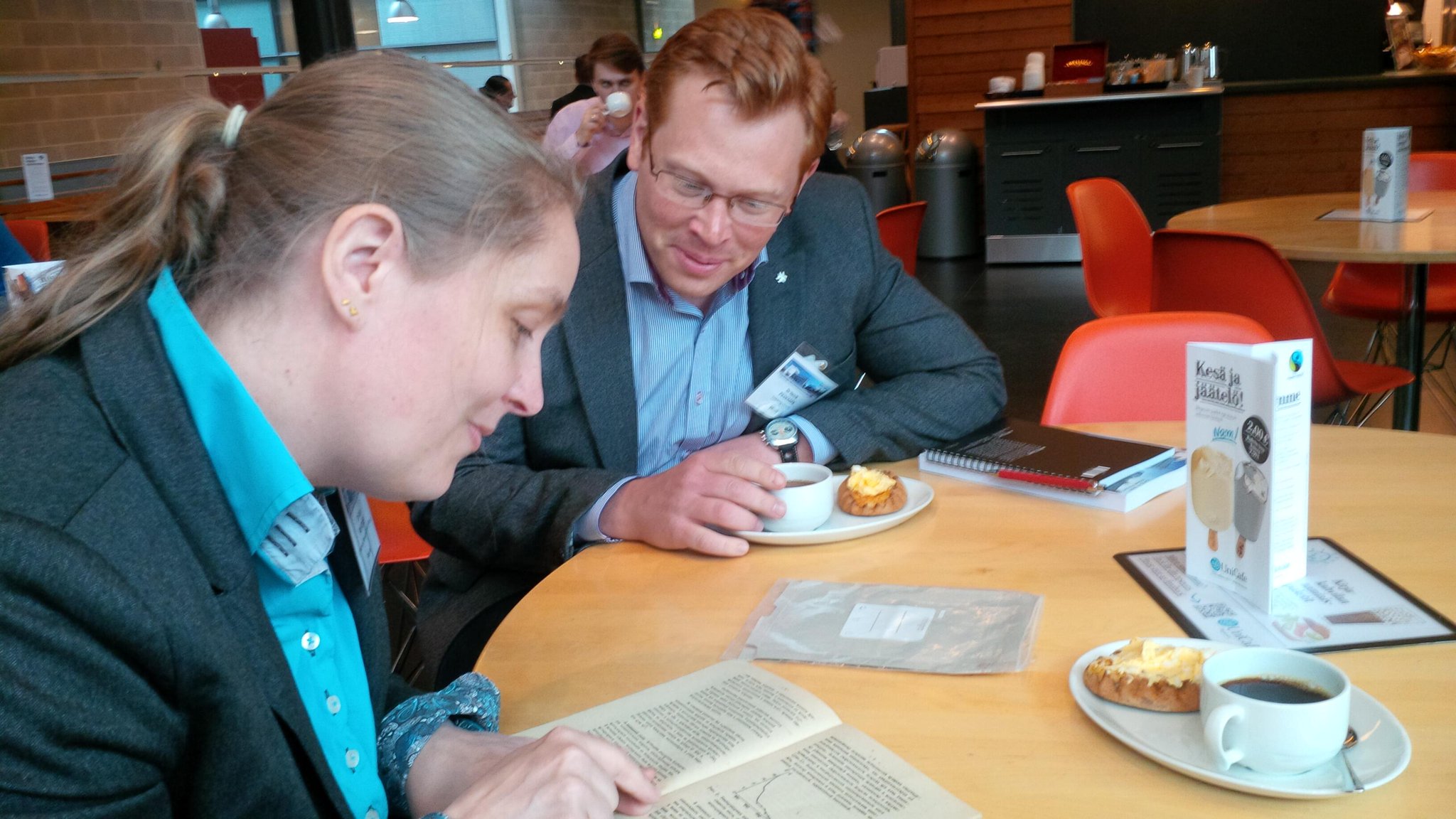
Baltic ALD 2014 in Helsinki: Eating Finnish Pirogs and reading Russian ALD papers looking for the first reference for HfO2 by ALD (Riikka and Henrik)

The condensed publication plan of VPHA is below; full publication details you find from the website created for the VPHA collaboration: http://vph-ald.com. There is also a LinkedIn group, with discussions related to the VPHA and other ALD history aspects:https://www.linkedin.com/groups/ALD-History-5072051/about


...and then the answer pointed out by Prof. Drozd himself.

If you are interested joining this unique international collaborative effort, we warmly welcome you on board. For an active start, you can directly add comments in the ALD-history-evolving-file. We are also in the process of creating a “workflow” which will guide one to read the articles that need it the most.


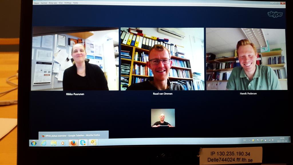
Skype call planning for the VPHA reading project (Riikka, Ruud, Henrik and Jonas)

Info on the progress of “the workflow” and other things will be shared in the ALD History LinkedIn group and through occasional emails to the VPHA authors and prospective authors. To join this VPHA email list, please send me (Riikka) a message - either reply to this post, send a LinkedIn message, or email riikka.puurunen@vtt.fi. 

Best regards, 
Riikka Puurunen, the (unofficial) VPHA coordinator 

--- 

1) Poster at Baltic ALD 2014 - done 
2) Poster at ALD 2014, Kyoto - done 
3) Presentation at ALD 2014, Kyoto - done 
4) ALD history tutorial at ALD 2014, Kyoto – done 
5) Essay on the early history of ALE-ALD – done 
6) Website for ALD history and VPHA – done, http://vph-ald.com
7) Exhibition: 40 years of ALD in Finland - Photos, Stories (FinALD40) – done 
8) Review article/essay on the early history of ML-ALD - ongoing 
9) Presentation at ALD 2016 - ONGOING 
10) Optional: general ALD history review article 
11) Updating wikipedia 
12) Closing the VPHA

Micron’s 32-layer 3D NAND for production this year

The Tool makers of advanced semiconductor processing equipment look form inflection points for new advanced processing technology such as ALD. "The inflection points include the move towards multi-patterning. That’s an enormous driver of growth,” “It’s also the move to finFET from planar. It’s planar to 3D NAND, as well as the move to 3D packaging.” - Doug Bettinger, executive vice president and chief financial officer at Lam Research

Doug must be happy to hear that besides Samsung and Toshiba, Micron will move into pilot production of a 32-layer 3D NAND device in the second half of this year according to Electronics Weekly  The entry device will be a 32-layer device (pictured below) and it is believed that 3D NAND does not become cost-competitive with the most advanced planar NAND until it reaches 48 layers and Micron intends to introduce a 2nd generation 3D NAND which is, presumably, a 48-layer device, end of next year.

Micron 3DNAND 32 layer stack device

Saturday, June 27, 2015

Nanopore patterning using ALD Al2O3 hard masks on SOI substrates

Nice to see some work using ALD hard masks from Arizona State University. For really advanced High-k ultra hard to etch hard masks check out this work by Fraunhofer CNT on zirconia ALD hard masks : High Resolution Patterning by Dual Hard Mask Scheme


Nanopore patterning using Al2O3 hard masks on SOI substrates

Xiaofeng Wang and Goryll 
2015 J. Micromech. Microen Michael g. 25 075020

Abstract

Aluminum oxide Al2O3, deposited using amorphous atomic layer deposition (ALD), is a very promising material to be utilized as a hard mask for nano-patterning. We used an aluminum oxide hard mask on a silicon-on-insulator (SOI) substrate to implement a sub-100 nm nanopore process. The transfer of nanoscale patterns via dry etching of the Al2O3 thin film was investigated by comparing etch profiles, etch rates, and selectivity of Al2O3 over PMMA resist, using different gas chemistries such as Cl2, Ar, Ar/BCl3 mixtures, and BCl3 plasma. A selectivity of 1:4 was observed using an inductively coupled plasma reactive ion etching (ICP-RIE) tool with BCl3 plasma, and the sub-100 nm nanopore patterns were anisotropically transferred to the alumina layer from a 250 nm PMMA layer. The dense and inert Al2O3 hard mask showed exceptional etch selectivity to Si and SiO2, which allowed the subsequent transfer of the nanopore patterns into the 340 nm-thick Si device layer and made it possible to attempt etching the 1 μm-thick buried oxide (BOX) layer. Using chlorine chemistry, nanopores patterned in the Si device layer showed excellent anisotropy while preserving the original pattern dimensions. The process demonstrated is ideally suited for patterning high aspect ratio nanofluidic structures.

Photo show from AVS ALD 2015 in Portland

Here all pictures that appear on Twitter (#AVSALD2015) or that people send me (jonas.sundqvist@baldengineering.com) will be collected!


Impressions


Technical program and abstracts posted by Angel Yanguas-Gil on twitter


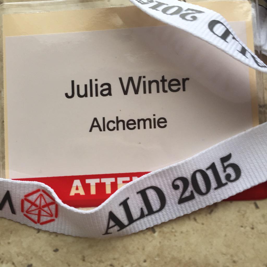
Julia Winter from http://www.alchem.ie gets her badge. Here you can also see that ASM has sponsored the key chain.

Seminars


Sunday Tutorials : Prof. Markku Leskelä, University of Helsinki, Finland, “ALD Process Development: Solutions to Industrial Challenges” Introduced by Prof. Winter. (Photo by Iain Buchanan)


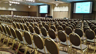
Chuck Winter opens AVS ALD 2015. Over 750 attendees (!) and 400+ abstracts (Sean Barry, Twitter)


Here is a picture showing quite clear how broad ALD has become these days (Picture from Martin Knaut).

 
Another shot when the before the first pulse of ALD Experts has been injected (Sean Barry, Twitter)


ALD manufacturing session: packed room (Angel Yanguas-Gil, Twitter


Mato Knez giving a plenary on ALD Beyond Electronics (Sean Barry)


The Golden Boy getting ready for his and Canadas great Golden Day - Session B, 9:15: the first ever robust ALD Au metal process. (Sean Barry, Twitter))


Very good talk by Conley on MIIM diodes (Angel Yanguas-Gil, Twitter)


Poster sessions


Our poster on the evolution of ALD is now up! (Angel Yanguas-Gil, Twitter )


Vincent Vandalon wins the graduate student award for best presentation at #AVSALD2015! We are so proud! http://t.co/LU69IPAr4Q


ALD Trade show


The leading supplier of high quality Atomic Layer Deposition (ALD) technology for industrial manufacturing (Picture by Timo Malinen)


Pall Corporation showing their latest filter technology : Learn about precursor #filtration for contamination control in adv. #ALD processes (Twitter)


Pall Corporation Booth at the ALD trade show (Picture from Rob Nine)

EpiValence Booth http://www.epivalence.com (Picture form LinkedIn, Simon Rushworth)


Dinners and Receptions


Applied Materials, Picosun, Air Products and NSI sponsored party (Sean Barry, Twitter).


Applied Materials, Picosun, Air Products and NSI sponsored party (Martin Knaut, http://www.katharinaknaut.com)


Iain Buchanan from Air Products selling tones of high-k precursor (Martin Knaut, http://www.katharinaknaut.com)


Barking at the Moon (Martin Knaut, http://www.katharinaknaut.com)

Portland Sightseeing


Saturday by Sean Barry (from twitter)


The Golden Team from Ottawa Canada has arrived in Portland : These #BarryLab adventurers drove in a (crappy) van from @ottawacity to #AVSALD2015 in Portland. Check out the bumper


Air Products flying in to Portland passing Mount Hood (Iain Buchanan)


Mount Hood (Martin Knaut, http://www.katharinaknaut.com)


View from the hotel (Tero Pilvi)


Same as above later in the evening at one of the Parties. (Julia Winter, Twitter)


Portland view - Moon and Mountain (Tero Pilvi, Instagram)


The Moon rolling in heading for Mount Hood (Martin Knaut, http://www.katharinaknaut.com)


Old Town Chinatown is the official Chinatown of the Northwest section of Portland. The White Stag sign, a former advertising sign, greets those traveling into Old Town on the Burnside Bridge (Photo by Marcel Junige).


Portland sunset (Photo by Marcel Junige).


Portland airport with Mount Hood in the background (Photo by Marcel Junige).


ASM International Hosts ALD Technology Seminar in Portland at AVS ALD 2015

ASM International N.V. (NASDAQ: ASMI and Euronext Amsterdam: ASM) today announces that it will be hosting a technical seminar in Portland, OR, US, on Tuesday June 30, 2015, the second day of the ALD Conference.


In this 'All about ALD' technology seminar, ASM and a distinguished guest speaker will address challenges and opportunities for ALD processes and equipment to manufacture next generations of micro-electronic devices.

The agenda is as follows:

5.30 pm Reception, drinks and food 
6.15-6.30 pm Dr. ir. Ivo Raaijmakers (ASM) - Welcome and introduction
6.30-7.00 pm Dr. Jeffrey Elam (Argonne National Laboratory) - "Selective ALD in polymers: sequential
infiltration synthesis for lithography and nanofabrication " 
7.00-7.20 pm Dr. Suvi Haukka (ASM) - " Present and future challenges of atomic layer deposition"

Following the presentations, there is room for open discussion and networking until 9.00 pm.

The ASM technology seminar will take place in the Skyline room I-II at the Portland Hilton, 921 SW Sixth Ave., Portland, OR, 97204 US. The room will open at 5:30 pm for invited attendees. Interested parties should contact Rosanne de Vries, +31 88 100 8569, rosanne.de.vries@asm.com.