Join the Critical Materials Council (CMC) Conference 2018, April 26-27 in Phoenix, Arizona. Get actionable information on materials and supply-chains for current and future semiconductor manufacturing.
Friday, July 21, 2017
Monday, July 17, 2017
Introducing the FlexAL-2D the ALD Plasma Processing System for 2D Materials
Oxford
Instruments’ ALD and 2D technical specialists have teamed up with
Eindhoven University of Technology research teams to develop the
innovative FlexAL-2D for atomic layer deposition (ALD) of 2D transition
metal dichalcogenides for nanodevice applications.
Source: AZoNano LINK
More information can also be found at http://www.oxinst.com/FlexAL2D
Source: AZoNano LINK
More information can also be found at http://www.oxinst.com/FlexAL2D
Saturday, July 15, 2017
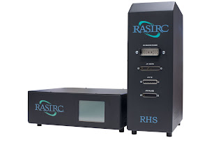
RASIRC Releases Next Generation RainMaker Humidification System for Fine Water Vapor Delivery
RHS Solves ALD delivery problems by eliminating particles and microdroplets at very high or very low flow rates
San Diego, Calif – July 15, 2017–RASIRC today announced the release of the next generation RainMaker® Humidification System (RHS). The system incorporates a new control system that provides highly accurate, droplet free water vapor for advanced atomic layer deposition (ALD) processes. The RHS has a wide mass delivery range of 50 - 5100 mg/min water mass flow rate in carrier gases. The system is capable of highly accurate and precise delivery of gaseous water into pressures from atmosphere to high vacuum.
“As demands for film quality and uniformity in ALD/ALE processes become increasingly challenging, process engineers have reached the limits with bubbler delivery methods,” said Jeffrey Spiegelman, President and Founder of RASIRC. “The RHS solves problems associated with process control and microdroplet formation, leading to better film uniformity and fewer defects.”
The next generation RainMaker® Humidification System (RHS)
Thursday, July 13, 2017
On the road to Denver for ALD2017?
Twitter is heating up with announcements of people and companies going to the ALD2017 conference in Denver 15 to 18 of July. Here is a selection of some of them. Please take a chance to download the conference app (see tweet below)
It is on, #ALDALE2017 pic.twitter.com/WnTjQFE4Hu— Scientist Tiger (@sean_t_barry) July 14, 2017
#ALDALE2017 the mobile app user name= ALD the password= Denver— AVS (@AVS_Members) July 12, 2017
Preperations for #ALDALE2017 :) pic.twitter.com/P6ibXx8yYY— Max Gebhard (@max_gebhard) July 13, 2017
Katja can't wait to present her study on #ALDep of copper at #ALDALE2017 @iivosen_tomi is eager too! pic.twitter.com/SA8KzjRq6B— HelsinkiALD (@HelsinkiALD) July 14, 2017
Just a few days to go @AvsAld conference (15-18 July). Visit us at booth #33 and speak to our #ALDep experts #ALDALE2017 pic.twitter.com/OeGsQ2h7rH— Oxford Instruments (@OxInst) July 13, 2017
Counting down to ALD2017! Come learn about our CVD/ALD #precursors & more at booth 34! #ALDALE2017 #CVDep #ALDep https://t.co/NBygrem21B pic.twitter.com/JxgkoTEbTu— Strem Chemicals Inc. (@StremChemicals) July 12, 2017
The George group will have a strong presence at #ALDALE2017 with 11 presentations. Find out more: https://t.co/JwKJ6YcAxV #ALDep #ALEtch— George Laboratory (@GeorgeGroupCU) July 11, 2017
Beneq is a proud platinum sponsor of #ALDALE2017. Visit our event website to get all the details. https://t.co/GrwxFnlz4b #beneqblog #ALDep pic.twitter.com/uGshtkGXof— Beneq Corporation (@beneqcorp) July 12, 2017
— kyle kimmerle (@pdxguy2009) July 15, 2017
Epivalence is Open for business #ALDALE2017 pic.twitter.com/A380ZOdII4— Simon Rushworth (@SARushworth) July 15, 2017
We're proud to be a platinum sponsor of #ALDALE2017, which is all about #AtomicScale processing. More info: https://t.co/jmmSC1c7Ud pic.twitter.com/izMQFfPIdo— LamResearch (@LamResearch) July 14, 2017
Film Sense and Kurt J. Lesker: in-situ Ellipsometry with the FS-1
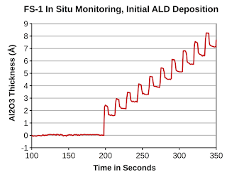
The Film Sense vision “to create easy-to-use and affordable ellipsometers” is especially relevant for in-situ applications. The Film Sense FS-1 realizes this vision by providing the power of Multi-Wavelength Ellipsometry, at an affordable price and compact size that is ideal for in-situ measurements. The FS-1 can provide real time thickness data with exceptional precision, which can be indispensable for the efficient development of new ALD processes. In the plot below, the “steps” in the data are direct observations of the thickness changes on the sample throughout the ALD cycles: the thickness increases and saturates as the precursor is introduced (trimethyl aluminum in this case), and then decreases as the film is oxidized (thermally by H2O in this case).
The relationship between Film Sense and
Kurt J. Lesker dates back to almost the inception of Film Sense. In fact, the first Film Sense FS-1 in-situ testing
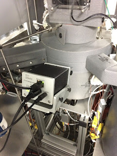
was performed on a Kurt J. Lesker ALD150LX reactor in 2014. The FS-1 has since been integrated on multiple
Lesker ALD reactors, and has been used to characterize a wide variety of thin
films including: Al2O3, TiO2, HfO2, and
TiN.
The
ALD150LX was designed from the ground up for advanced R&D and features
remote plasma as well as in-situ ellipsometry
as a primary means of real time process monitoring and control during ALD. Patented Precursor Focusing TechnologyTM
(PFTTM) prevents unwanted film deposition on sensitive surfaces
inside the reactor including the analytical port windows used for light transmission
during in-situ ellipsometry. The layout
of the plasma-enhanced ALD (PEALD) reactor makes installation and operation of
the compact FS-1 unit simple and easy.
According
to Bruce Rayner, Principal Scientist – ALD at the Kurt J. Lesker Company, “The
FS-1 provides excellent performance at a very attractive price, and its robust,
compact design is ideally suited for in-situ
ALD applications.”
If you are coming to ALD2017 in Denver,
please visit the Lesker booth #31 to see a live demonstration of the FS-1
integrated on an ALD150LX reactor. At
the Film Sense booth #1, an FS-XY150 automated mapping stage will be on
display.
The Film Sense FS-1 ellipsometer is now available
as an option for the Lesker ALD150LX reactor.
For more information please contact Dan Hadwiger (mailto:dhadwiger@film-sense.com) or
Noel O’Toole (mailto: noelo@lesker.com), or visit our websites at http://www.film-sense.com/products/fs-1-ald-applications/fs-1-lesker-ald150lx
and https://www.lesker.com/newweb/vacuum_systems/deposition_systems_ald_ald150lx.cfm.
RASIRC Presents TiN ALD Grown with BRUTE® Hydrazine at ALD Conference 2017
BRUTE Peroxide and BRUTE Hydrazine showcased in technical presentations
San Diego, Calif – July 13, 2017–RASIRC will announce the latest generation of its BRUTE Hydrazine product line at the annual ALD Conference held July 15-18, 2017 in Denver, Colorado. At low temperatures, ammonia or nitrogen plasmas cannot grow nitride ALD films on three dimensional, high aspect ratio (HAR) structures. BRUTE Hydrazine solves this problem and enables process engineers to incorporate nitrides into new device architectures.
RASIRC Chief Technology Officer Dan Alvarez will present “Low Resistivity Titanium Nitride ALD: Low Temperature Enabled by the Use of Ultra‐High Purity Hydrazine” on Tuesday July 18, at 1:45PM in Room Plaza F. Alvarez is a contributing author on another paper and two posters to be presented during the conference. RASIRC will also present the latest findings related to novel reactive chemistries for in-situ surface functionalization at Booth #16.
“The next generation of semiconductors require a new generation of precursors suited for low temperature, three dimensional deposition processes,” said Jeffrey Spiegelman, RASIRC President and Founder. “Our BRUTE chemistries meet these requirements, enabling surface functionalization, selective deposition, oxidation or nitridation without causing surface damage.”
“The next generation of semiconductors require a new generation of precursors suited for low temperature, three dimensional deposition processes,” said Jeffrey Spiegelman, RASIRC President and Founder. “Our BRUTE chemistries meet these requirements, enabling surface functionalization, selective deposition, oxidation or nitridation without causing surface damage.”
Tuesday, July 11, 2017
IC Deposition Materials Market Forecast of $1.2B by 2021
Precursors for metals and dielectrics in strong demand for finFETs and 3D-NAND
San Diego, CA, July 11, 2017: TECHCET CA—the advisory service firm providing electronic materials information—today announced that specialty chemical precursor market for the deposition of dielectrics and metals in integrated circuit (IC) fabrication is forecasted to increase at ~10% CAGR through the year 2021. TECHCET’s proprietary Wafer Forecast Model (WFM) shows that 3D-NAND devices are expected to grow at a rapid pace from 2016 and become one of the top three market segments by 2020. Logic ICs will continue to evolve, from 3D finFET devices to Gate-All-Around Nano-Wires (GAA-NW), enabled by new critical materials and manufacturing processes as detailed in new reports from TECHCET, “Advanced Insulating Dielectric Precursors,” and "ALD/CVD High-k & Metal Precursors."
Precursors tracked by TECHCET for ALD/CVD of metal and high-k dielectric films on IC wafers include sources of aluminum, cobalt, hafnium, tantalum, titanium, tungsten, and zirconium. The total market for 2017 is now estimated to be US$435M, growing to US$638M in 2021. The top-2 suppliers are estimated to hold more than half of the total available market, with many players competing to supply the next enabling molecule. In particular, cobalt precursor demand is forecasted to reach >$80M in 2021 as foundries transition to below 14nm-node processing. As a potential conflict mineral, TECHCET tracks the sub-suppliers of cobalt.
“Metal precursors have had double-digit growth over an extended period of time, and we expect that to continue as the IC industry transitions to 10nm- and 7nm-node logic and 3D-NAND fabrication, with an average long term CAGR of 11% over 2013 to 2021,” says Dr. Jonas Sundqvist, lead author of the report, senior technology analyst with TECHCET and researcher with Fraunhofer IKTS. “Dielectric precursors growth today is clearly driven by dielectric PEALD deposition in multiple patterning, and by dielectric CVD in 3D-NAND.”
Precursors tracked by TECHCET for ALD/CVD/SOD of advanced dielectric films on IC wafers include multiple sources of silicon. The total market for 2017 is now estimated to be just over US$400M, growing to US$560M in 2021. Current growth over 10% is expected to slow slightly to be in the 8-10% range over 2019-2021. Anticipated near-term developments include transitions from CVD to ALD for several IC fab modules.
Sunday, July 9, 2017
Argonne National Laboratory’s Continuous ALD Technology Licensed Exclusively to Forge Nano
LOUISVILLE, Colorado July 7, 2017: Argonne National Laboratory has entered into an exclusive license
agreement with Forge Nano to commercialize Argonne’s patented system and
method for continuous atomic layer deposition. This license enhances
Forge Nano’s ability to offer and protect key intellectual property
rights for its customers across an even broader array of strategic
markets.
Forge Nano’s innovative manufacturing systems are
industrializing the Atomic Layer Deposition (ALD) process by offering a
unique value proposition toward upgrading material performance for
wide-ranging applications. ALD is a process that deposits a uniform and
ultrathin encapsulating coating around any material. The process can
used to upgrade many materials, such as powders utilized in energy
storage applications (lithium-ion batteries, fuel cells,
ultracapacitors, etc.), as well as many non-energy applications as well.
ALD allows for coating thicknesses down to Angstroms (1/100,000th the
thickness of a human hair). Such control allows for the application of
coatings that are thick enough to eliminate unwanted reactions that
cause degradation within energy storage systems or moisture-sensitive
materials, yet thin enough to not adversely affect desirable material
properties. ALD coatings are by far the most compelling coating solution
for eliminating capacity fade and enabling higher overall performance
and safety in batteries. ALD is a process that has existed for decades
with hundreds of publications demonstrating its capability as a process
to improve material properties for a wide variety of applications.
However, due to a lack of manufacturing innovation, it has remained a
lab-scale process utilized primarily by academics. Forge Nano has
developed, patented and successfully demonstrated a high-throughput
process for applying ALD, which reduces the overall cost of energy
storage devices while improving their performance and safety.
Saturday, July 8, 2017
Fraunhofer IST use ALD to precision coat silicon spheres for the new kilogram standard
Precision work: defect-free coatings for silicon spheres
Fraunhofer IST Press Release / 4.7.2017More information on the ALD process and hardware can be found in this exellent presentation by Sanjeev Kumar Gurram, currently working as a consultant for Fraunhofer IST (LINK)
The prototype kilogram – to which all scales are calibrated to – is losing weight. International efforts are striving to redefine the base unit for measuring mass and, in future, redefine the kilogram on natural constants. For this purpose, the Avogadro experiment determines the number of atoms in almost perfect silicon spheres. Fraunhofer researchers have recently succeeded in homogeneously coating the spherical surfaces – the measurement uncertainty can be limited to a range below 10 micrograms.
The silicon sphere to be coated must be handled like a raw egg. On the right in the picture: one of the three-point mounts. © Photo Fraunhofer IST, Falko Oldenburg
Due to the fact that the prototype kilogram – the unit of mass upon which the weight of a kilo is based – is becoming increasingly lighter. The reason for this, however, is unknown. Now researchers are seeking alternatives for the platinum-iridium alloy artefact that is stored in a safe in Paris. The basic plan is to redefine the kilogram. In future, a physical constant will replace the material kilogram.
Thus, a team of scientists from the Physikalisch-Technische Bundesanstalt (PTB) (the national metrology institute of Germany) is conducting experiments with spheres of isotope-enriched silicon, which could be used as a new calibration standard. The experts, therefore, must determine the Avogadro constant, which indicates the number of atoms in one mole. ”We calculate the number of atoms in a sphere and use mathematical methods to obtain the number of atoms per mole. In simple terms, we find out how much a silicon atom weighs and through inverse conclusion can thus determine how many silicon atoms are needed for a kilogram,” explains Dr. Ingo Busch, physicist at the PTB in Braunschweig. ”The mole is the mediator between the atomic mass scale and the kilogram.”
Inside the ALD coating plant (a BENEQ TSF200) at the Fraunhofer IST: the coating chamber for three-dimensional objects. © Photo Fraunhofer IST, Jan Benz
Subscribe to:
Posts (Atom)


%20(1).png)


