Showing posts with label OLED. Show all posts

Thursday, July 28, 2016

Encapsulix SAS Introduces InfinityTM 200 Atomic Layer Deposition System

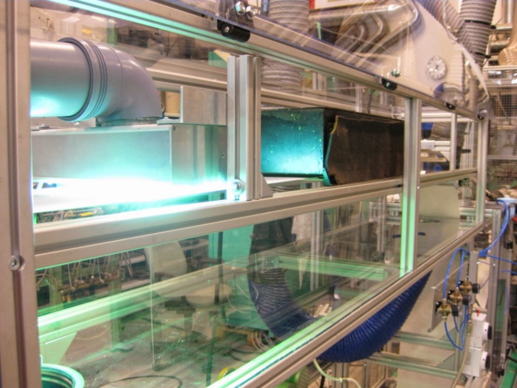
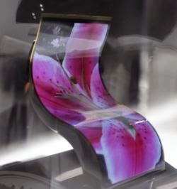
SIMIANE-COLLONGUE, France – July 26, 2016 – Encapsulix SAS today introduced its InfinityTM 200 Atomic Layer Deposition (ALD) system product line optimized for deposition onto 200 mm substrates in a manufacturing or R&D environment. The line’s advanced features for nano-engineered materials include a special focus on low temperature, thin-film encapsulation for flexible organic electronics, in particular organic light-emitting diodes (OLED).

The new 200 ALD line incorporates Encapsulix’s proprietary Parallel Precursor Wave (PPW) technology, which deposits atomic-level coatings with unmatched precision and throughput. The system has been successfully installed and qualified for ultrafast OLED encapsulation at Leti, the CEA Tech research institute in Grenoble, France. Additional systems will be delivered in the next 12 months to customers in Asia.

“We are pleased to strengthen our product offering to the OLED industry with this product family. The strategic partnership with Leti, and the successful application of our technology in the most demanding OLED encapsulation applications, confirm our position as the industry leader in ALD for OLED encapsulation,” said Dr. Jacques Kools, founder and CEO of Encapsulix SAS. “Our high-speed ALD thin-film encapsulation technology proves to be a key enabler in the flexible electronics revolution”.


Introduction to Encapsulix introduction, Dr. Jacques Kools, founder and CEO of Encapsulix SAS (Youtube).

“Since its launch in 2011, Encapsulix has continuously improved the performance of high-throughput atomic layer deposition equipment and processes,” said Dr. Tony Maindron, OLED senior scientist and project leader at Leti. “This new, ultrafast InfinityTM 200 system will strengthen Leti’s OLED development projects for next- generation wearable devices and other uses.”

The Infinity ALD equipment platform was developed by Encapsulix to address the microelectronic industry’s need for geometrically scaled nano-engineered coatings. These coatings range from 10-100 nm in thickness, and often are comprised of sublayers with nanometer thickness. The Infinity series provides the unique ability to transfer the process from R&D on 200 mm (resp. generation 2.5) in Infinity 200 (resp. Infinity 500) systems to manufacturing on generation 4.5 and generation 6 substrate sizes in Infinity 750 and Infinity 1000 tools. These capabilities provide a reliable route for quickly ramping the most advanced thin-film encapsulation solutions for flexible AMOLED.

About Encapsulix
Encapsulix was founded to address the geometric scaling of critical deposition requirements for industrial & microelectronic devices and foils. Initial process focus is in Al2O3 and TiO2 specifically for barrier coatings. The company has its development and headquarters in Simiane-Collongue France, equipment development, sales and service in the USA.

For more information:
Contact: www.encapsulix.com
Europe : Jacques Kools jkools@encapsulix.com

Wednesday, April 13, 2016

Beneq Introduces New Rotary Spatial ALD Solution

Today Beneq is reporting (Press release) : Beneq, a leading supplier of ALD equipment and thin film coating services, and Lotus Applied Technology, a technology development and licensing company working to break down the cost and throughput limitations of conventional Atomic Layer Deposition, today announced that they have signed a licensing agreement about Lotus Applied Technology’s Vortex ALD technology. Beneq will be using the technology developed by LotusAT in new rotary spatial ALD equipment that provides low process cost and high productivity in industrial ALD applications, such as barrier, passivation, insulation and protection applications for MEMS, LED, OLED, photovoltaics, memory, battery and sensors. 
 

A fast industrial solution for high performance coating of wafers

The new equipment will provide an optimal solution for ALD on wafers in industrial applications and will complement Beneq’s extensive portfolio of large-throughput spatial ALD solutions for industrial use, which already includes roll-to roll ALD equipment and continuous large-area ALD solutions for moving sheet substrates.

Monday, August 24, 2015

ALD Encapsulation technologies for flexible electronics

Here is an overview on encapsulation technologies for flexible electronics covering the main technologies and players. So just scroll down to the interesting part about ALD sating the main OEMs:
  • BENEQ
  • Lotus
  • Encapsulix
  • Synos (Veeco)
From a market perspective tehr is a forecast from IDTechEx Barrier Layers for Flexible Electronics 2015-2025: Technologies, Markets, ForecastsRead more at: http://www.idtechex.com/research/reports/barrier-layers-for-flexible-electronics-2015-2025-technologies-markets-forecasts-000409.asp


Barrier layer market forecasts in US$ million


Status of flexible encapsulation to enable flexible electronics


In 2020, flexible barrier manufacturing for flexible electronic devices such as displays will be a market worth more than US$184 million, according to IDTechEx Research. That equates to 3.8 million square meters of flexible barrier films for electronics.


Although multilayer approaches – usually organic and inorganic layers – have been the most popular solution for flexible encapsulation so far, there is significant development work with solutions based on single layer approaches such as flexible glass or atomic layer deposition (ALD) which could, in later years, capture part of the market. The table below, compiled by IDTechEx analysts shows some of the characteristics of flexible glass and ALD films as developers are looking to bring them to market.

[...]

Atomic layer deposition (ALD) present and future outlook/market share 

ALD is another flexible encapsulation technology receiving a lot of attention with several players currently developing solutions based on it. It seems like it is not a short-term solution, if it will ever be one as a stand-alone layer but ALD may be a solution in a multi-layer stack in combination with a sputtered or PECVD layer if it would be possible to find a good cost structure. Regarding the intrinsic properties of the material, ALD film deposited at low temperature (T<80 C) have a superior quality when tested at room temperature. A single ALD layer less-than 50 nm thick can perform better than thicker layers deposited by sputtering or PECVD.

However, the inherent stability of the films at higher temperature/humidity (e.g. 85C/85%RH) is a problem. If PE-CVD is used, ALD film stability improves, as well as for mixed oxides, but it is still an issue. A second problem comes with particles and substrates non-uniformity. Any defect may lead at an initial non-uniform nucleation that propagates into the growing film. Furthermore, loose particles on substrates may be partially covered, but because of the extreme thinness, the thin film does not have the mechanical strength to keep them in place under mechanical stress. Any mechanical stress leads to film fracture with consequent creation of an ingress path for moisture. That is why multilayer structures are necessary.

Deposition tools are in development from Lotus, Beneq, Encapsulix and others. Exploration at Samsung SDC with ALD films for TFE was very much advertised by Synos, but resulted in failure and any further evaluation was halted. ALD for barrier on foil has better results although there are doubts and hurdles in scaling up and reaching the deposition speed required for a cost effective process.


Friday, July 24, 2015

Video of a Visionox rollable OLED display in production 2017

OLED-Info just uploaded this amazing video of a truly rollable OLED display soon to go into mass production 2017 at Visionox in Mainland China - I do wonder if they use an ALD barrier to reach 3 mm curvature.


Wednesday, July 1, 2015

Kurt J. Lesker introduces new R&D Platform for organic material deposition, ALD and PEALD

Kurt J.Lesker's most affordable organic material deposition system platform, designed specifically with the entry to mid-level user in mind. Standard configurations compatible with up to 100mm x 100mm square or 150mm diameter substrates, up to 350°C heating and cooling, glove box option available.


  • Designed to accommodate specific organic and inorganic thin film applications such as, OLED Displays, Lighting, Organic Photovoltaics and Electronics.
  • Offers both organic and metal deposition capabilities in a single chamber.
  • Recipe driven computer system control with data logging option available.
  • Field tested and proven design.

Glovebox Interfaced System: Incorporates a sliding front door with glove box interface flange and sliding rear door for unobstructed chamber access. Facilitates thermal and plasma enhanced atomic layer deposition techniques

Standard chambers are configured to allow up to:

(12) 1cc, 10cc, or 35cc plug-in low-temperature organic sources

(4) Thermal evaporation sources and pellet feeder option

- Personalised combinations available based on system platform

- Scroll type rough pumping; cryogenic high vacuum pumping

- Standard configurations compatible with up to 8" x 8" (200mm x 200mm) square substrates, up to 350°C heating, glove box, up to five mask storage shelves with motorised transfer, and wedge tool options

- Basic computer control with recipe and data logging options are available as well

Wednesday, June 3, 2015

Fujifilm and imec demonstrate full-color OLED with photoresist technology for organic semiconductors

FUJIFILM Corporation (President: Shigehiro Nakajima) (hereafter, “Fujifilm”) and nano-electronics research institute, imec (CEO: Luc Van den hove), have demonstrated full-color organic light-emitting diodes (OLED)*1 by using their jointly-developed photoresist technology*2 for organic semiconductors, a technology that enables submicron*3 patterning. This breakthrough result paves the way to producing high-resolution and large organic Electroluminescent (EL) displays and establishing cost-competitive manufacturing methods.


Organic EL displays are increasingly used for televisions, mobile devices including smartphones as well as wearable devices. Since they can be made thin and flexible, while also offering excellent response time and contrast ratio. It is said that today’s products require organic EL displays of high pixel density, i.e. around 200ppi*4 for 4K televisions, 500ppi for full HD mobile devices and even higher density for compact displays for wearable devices. There has been active R&D for organic semiconductors to develop a high-resolution patterning method for organic EL materials to be used in these products. 


In 2013, Fujifilm and imec jointly developed photoresist technology for organic semiconductors that enables submicron patterning without damaging the organic semiconductor materials, based on photolithography*5 capable of high-resolution patterning on large substrates. There is no need for additional capital investment since an existing i-line exposure system can be used for the new technology. This is why the technology has attracted wide attention since the development announcement with anticipation of a cost-effective way of manufacturing high-resolution organic semiconductor devices.

In the latest achievement, Fujifilm and imec produced full-color OLEDs with the photoresist technology for organic semiconductors and successfully verified their performance. Red, green and blue organic EL materials were patterned, each in the subpixel pitch of 20μm*6, to create full-color OLEDs. An OLED array of 40 x 40 dots at the resolution of 640ppi was realized and illuminated with UV rays to confirm that red, green and blue dots separately emitted light. The emission of red, green and blue lights was also confirmed in a test involving the application of voltage rather than illumination, confirming its correct performance.

These results open new opportunities, such as using the novel photolithography in a multiple patterning process. An example would be creating an OLED array that adds a fourth color to red, green and blue, as well as developing previously-unseen devices such as a new sensors that integrate OLED with the organic photodetector*7.

This research result is to be presented at the SID Display Week, one of the world’s largest international exhibitions for information displays, held in San Jose, California from May 31 to June 5, 2015.

Since the commencement of joint research in November 2012, Fujifilm and imec have broken through the boundary of conventional technology to contribute to the progress of technology associated with organic semiconductors, e.g., developing the photoresist technology for organic semiconductors that enables the realization of high-resolution submicron patterns. The two companies will continue to undertake cutting-edge R&D involving semiconductor materials, process technology and system integration, thereby contributing to resolving challenges faced by the organic electronics industry.

Friday, May 1, 2015

OLED Encapsulation: technological introduction and market status | OLED-Info

OELD-info has a very good  technological introduction and market review on OLED encapsulation, whis you can read here. Check it out and read about the main players of ALD OEMs in this field as published by OLED-info:

OLED-Info
  • Vacuum Polymer Technology: developed at Vitex and bought by Samsung in 2010, this is the technology currently used by Samsung. It is a multi-layer barrier that is relatively slow to deposit as it requires several stages (SDC recently managed to reduce them from 6 to 3) and so Samsung is looking to replace it with a more cost effective solution.
  • LG's Faceseal: LG's own encapsulation technology, this is a a multi-layered organic and in-organic film. LG Display currently uses Faceseal for both flexible OLED display and lighting panels.
  • Atomic Layer Deposition (ALD): ALD can be used to quickly and efficiently deposit barrier films on flexible substrates. Several companies are developing OLED encapsulation systems based on ALD. One example is Veeco with their FAST-ALD tech (which they acquired in 2013 for $185 million) which is being evaluation by Samsung. Other OLED ALD developers include Beneq and Encapsulix.
  • Ink Jet Printing: While ink-jet is usually associated with micro-scale patterning, it can also be used to accurately and efficiently deposit encapsulation layers. In November 2014 Kateeva launched an Ink Jet Printing based Encapsulation system, and already shipped a mass-scale system - presumably to Samsung Display. 
  • PECVD: Plasma Enhanced Chemical Vapor Deposition (PECVD) is another deposition technology that can be adapted for encapsulation barrier films. In 2015 Aixtron acquired PlasmaSi, a PECVD OLED encapsulation developer - and plans to incorporate those systems into its OLED deposition clusters.
  • UniversalBarrier: This technology, developed by Universal Display (UDC), can be used to deposit single-layer encapsulation films. According to the latest update from UDC, the technology is not yet ready for mass production, but it is already being evaluation by Samsung Display.
  • Flexible glass: Yes, it is possible to make flexible glass - which is a great barrier, but still not as durable as thin-film encapsulation materials. Corning for example is promoting its Willow Glass as a possible flexible glass encapsulation (and substrate) technology.

Thursday, November 13, 2014

ALD for Light Emitting LED and OLED by Picosun

From AZ Materials: Over the past few years, the wafer-based semiconductor industry has been using the atomic layer deposition (ALD) thin film coating technique to develop a wide range of electronic products and components. For an improved level of system miniaturization and integration, thin films have to be uniform, dense and conformal, as well as free from pinholes, cracks and other defects.

When the preferred film thickness begins to approach nanometer scale, traditional thin film deposition methods such as PVD and CVD do not meet this requirement. In contrast, ALD forms excellent quality films even on the most complex nanoscale geometries. This can be attributed to its surface controlled and self-saturating film growth mechanism.

LED manufacturing is a wafer-based technology – similar to integrated circuit (IC) device manufacturing techniques. ALD is an optimal method that can be incorporated into current LED manufacturing processes and it can provide a wide range of benefits to the industry, either by introducing new manufacturing steps or replacing existing ones to extend the product lifetime, improve the device efficiency, or to save manufacturing costs.


Picosun’s PICOPLATFORM™ 200 vacuum cluster system for wafers up to 200mm diameter.

Currently a number of LED manufacturers across the globe are using Picosun’s ALD technology in their production. For OLEDs, Picosun delivers excellent ALD solutions to protect the devices against moisture

Full story here 

Sunday, November 9, 2014

Polymer hybrid thin-film composites for food packaging and membrane filters

As reported by VTT: Juha Nikkola M.Sc.(Tech.), Senior Scientist at VTT Technical Research Centre of Finland, developed new hybrid materials in his doctoral research project for use in the manufacture and modification of thin-film composites. The project resulted in new materials suitable for instance for food packaging with enhanced diffusion barrier and for membrane filters with improved anti-fouling properties used in water purification. In the future, similar materials may find use in flexible OLED displays and in wall and ceiling panels.

The doctoral research project involved developing surface materials that decrease bacterial adhesion to the surface. Improved surface materials can help keep membrane filters or wall surfaces clean or improve the preservation of food.

Food spoilage can be delayed with a new type of cardboard package coated with a plastic incorporating the thin-film composite structure developed in the present project. Such diffusion barrier materials may also find use in flexible OLED displays in the electronics industry or in replacing thickly layered paint on wall and ceiling panels.

The doctoral research project involved studying and developing flexible thin-film composites using various coating techniques and studying the impact of the surface layer on the permeability and anti-fouling properties of the thin-film composite. The hybrid materials developed can be produced in roll-to-roll processing. The research focused on atmospheric plasma deposition, atomic layer deposition (ALD) and sol-gel deposition techniques.


Thin-film composites can be manufactured using a roll-to-roll process. The photo shows the VTT coating production line.

A hybrid material is simply a combination of two materials at the macro, micro or nano level. Hybrid material is typically a blend, multilayer or nanostructured material. For instance, multilayer structures manufactured using thin-film deposition techniques can be named as hybrid materials.

Thin-film composites usually consist of three layers with different functions. The support and core layers provide the mechanical properties such as strength and flexibility. The core layer may also have properties affecting the chemical durability, permeability or composition of the composite. The properties required of the skin layer may have to do with separation efficiency, diffusion barrier performance, roughness, surface energy or liquid or gas permeability.

Juha Nikkola will defend his doctoral dissertation at the Tampere University of Technology on 31 October 2014 at 12.00.

The thesis is available online at Polymer hybrid thin-film composites with tailored permeability and anti-fouling performance: http://www.vtt.fi/inf/pdf/science/2014/S66.pdf


Tuesday, September 30, 2014

University of Michigan showcases 10x increase in the lifetime of blue phosphorescent OLED

 As reported by University of Michigan "Live long and phosphor: Blue LED breakthrough for efficient electronics" In a step that could lead to longer battery life in smartphones and lower power consumption for large-screen televisions, researchers at the University of Michigan have extended the lifetime of blue organic light emitting diodes by a factor of 10.

Blue OLEDs are one of a trio of colors used in OLED displays such as smartphone screens and high-end TVs. The improvement means that the efficiencies of blue OLEDs in these devices could jump from about 5 percent to 20 percent or better in the near future.
 
 
The blue PHOLED consisted of a thin film of light-emitting material sandwiched between two conductive layers—one for electrons and one for holes, the positively charged spaces that represent the absence of an electron. Light is produced when electrons and holes meet on the light-emitting molecules. (Picture from University of Michigan FLICKR)


Tenfold increase in the lifetime of blue phosphorescent organic light-emitting diodes

Yifan Zhang, Jaesang Lee & Stephen R. Forrest    
Nature Communications 5, 5008, 25 September 2014, doi:10.1038/ncomms6008 
Abstract:
Organic light-emitting diodes are a major driving force of the current information display revolution due to their low power consumption and potentially long operational lifetime. Although electrophosphorescent organic emitters have significantly lower power consumption than fluorescent emitters, the short lifetime of electrophosphorescent blue devices has prevented their application in displays for more than a decade. Here, we demonstrate a novel blue electrophosphorescent device with a graded dopant concentration profile in a broadened emissive layer, leading to a lower exciton density compared with a conventional device. Thus, triplet-polaron annihilation that leads to long-term luminescent degradation is suppressed, resulting in a more than threefold lifetime improvement. When this strategy is applied to a two-unit stacked device, we demonstrate a lifetime of 616±10 h (time to 80% of the 1,000 cd m−2 initial luminance) with chromaticity coordinates of [0.15, 0.29], representing a tenfold lifetime improvement over a conventional blue electrophosphorescent device.

Tuesday, April 15, 2014

Beneq is joining forces with German MBRAUN for OLED

In a press release on April 15, 2014, Beneq announced that it is joining forces with MBRAUN to address the growing OLED market needs by offering turn-key R&D solutions. The goal is to enforce rapid adaptation of Beneq’s breakthrough thin-film encapsulation technology in OLED research and manufacturing.

Beneq and MBRAUN currently have a mutually supportive offering, which will allow customers to get a wider portfolio of products and services from a single source. These products are primarily targeted to those customers with sophisticated needs in OLED research, especially in the area of thin-film encapsulation. For each customer need, Beneq and MBRAUN will work together to tailor products and services that best meet the specific clean environment requirements in question.
 
 
Beneq and MBRAUN are joining forces to boost thin film encapsulation for OLED research and manufac-turing. Picture: Beneq.
 
More details can be found here in this slide share file.
 

Saturday, March 1, 2014

French ALD Equipment supplier Encapsulix has shipped a deposition system to a leading OLED lighting supplier in Europe

The french ALD Equipment supplier Encapsulix based in Aix-en-Provence has announced that a Gen-2.5 deposition system has been shipped to a "leading OLED lighting supplier in Europe".Encapsulix announced tin October 2013 hat they received such an order and this should then be the shippment - congratulations!
 
"Encapsulix announced today the sale of an Infinity(tm) 500 manufacturing equipment to a leading OLED lighting manufacturer for Atomic Layer Deposition Encapsulation.
 
The Infinitytm 500 has been developed utilizing Encapsulix’s patented & proprietary Atomic Layer Deposition technology. The Infinitytm 500 product family deposits barrier and encapsulation films on substrates up to 500mm x 400mm and is the work horse for Gen2 OLED applications. The order received from a leading OLED lighting manufacturer is scheduled to be delivered end of 2013. The system provides the best ultrabarrier performance and cost of ownership for the manufacturing of OLED devices. The Infinitytm 1000 for Gen5 and 5.5 will be introduced in 2014 along with the Infinity tm Flex500 and 1000 for flexible organic substrates and rolls."
 
According to the information on the webpage the inovation in Encapsulix ALD technology lays in an assembly of modular precursor dosers and gas injectors that behave as a monolithic “unit”
 
 
Picture from a patent : Gas injection device with uniform gas velocity US 20130019978 A1
  • Assemble application-specific systems based on common technology bricks
  • Factor of 5-100 throughput increase through massive parallel deployment
  • Commonality in hardware, Process between R&D, Prototype, Manufacturing

Wednesday, February 26, 2014

Encapsulation solutions from Dresden presented at ICCG 10

Encapsulation solutions from Dresden presented at ICCG 10
 
As reported in a press release: "The industrial product development focuses more and more on flexible electronics. Thus the technology of organic electroluminescence is on the verge of being launched onto the market. Therefore, high-quality functional films are required in reasonable quantities for the industrial manufacturing of flexible electronic devices. Flexible solar cells based on inorganic or organic semiconductors and flexible organic light-emitting diodes (OLED) provide new possibilities for the integration of photovoltaic or intelligent lighting in buildings and commodity items. Even flexible displays or innovative packaging concepts for pharmaceutical and cosmetic products are on their way to commercialization. All mentioned products have one thing in common: The active layers have to be protected from humidity and oxygen in order to guarantee a reliable functionality over the product lifetime.
 
Currently, the encapsulation technologies for these flexible electronic devices are mostly still in the research or pilot stage. The cluster FLEET – a Fraunhofer initiative - combines the competences of three Fraunhofer Institutions (FEP, IWS and COMEDD), one institute of the Technical University Dresden (IAPP) and one medium-sized company (SEMPA Systems) in this area of expertise. The intention of the cluster is the fast further development of encapsulation technologies to make them ready for the industrial and serial production, by an intensive cooperation along the value chain concentrated at one location."
 
Cluster FLEET will presents its expertise at ICCG 10 (The International Conference on Coatings on Glass and Plastics - Advanced Coatings for Large-Area or High-Volume Products) from 22nd until 26th June 2014, in Dresden.
 
 
You can save more than 25% with the early bird fee and register until March 3, 2014 for the event.
 
Furthermore there are a lot of sponsoring opportunities. Book your exhibition space here for presenting your services and products to  an excellent community of experts. Fraunhofer COMEDD will also offer a company tour on Friday, June 27, 2014. You can register for it also at the organizer of the conference.
 
For all information regarding sponsorship, preliminary program as well as the registration form, please take a look at the homepage: http://www.iccg10.de/


Saturday, February 22, 2014

Interview with Beneq's technical sales director ALD-based OLED encapsulation technology

Interview with Beneq's technical sales director ALD-based OLED encapsulation technology:

"- ALD is the only truly conformal and pinhole-free thin-film encapsulation technology. Due to the pinhole-free nature of ALD films, ultra-thin layers (i.e. 10’s of nm's) of inorganic material (e.g. Al2O3) is sufficient for OLED encapsulation. Ultra-thin layers are also compatible with future needs for flexibility. Conformality is advantageous e.g. in elimination of side-diffusion, the OLED device can extend to the very edge of the device and still be reliably encapsulated. Finally, the ALD material costs are very low, and overall cost-of-ownership is very competitive.


- ALD is uniquely well suited for flexible OLEDs, due to the ultra-thin layers which are compatible with the future flexibility requirements. I would go as far as to say that ALD will enable future flexible OLED products."

- Beneq's director of Technical sales, Mikko Söderlund
 
Complete Interview with some interesting insights into the ALD OLED business and also comments with respect to Synos/Veeco Fast-ALD(TM) technology.
 
 
For more information on all kind of OLED Technology this site has a lot to offer on flexible OLED and all othe topics as well: http://news.oled-display.net

 
The film stack building up an OLED on a flexible substrate such as flexibel glass, plastic or a metal foil (schematic above from OLED-Display.net).
 
According to Erich Strasser at OLED-Display.net there are the development and market entry stages:
  • very thin > 0.25mm, light, unbreakable
  • Bendable, ready for production (Galaxy Round, LG-Flex)
  • Rollable, completely flexible –> ready 2016
  • Printable, displays like a paper –> ready 2018-2020


Thursday, February 20, 2014

Veeco ship first Prototype System for FAST-ALD™ for OLED to Samsung

According to the 4Q/2013 results press release  Veeco book first Prototype System for FAST-ALD™
 
"while not included in reported fourth quarter bookings, we received a purchase order from the world leader in mobile OLED displays for a next generation Fast Array Scanning Atomic Layer Deposition (FAST-ALD™) prototype system."


Recent information has become availabel that the system is heading to Samsung "Veeco sold a FAST-ALD flexible OLED encapsulation prototype system to Samsung". Who else could it bee since Samsung has 95% of that market? It is also in lign with previous reports on Synos Technology working with Samsung for Flexible OLED encapsulation.


Check out the cool animated video below to understan more about FAST-ALD a.k.a. Spatial ALD. Further reading on this technology you can find on the Veeco page for FAST-ALD : http://www.veeco.com/promos/fast-ald.aspx, where the key benefits are listed as:
 
  • Ultra-fast ALD process with continuous substrate scan Large substrate scalability without losing process throughput
  • Excellent uniformity with closed loop linear reactor design
  • Low CoO with high efficient gas-solid reaction process
  • Simultaneous In-line multi-process capability
 

Other companies that are developing or producing Spatial ALD Equipmet: