Showing posts with label ALD. Show all posts

Tuesday, January 16, 2018

Picosun collaborates with ST in 300 mm power semiconductors

ESPOO, Finland, 16th January, 2018 – Picosun Oy, a leading supplier of Atomic Layer Deposition (ALD) thin film coating technology for global industries, partners with STMicroelectronics S.r.l. to develop the next generation 300 mm production solutions for advanced power electronics.

Power electronic components are right at the heart of many core elements of our society, where energy saving, sparing use of natural resources, and CO2 emission reductions are called for to provide for sustainable future. Energy production with renewables such as wind and solar, clean transportation with electric vehicles and trains, and industrial manufacturing with energy-smart power management and factory automation are key markets where the demand for advanced power components is increasing.


Most power semiconductor industries use 200 mm wafers as substrates. Transfer to 300 mm enables more efficient, ecological, and economical production through larger throughputs with relatively smaller material losses, and adaptation of novel manufacturing processes such as ALD allows smaller chip sizes with increased level of integration.

As a part of the funded project R3-POWERUP (*), Picosun’s PICOPLATFORM™ 300 ALD cluster tool will be optimized and validated for 300 mm production of power electronic components. The SEMI S2 certified PICOPLATFORM™ 300 cluster tool consists of two PICOSUN™ P-300S ALD reactors, one dedicated for high-k dielectric oxides and one for nitrides, connected together and operated under constant vacuum with a central vacuum robot substrate handling unit. The ALD reactors are equipped with Picosun’s proprietary Picoflow™ feature which enables conformal ALD depositions in high aspect ratios up to 1:2500 and even beyond. Substrate loading is realized with an EFEM with FOUP ports. The fully automated cluster tool can be integrated into the production line and connected to factory host via SECS/GEM interface.

“Our PICOPLATFORM™ 300 cluster tools have already proven their strength in conventional IC applications, so expansion to the power semiconductors is only natural. We are very pleased to work with a company such as STMicroelectronics to tailor and validate our 300 mm ALD production solutions to this rapidly growing market. This is also a prime opportunity both to contribute to the future of European semiconductor industries, and to utilize ALD to provide technological solutions to the global ecological and societal challenges such as climate change and dwindling natural resources,” summarizes Juhana Kostamo, Managing Director of Picosun.

Saturday, January 13, 2018

MPD Chemicals Acquires Specialty Chemical Manufacturer Norquay Technology

Norqay Technology, a company with more that 30 years experience in organo metallic precursors for ALD and CVD has just been acquired by MPD Chemicals. Please find press release below.

TREVOSE, Pa., Jan. 11, 2018 /PRNewswire/MPD Chemicals (MPD), a US-based manufacturer of specialty chemicals and custom synthesis solutions, announced today the expansion of its manufacturing capabilities, product portfolio and customer base with the acquisition of Norquay Technology, Inc. (Norquay). Located in Chester Pennsylvania, Norquay is the fourth acquisition to be integrated into the MPD Holdings platform, an Addison Capital portfolio company; existing MPD businesses include Monomer Polymer & Dajac Labs, Silar, and IsoSciences.

Norquay is a specialty chemical manufacturer with over 30 years of expertise in providing the scale-up and production of advanced proprietary custom materials, including organometallic, inorganic and organic molecules. Norquay’s product line includes chromic, electronic, catalyst, ligand, medical adhesive and UV performance products, with a customer base that ranges from startups to large multi-national corporations.

Saturday, November 25, 2017

The 7nm race by TSMC and Samsung - EUV or not EUV

According to industry sources on October 19, Samsung Electronics is considering a plan to purchase 10 extreme ultraviolet (EUV) lithography tools from the Netherlands-based ASML, the biggest semiconductor equipment maker in the world. To put tha in perspective - ASML believes that it can produce about 12 EUV lithography tools this year. It is the only company that manufactures EUV lithography tools in the world.

Sales in ALD and Etch equipment have been boosted by multiple patterning technologies based on Immersion lithography, both for Logic/Foundry and Memory. Maybe as much as 1/3 of the single/multi wafer ALD equipment market is patterning related. The last two years or so analyst have been busy trying to figure out the impact on deposition and etch equipment sales if/when EUV is introduced. Here is a recent take down by Seeking Alpha (LINK). My view is that scaling is based on symbiotic use of the latest technologies and multiple patterning and EUV will co-exist and keeping the scaling path alive. In addition, scaling opens new opportunities for ALD, ALEtch and future use of selective growth technologies with atomic scale precision. According to recent reports the ALEtch market segment is now considerd an actual segment by itself and has entered HVM (LINK).
Fudzilla reports: Korean based ETNews has mentioned that Qualcomm 7nm manufacturing has been a big win for TSMC while two other US and China customers chose Samsung’s 7nm. TSMC traditionially have dibs on Nvidia and MediaTek according to the report.

Qualcomm and Broadcom, according to the report are designing their next generation chips with TSMC’s7-nano PDK. The reason why Qualcomm went with 7nm with TSMC is the fact that the fab uses normal steppers while Samsung wants to make its 7nm with more bold and riskier EUV (Extreme Ultraviolet) photolithography technology.

View of Samsung Electronics’ Hwasung 17 line. It is expected that Samsung Electronics will build a new 7-nano plant on a nearby site according to ETNews.

Samsung is expected to be later to the 7nm game and early adopters had to go with TSMC. EUV is still technology that is not entirely ready for the mass market and there is a disagreement weather you should need to use Extreme Ultraviolet light manufacturing with 7nm or first with 5nm. Obviously the two main fabs disagree while GlobalFoundries cooperates and shares technology with Samsung, and will have Samsung to rely upon for 7nm.

Full article: Qualcomm 7nm made by TSMC [LINK]
ETNews original source: Samsung Electronics Close to Securing Two New Customers for Its 7-Nano Foundry[LINK]
Business Korea: Keeping Leadership in 7-nano Era Samsung Electronics Seeks to Buy Up Next-gen Semiconductor Mfg Equipment

Saturday, November 18, 2017

Aixtron complete sale of ALD/CVD memory product line to Eugene Technology

AIXTRON SE (FSE: AIXA), one of the world’s leading providers of deposition equipment to the semiconductor industry, announced today that the sale of AIXTRON’s ALD and CVD memory product line to Eugene Technology Inc., a wholly owned U.S. subsidiary of Eugene Technology Co., Ltd, South Korea was completed as of November 15, 2017. 

The QXP-8300 Atomic Layer Deposition (ALD) mini-batch system suitable for e.g. high-k oxide films in advanced memory applications including 3D structure devices (aixtron.com)

AIXTRON will receive c. USD 60 million for the assets being transferred and c. USD 11 million for open supplier orders for which it retains the liability to pay.

AIXTRON, Inc., the U.S. subsidiary of AIXTRON SE situated in Santa Clara, California, will continue to provide sales and support for its continuing businesses.

Friday, November 10, 2017

Picosun Oy shows record growth in ALD for fiscal year 2016/2017

Picosun is one of the leading suppliers of ALD thin film deposition technology for semiconductor, lightning, MEMS as well as for other industries and research. This week I had the chance to meet with Kustaa Poutiainen himself, Chairman and Chief Executive Officer of Picosun Oy. in Dresden. We had a very interesting meeting discussing recent developments in ALD Technology announced by Picosun as well as discussing the past and future outlook of ALD.   

Mr Poutiainen was in Germany to meet with customers and overseeing Picosuns activities and expansion in Germany. In the European perspective Germany is the biggest market for ALD Technology and Equipment. For those of you who do not know, Picosuns ALD equipment portfolio in detail it ranges from fully automated ALD batch and cluster systems for high volume manufacturing to smaller scale R&D and pre-pilot production tools (see below). 


A snapshot of the Picosun products - more information here.
Picosun has recently opened a branch office in Germany - Picosun Europe GmbH, headed by General Manager Dr. Christoph Hossbach, serving its growing install base of ALD equipment on the German market, both at leading research institutes within Fraunhofer and other research organizations and wafer fabs. According to previous press releases made we know that they have a number of high value customers in Germany including Bosch Sensortech.

Mr Poutiainen was very excited over the development of Picosun as a company and informed me that it ended its Fiscal year 2016/2017 in September by a record turnover growth of 27% landing at just above 21 million EUR for 2016/2017 and more details will be released soon. The company is constantly investing to develop it operations further globally adding new local teams and having a strong focus on R&D. Mr Poutiainen did also let me know that Picosuns R&D expenses are at about 20% of the actual turnover, which is considerable. Quoting Mr Poutiainen: “The most awarding proof of success of the company is to hire new members. We are looking to hire more than 30 new employees in the next expansion phase”.
Next you have a chance to meet Picosun at SEMICON Europa in Minich. Picosun is exhibiting as well as sponsoring the ALD Lab Saxony Symposium on the 14th of November.
ALD Lab Saxony Symposium : LINK


Wednesday, November 1, 2017

Save the date: 2nd HERALD.ECI Workshop in Barcelona

Following the HERALD.ECI network kick-off : June 14, 2017 in Linköping, Sweden, and the 1st HERALD.ECI Workshop on Career Development : August 28-29, 2017 in Ghent, Belgium 2nd HERALD.ECI Workshop with hands-on training for “bonding HERALD.ECIs from ideas to proposals”
organized by Mariona Coll, Maximilian Gebhard, and Marcel Junige

When? March 01-02, 2018 

Where?  ICMAB (Institut de Ciència de Materials de Barcelona) in Barcelona, Spain

Tentative program

The main objective of this 2nd HERALD.ECI Workshop with hands-on training is to create an ignition point for competitive proposals resulting in joint, EU-funded research projects under ECI (early career investigator) participation or leadership.
We want the trainees to
  • gain advanced ‘theoretical’ knowledge input on how to write competitive proposals & manage EU-funded projects from an EU funding expert & Horizon 2020 coach through an impulse talk plus interactive proposal clinics.
  • find excellent, perfectly matching collaboration/ project partners during a welcome mixer.
  • exchange experiences with an excellent (female) ALD expert and with an industry partner.
  • transfer the newly gained knowledge into advanced ‘practical’ skills by
    developing joint proposal ideas,
    transitioning specific ideas into concrete proposal drafts, and
    starting to write
    together in smaller, matched collaboration/ project groups.
  • go home with a raw outline and concrete idea description, i. e. the first step of an actual proposal.

Registration

More information will soon be available here: www.junige.de/herald-eci
Online registration will open early November 2017. The number of participants is limited to max. 25 HERALD.ECI network members.

Accommodation

We suggest accommodation for attendees at the VILA UNIVERSITARIA.
A contingent of 15 rooms is reserved until December 15, 2017.
To book your room there, please use the following .pdf form.
 

COST Travel Grants

COST Travel Grants are available upon request for 10 trainees from ITCs (inclusiveness target countries);
i. e. Bosnia-Herzegovina, Bulgaria, Cyprus, Czech Republic, Estonia, Croatia, Hungary, Lithuania, Latvia, Luxembourg, Malta, Montenegro, Poland, Portugal, Romania, Slovenia, Slovakia, the former Yugoslav Republic of Macedonia, Republic of Serbia and Turkey.

ECI (early career investigator)

Within HERALD, the ECI network aims to promote the next generation of young ALD scientists and help to establish themselves as research leaders in the ALD community.

This HERALD.ECI Workshop is supported by COST (European Cooperation in Science and Technology). COST is supported by the EU Framework Programme Horizon 2020.
COST Action MP1402 - HERALD
Hooking together European research in Atomic Layer Deposition

Monday, October 30, 2017

New high-throughput platform for studying TiO2 photocatalytic oxidation reactions

Researches from University of Helsinki  present a new high-throughput platform for studying titanium dioxide (TiO2) photocatalytic oxidation reactions.


Wednesday, October 25, 2017

Aixtron's sale of ALD/CVD Product Line to Eugene Technology in South Korea gets US approval

Aixtron SE (AIXG), announced Tuesday that the Committee on Foreign Investment in the United States or CFIUS has approved the sale of ALD and CVD memory product line. 
 
 
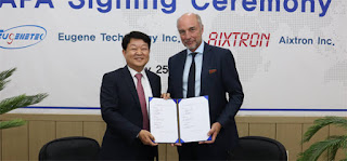
Eugene Technology CEO Eom Pyeong-yong (left) and Aixtron CEO Kim Schindelhauer pose for a photo holding their contract. (Picture credit: Pulse by Maeil Business Newspaper & mk.co.kr LINK)
 
The company noted that the investigation by the CFIUS of the sale of AIXTRON's ALD and CVD memory product line to Eugene Technology in South Korea resulted in a determination that there are no unresolved U.S. national security concerns from CFIUS' perspective.
 
Full report: LINK

Tuesday, October 24, 2017

Picosun’s ALD technology improves lifetime and reliability of electronic circuit boards

ESPOO, Finland, 24th October, 2017 – Picosun Oy, leading provider of advanced Atomic Layer Deposition (ALD) solutions for global industries, has invented an ALD-based method(*) with which the operational lifetime and reliability of printed circuit board assemblies (PCBA) can be efficiently improved.

Metal whisker formation and corrosion are some key factors that cause PCBA performance degradation over time. Metal whiskers are thin filaments or threads growing out from solders, components, and interconnects on the PCBA, and they can cause short-circuiting that leads to a system failure. This is particularly fatal in several sensitive applications such as medical, automotive, space, aviation, military, and industrial control electronics. 
Previously, lead has been added to solder alloys to prevent whisker formation, but the current environmental regulations prohibit its use. This is why novel methods, such as the ALD-based surface protection technique developed and now industrially enabled by Picosun are very much sought after amongst the electronics manufacturers. In Picosun’s approach, application-specifically tailored ALD nanolaminate forms a dense, conformal, and hermetic seal on the PCBA. This seal protects the PCBA components from the corrosion caused by moisture and impurities in the ambient air and blocks the metal whisker propagation. As ultra-thin films, ALD coatings have the additional benefit of allowing postprocessing of the PCBA, and they do not increase its mass or dimensions. Furthermore, as a gas-phased technique, ALD is gentle to the surface, it can be applied at moderate temperatures, and it is environmentally friendly.


“Our PCBA protection technology has gained lots of interest amongst our clients both in industries and in R&D, and many are eager to start applying it in their manufacturing processes. Electronic circuit board industry is a vast, global market, where we are happy to utilize our ALD knowhow to enable products of extended lifetime and improved safety and reliability. Our comprehensive selection of industrial ALD systems guarantees an optimal solution to every customer, allowing fast and economic processing of even large area PCBAs in just one process run,” states Juhana Kostamo, Managing Director of Picosun.
(*) Pat. pending

Thursday, October 19, 2017

Conductance measurements optimize atomic layer deposition automatically

As reported by nanotechweb.org: An in situ measurement technique that can monitor the process of atomic layer deposition (ALD) in real time has been developed by scientists in Germany. The researchers used changes in the conductance of layers over multiple ALD cycles to identify the different growth phases as they occurred, allowing undesired modes of deposition to be averted. The conductance signal was also used as the input to a genetic algorithm that could optimize the growth rate semi-automatically.