Oxford Instruments, a company that truly master both Atomic Layer Deposition and Atomic Layer Etching, will be giving two talks at the Joint ALD2016 Conference and ALE2016 Workshop in Dublin, Ireland in less than two weeks. Naturally one on each topic!
Oxford Instruments is Platinum sponsor of the conference and you will have an opportunity to meet with their Deposition and Etch Experts at the Exhibition and Social events.
Harm Knoops
Oxford Instruments Plasma Technology, UK / Researcher at TU Eindhoven, NL
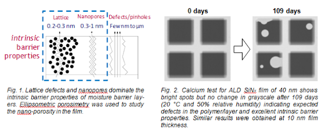
Low-temperature plasma ALD of silicon nitride moisture barrier layers
Wednesday 27 JULY: Silicon-based materials - Wednesday 27 July 14:00-15:30
15:15-15:30
ALD has demonstrated to be able to provide excellent moisture barrier layers, which are vital for the encapsulation of organic (opto-)electronic devices, such as organic light-emitting diodes (OLEDs) and thin-film photovoltaic cells. Very low water vapor transmission rates (WVTR) have been shown using oxide layers prepared by ALD (Al2O3 and TiO2) but not yet for nitride layers. In this work, moisture permeation barrier layers of SiNx prepared by ALD using SiH2(NHtBu)2 (BTBAS) precursor and Ar-N2 plasma were investigated.1 Intrinsic WVTR values in the range of 10−6 g/m2/day were obtained, indicating excellent barrier properties for ALD SiNx layers as thin as 10 nm.
Mike Cooke, CTO
Oxford Instruments, UK
Atomic layer etching (ALE) in close-to-conventional plasma etch tools
Tuesday 26 July: Plasma-enhanced deposition and etching - Tuesday 26 July 15:45-17:15
15:45-16:15
Plasma etching equipment and expertise is widespread, and cyclical etch processes are well known for high rate silicon etching. With the recent surge in interest in atomic layer etching, many groups are attempting to perform ALE in their existing tools. This talk discusses the limitations and options of using conventional tools for ALE, and gives results for both conventional and modified equipment.
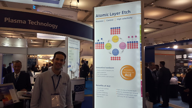
Oxford Instruments releasing new innovative hardware for ALE (Atomic Layer Etching) Harm Knoops at SEMICON Europa 2015, Dresden, Germany.
In addition, you may be interested in talk given by Dmitry Suyatin on III/V Nanowire splitting by ALE - work all performed on an Oxford Instruments Plasmalab 100 at Lund Nano Lab, Sweden
Dmitry Suyatin
Staff Engineer, Lund Nano Lab, Lund University, Sweden
Monday 25 July, Monday 25 July 13:45-15:15
Liffey Hall 1
Workshop: Non-traditional ALE approaches
Liffey Hall 1
Workshop: Non-traditional ALE approaches
To study the ALE process for III/V nanowires GaP nanowires were grown by metal organic vapor phase epitaxy (MOVPE) from gold seed particles on GaP substrates and then mechanically transferred to Si surface. An ALE process optimized for Si etching was used to etch the GaP nanowires by applying a 30 nm (105 cycles) etch recipe. Surprisingly, we discovered that we were able to split the nanowires longitudinal into too wires (as shown in Figure 1, below).


%20(1).png)


I certainly appreciate your stuff provided in the blogs.
ReplyDeleteCleaning Services Oxford