Thursday, March 10, 2022
Beneq fulfills customer demand for tailored ALD equipment services and support with BeneqCareTM
Tuesday, March 8, 2022
RASIRC Granted Patent for Controlled Delivery of Hydrogen Peroxide Gas
Novel method for generation of H2O2 gas granted patent in US and Japan
Saturday, March 5, 2022
The Emergence of Hydrazine (N2H4) in Semiconductor Applications
Historically, metal-nitride
MOCVD and ALD films have been fabricated with Ammonia (NH3). However, lower thermal budgets and shrinking 3-dimensional
structures are needed for next generation semiconductor devices. These challenges have exposed limitations
with ammonia which could be overcome by replacing ammonia with hydrazine (N2H4). Purity of commercially available hydrazine has delayed its adoption. RASIRC Inc. has recently developed a new
formulation of hydrazine called BRUTE® Hydrazine which is safer and meets
purity requirements for semiconductor manufacturing. Prior to Brute Hydrazine,
the body of technical data applicable to semiconductor processing was limited
and scattered. This paper provides an
overview of the growing activity in the thin film use of Brute hydrazine as
well as early references on laboratory grade hydrazine for historical
completeness.
Increasing
Need for More Reactive Nitrogen Sources
Emerging devices
such Logic and Advanced Memory require high quality thin (5-20 Å) electrode and
barrier films. Difficult thermal budget
constraints are now being placed on well-known materials such as SiNx,
TiNx and TaNx.1-3 Deposition temperature limitations have dropped
to 350°C and below while very low resistivity (<150 micro-ohm/cm) for TiN
and TaN must still be achieved. Although
metal and nitride films grown using plasma assisted processes (PE-ALD) and
(PE-CVD) at low temperatures exhibit enhanced properties, the damage induced by
plasma on sensitive substrates is one of the common drawbacks,4,5 as
well as inability to support HAR or three-dimensional structures like
horizontal vias and deep trenches.
In addition to growing thin nitride films, hydrazine can also act as a reducing agent for several late transition-metals. This work is highly relevant to the use of hydrazine as a surface cleaning agent as well as a potential adder for metal ALD.7
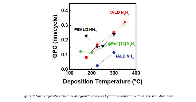
Figure 1: Low Temperature Thermal ALD growth rate
with Hydrazine comparable to PEALD with Ammonia.
The following table provides primary references for the areas of hydrazine ALD/CVD relevant to Semiconductor device applications. Additional relevant references on related films are also included.
|
Precursor and
Temperature |
Film |
Reference |
|
Al surface nitridation 200C-450C |
AlN |
Taylor
et.al. U.S. Patent 6465350, 2002 |
|
TMA MOCVD
300C-400C |
AlN |
Fujieda, S. et. al. Adv.
Func. Mat. 1996, 6(3), 127-134 |
|
TDEAA 150C-225C |
AlN |
Abdulagatov, A.I. et. al. Russian Microelectronics, 2018,
47(2), 118–130. |
|
TMA 175C-350C |
AlN |
Jung, Y.C. et. al. Materials 2020, 13, 3387; https://doi:10.3390/ma13153387 |
|
TDMAA 225C-400C |
AlN |
Ueda, S.T. et. al. Appl.
Surf. Sci. 2021, 554, 149656 |
|
BCl3 ,
350C |
BN |
Wolf, S. et. al. Appl. Surf. Sci. 2018, 439, 689–696 |
|
Surface Clean 200C |
Cu |
Hwang, S.M. et.
al. ECS Trans. 2019, 92, 265 |
|
Surface Clean 100C-300C |
Cu, Co |
Hwang, S.M. “Effect of
Surface Cleaning Efficacy on Vapor-Phase Cleaning of Cu and Co Using Anhydrous
N2H4” AVS ALD/ALE 2021 Session: Area Selective ALD AS4-1 |
|
TMG, 400C-800C |
GaN |
Fujieda, S. et.
al. Jpn. J. Appl. Phys. 1987,
26, 2067-2071 |
|
TMG, TMI, 600C-900C Theoretical |
GaN, InGaN |
Koukitu, A. et. al. phys. Stat. sol. (b), 1999,
216(1), 707-712 |
|
TMG Theoretical |
GaN |
Goddard, W. et.al. J. Phys. Chem. C 2015, 119(8) 4095–4103 |
|
[Ru(DMBD)(CO)3] 200C. Metal Deposition |
Ru |
Cwik, S. et. al. J. Vac. Soc. Sci. & Tech. A 2020, 38, 012402; https://doi.org/10.1116/1.5125109 |
|
SiH4 550C-1050C |
SiN |
Yoshioka, S. et. al. J.
Electrochem. Soc. 1967, 114, 962–964. |
|
SiH4/W hot wire 300C |
SiN |
Matsumura, H. 1989 Jpn. J. Appl. Phys. 28 2157 |
|
Si2H6,
Si3H8 350C-550C |
SiN |
Kanoh, H. et al. “Low-Temperature Chemical-Vapor-Deposition of
Silicon Nitride” Journal de Physique IV
Proceedings, 1991, 02 (C2),
pp.C2-831-C2-837. |
|
Si surface Nitridation. 300C-500C |
SiN |
Abyss, J.A.
et. al. J. AIChE 1995,
41, 2282–2291 |
|
Si2Cl6 285C |
SiN |
Edmonds, M. et. al., J. Chem. Phys. 2017, 146,
052820 ; https://doi.org/10.1063/1.4975081 |
|
Si2Cl6 320C-410C |
SiN |
Kondusamy,
A. et.
al. “Low Temperature Thermal ALD
of Silicon Nitride Utilizing a Novel High Purity Hydrazine Source”, Electrochem. Soc. AiMES 2018, Meet.
Abstr. G02-993 |
|
Si2Cl6 410C-650C |
SiN |
Le, D.N. et al “Thermal Atomic Layer Deposition
of Silicon Nitride Using Anhydrous Hydrazine and Ammonia” AVS ALD 2021, Session AF9. |
|
TBTDET 150C-250C |
TaN |
Burton, B.B., et. al. J. Electrochem. Soc. 2008,
155, D508 |
|
TBTDET 100C-300C |
TaN |
Wolf, S. et.al. Appl.
Surf. Science, 2018, 462,
1029-1035 |
|
TDMAT 200C |
TiN |
Wierda, D.A. et. al. Electrochemical and Solid-State
Letters, 1999, 2 (12) 613-615 |
|
TiCl4 200C-350C |
TiN |
Abdulagatov,
A.I. Ph.D. Thesis, Univ. of Colorado, 2012, UMI No.
3549153 |
|
TiCl4
300C-400C |
TiN |
Wolf, S. et.al. Appl.
Surf. Science, 2018, 462,
1029-1035 |
|
TiCl4 300C-400C |
TiN |
Kuo, C.H. et. al. “Low Resistivity Titanium Nitride Thin Film Fabricated by Atomic Layer
Deposition on Silicon” AVS ALD 2021, Session
AM5-9. |
|
TiCl4
250C-400C |
TiN |
Alvarez, D. et. al. “Comparative Study of Titanium Nitride ALD
using High Purity Hydrazine vs Ammonia” Electrochem.
Soc. 2020 Meet. Abstr. MA2020-02 1668 |
|
BTBMW 300C |
WN |
Bernal-Ramos, K.
Ph.D.
Thesis, Univ. of Texas, Dallas, 2014, UMI No. 3668896 |
|
BTBMW 250C-350C |
WN |
Le, D.N. et.al.
“Atomic Layer Deposition of Nanometer Thick Tungsten Nitride Using Anhydrous
Hydrazine for Potential X-Ray Optics Application” AVS ALD/ALE 2021
Session: AF10-15 |
Discussion on Specific Films
Titanium
Nitride (TiN) is a critical film in semiconductor
manufacturing. Commonly TiN is utilized as an electrode material as well as a
low resistivity barrier layer. Early CVD
work by Wierda demonstrated low temperature (50C-250C) TiN CVD by hydrazine and
TDMAT. Optimal results were obtained
when 1.9% hydrazine was combined with ammonia.
This may be attributed to a different mechanistic pathway or ammonia
dilution of oxygen containing contaminants.
Wolf later demonstrated low temperature (300C) TiN ALD with the use of
TiCl4. This result was then optimized by Kuo in the same lab, where
resistivities well below 180 micro-ohm/cm were achieved by reducing oxygen
contamination in the film through improved hydrazine purity. A comparative
study of Hydrazine vs Ammonia for TiCl4 was reported by Taiyo Nippon
Sanso, where the two nitrogen sources showed highly disparate growth rates and
film properties. Hydrazine demonstrated
viability at the 250C-400C range for low temperature semiconductor
applications.
Silicon
Nitride (SiN) is a widely used material in
semiconductor devices. SiN is commonly used as an etch stop, a dielectric
layer, an encapsulation layer, and as a barrier layer on organic devices. As early as 1967, hydrazine and Silane CVD
was demonstrated at 550C. This work was
then followed-up by Kanoh with higher silanes in the 350C-550C range. In a very interesting approach, Abyss
demonstrated Si surface nitridation with hydrazine at temperatures as low as
300C. More recently, Edmonds cleverly
used hydrazine/hexachlorodisilane ALD to place a thin SiN passivation layer on
SiGe at 285C. Extensive studies have
been carried out by the Kim group at UT Dallas in the range of 320C-650C. Below 400C, thermal ALD leads to films with
good composition, but unfavorable low density and high wet etch rates. This can be overcome with addition of Argon
plasma densification. At 480C and above,
thermal ALD films are grown with high density, low wet etch rates, and reduced
hydrogen incorporation. When compared to
ammonia grown films in the same temperature range, the hydrazine ALD films are
superior up to temperatures >600C where films properties become more
similar.
Gallium
Nitride and Indium Gallium Nitride (GaN, InGaN) grown
with hydrazine have had few publications in the last 20 years despite interest
in reduction of ammonia usage and poor indium incorporation. These films are
central in LEDs and emerging power devices.
Fujieda demonstrated that overall chemical consumption can be greatly
reduced with hydrazine vs ammonia for GaN deposition in the 400C-800C
range. Koukitu followed this up with a theoretical
thermodynamic study showing how the use of hydrazine can reduce deposition
temperature and stabilize composition for GaN and InGaN films. In 2015, Goddard elucidated the likely
mechanisms for hydrazine vs ammonia is GaN deposition.
Though little
has been published for GaN/InGaN deposition with hydrazine, viability for III/V
materials can be inferred from work published for AlN ALD with hydrazine. Fujieda reported MOCVD with trimethyl
aluminum (TMA) in the 300C-400C range.
More recently Jung reported ALD with TMA as low as 175C and compared to
ammonia in the 175C-350C range. Abdulagatov made use of the nitride-based
ligands with TDEAA/hydrazine ALD in the 150C-250C range. In a similar approach using TDMAA, Ueda has
reported the deposition of crystalline AlN films as low as 350C with thermal
ALD. With the addition of Argon plasma densification,
crystalline films can be obtained as low as 225C, where crystallinity in AlN
was optimized at 400C.
Copper,
Cobalt and Ruthenium can be reduced in situ by Hydrazine. Furst provided a detailed review on hydrazine
as a reducing agent for organic compounds.8 Recently Hwang reported
an extension of this reactivity to Cu surfaces.
Gas phase reduction of Cu oxides to Cu metal with hydrazine at moderate
temperatures (100C-300C) was reported.
Here, hydrazine is introduced in short pulses, analogous to an ALD
reaction. A similar report for Cobalt has also been presented by Hwang. Cwik working in the Winter group has recently
released data showing the ability to grow Ru metal using hydrazine as a
reducing agent in Ru ALD at 200C. Here
hydrazine was found to be advantageous over substituted hydrazine derivatives.
Conclusion
Hydrazine is
emerging as a replacement for ammonia in low temperature applications. Recent
examples of different production-worthy nitrides have been reported for both
ALD and MOCVD films. These positive
reports have led to an increasing level of interest within the scientific community
looking for solutions to new device structures and increased density.
Contact
the Author
The author is
available for additional technical discussion. Contact
RASIRC to schedule an appointment.


%20(1).png)


