Monday, August 3, 2020

BDEAS - a versaitile ALD precursor for high quality dilectric films in leading edge semiconductor applications

One of the most important reasons why Silicon (Si), in place of Germanium (Ge), was propelled to the front of the class in the semiconductor industry from the very beginning, is the fact that Si forms a very stable oxide-semiconductor interface with SiO2. A high-quality oxide interface is a key to making field-effect transistors (MOSFETs). Germanium oxide is water-soluble which rendered it useless for MOSFET fabrication in the early days (now the industry is advanced enough to possibly solve that).

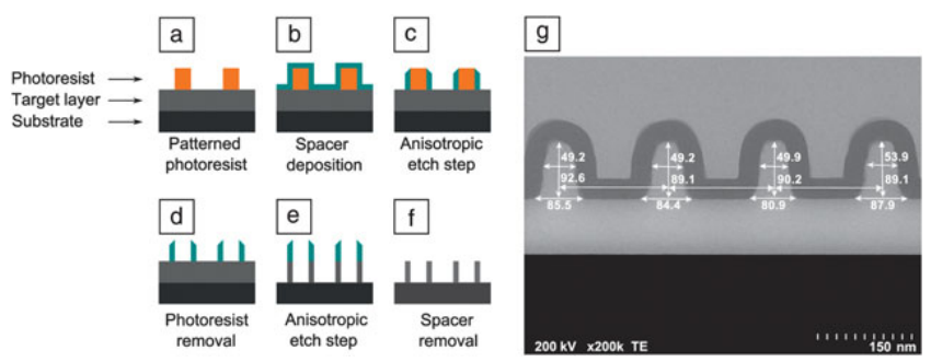
Thermal oxidation of Si at temperatures > 800 °C yields SiO2. To avoid such high temperatures and long processing times and tune the material properties, (wet) chemical oxidation, (plasma-enhanced) chemical vapor deposition or sputtering and electron beam evaporation are also preferred methods to grow SiO2. The advantages of precise thickness control, optimal large-area uniformity, and the conformality over demanding substrate topologies of atomic layer deposition (ALD) based SiO2 films, all led to an expansion of target applications such as; spacer based self-aligned double/quadruple patterning (SADP or SAQP) in fabricating DRAM and logic chips (Link), interface engineering between Si and high-k materials (Link), moisture barrier or protective or insulator coatings (Link), nanolaminate structures with tailored optical and electronic properties (Link) and double layer surface passivation in Si photovoltaics (Link), etc. to name but a few.


Link for the image

Bis(diethylamino)silane (BDEAS) [SiH2[N(CH2CH3)2]2, also known as SAM-24[MP1] , is one of the most preferred Si precursors for ALD of SiO2 and other Si-containing films. It’s an air-sensitive, moisture-sensitive, flammable, colorless, and odorless liquid precursor (boiling point 70 °C (30mm), density 0.804), which exhibits a high vapor pressure, i.e. ~100 Torr at 100 °C.

The research group of Prof. W. M. M. Kessels, Department of Applied Physics, Eindhoven University of Technology, has reported that BDEAS is suited for low-temperature synthesis of high-quality SiO2 by ALD with the SiO2 properties being relatively insensitive to the substrate temperature for the temperature range of 100 – 300 °C; for temperatures reaching 400 °C thermal stability issues of the precursor and its ligands start to play a role. The process is also relatively fast as it combines a high growth-per-cycle (0.8 – 1.7 Å/cycle) with relatively short dosing and purge times. The ALD SiO2 processes with BDEAS precursors are therefore of interest for high-volume manufacturing applications, for instance, using ALD batch processes or inline (plasma) ALD equipment.

Link for the image

Strem Chemicals, Inc., a high purity specialty chemicals manufacturer and supplier, headquartered in Newburyport, Massachusetts, USA, boasts a vast variety of ALD/CVD precursors, including BDEAS for depositing Si-based films in different applications.

Since 1964, Strem Chemicals, Inc. has been serving its clients from academic, industrial, and government research and development laboratories as well as commercial scale businesses in the pharmaceutical, microelectronic, and chemical/petrochemical industries. Strem also provides custom synthesis (including high-pressure synthesis) and current good manufacturing practice (cGMP) services. With ISO 9001 certification for the Quality Management System (QMS) standard and documentation, Strem products are high purity materials, typically 99%, with some at 99.9999% metals purity. Strem utilizes a comprehensive range of analytical techniques tailored to each product to ensure quality because  researchers typically rely on the supplier's quality procedures and documentation, which if poorly conducted[MP1]  may kill a great research idea. All of Strem's catalogs, since inception, have listed “Color and Form” for every product as primary indicators of quality.


 [MP1]SAM-24 may be an Air liquide trademark.

----------

Promotional blog written and researched by Abhishekkumar Thakur and Jonas Sundqvist, BALD Engineering AB

Tuesday, July 28, 2020

Sales to 300 mm wafer market boosts Picosun to new record in Q2/2020

ESPOO, Finland, 28th July 2020 – Picosun Group, leading supplier of AGILE ALD® (Atomic Layer Deposition) thin film coating equipment and solutions, reports record sales during the second quarter of 2020. Especially the Group’s 300 mm production ALD technology was well welcomed by customers.

Total order intake in the second quarter of 2020 was 11,6 M€ and total net sales 9,8 M€. Picosun’s first quarter of 2020 was also successful. Order intake during the first half of the year was 22,3 M€ which resulted in 137% growth compared to the same period last year, and net sales was 20,5 M€, resulting in 51% growth.


Photonics market, including applications in lighting, optoelectronics, displays and sensors, was one of the key drivers behind Picosun’s growth. Picosun has dedicated a lot of work to developing turn-key industrial ALD solutions specifically for wafer sizes up to 200 mm. Photonics, sensor and lighting device manufacturers typically operate on these wafer sizes, and Picosun’s solutions have been sought after amongst these industries. Picosun has also entered the 300 mm production ALD market and has received first pilot orders for its novel 300 mm manufacturing solutions.

“I am very pleased of this excellent growth during the first half of 2020. We have managed well, even despite the challenges caused by the coronavirus outbreak earlier in the spring, and our customers have trust on us. We are happy to report several return customers as well as various multiple ALD system sales to the same customer. Our strategy to focus on industrial customers and large scale manufacturing is bearing fruit and interest towards our production ALD solutions is booming. Development and optimization of novel manufacturing ALD technologies for even bigger markets is proceeding and we are eagerly waiting to launch these disruptive solutions to the public later this year,” states Mr. Jussi Rautee, CEO of Picosun Group.

Friday, July 17, 2020

Atomic Layer Etch Expands To New Markets - AVS ALE2020 report

Mark Lapedus reports in SemiEngineering that is expanding to new markets as presented at the recent AVS ALE2020 Virtual conference.

At the conference companies, R&D organizations and universities presented papers on what’s next in ALE. They include:
  • Plasma ALE, which performs directional etches (anisotropic), is in production and expanding into applications beyond traditional silicon, such as gallium-nitride (GaN) and refractory metals.
  • Thermal ALE, which performs unidirectional etches (isotropic), is still in its infancy. Some are targeting thermal ALE for next-generation transistors.
  • The University of Colorado presented work on thermal ALE for metal gates, dielectrics, among others.
  • The University of Delaware presented some work on thermal ALE for metals and alloys. Others are also developing the technology.

According to Risto Puhakka, President at VLSI Research, within the overall etch market, ALE is still small, representing a “few hundred million dollar” business, according to VLSI Research. Applied, Lam and TEL are the major ALE players. Hitachi, Oxford and others compete here.

Judging by other informations known to BALD Engineering also PlasmaTherm is in the ALE market and ASM International has active R&D in ALE (Patent: https://patents.google.com/patent/US9735024B2/en). Additional OEMs can be found by understanding the active IP filing in ALE.

The top IP filing OEMs include:

LAM Research Corp.
Tokyo Electron Ltd.
ASM IP Holding BV
Applied Materials Inc.
Beijing Naura Microelectronics Equipment Co. Ltd.
Multibeam Corp.
Oxford Instruments Nanotechnology Tools Ltd.
Picosun OY

The top filing IDMs/Foundries include:

Taiwan Semiconductor MFG Co. Ltd.
IBM
Samsung Electronics Co. Ltd.
Intel Corp.
Globalfoundries Inc.
Micron Technology Inc.
Sandisk Technologies LLC

Source:
Atomic Layer Etch Expands To New Markets LINK


The Patbase ALE clustered IP family tree allows you to click and zoom in on a cluster and zoom in further to nodes (sub-clusters). 172 documents (families) have been selected (contain appropriate data), and are contain in these clusters. As can be see the ALE families overlap a lot with Atomic Layer Deposition Keyword clusters (Provided by TECHCET).