Wednesday, April 16, 2025

ASML Posts Strong Q1 2025 Results Amid AI-Driven Demand and Tariff Uncertainty

ASML kicked off 2025 with solid first-quarter performance, beating expectations on both earnings and revenue as demand for advanced lithography tools—driven by AI and next-generation semiconductor nodes—remained robust. While the company reaffirmed its growth outlook for 2025 and 2026, it also flagged increasing geopolitical uncertainty, particularly around US-China tariffs, as a risk factor for the months ahead.

ASML delivered strong Q1 2025 results, with earnings per share of $6.82 and revenue of $8.80 billion, reflecting a 56% year-over-year increase. The company met or exceeded guidance across major financial metrics, with gross margins at 54%, supported by favorable EUV system configurations and higher average selling prices. Net system sales reached €5.7 billion—€3.2 billion from EUV and €2.5 billion from non-EUV—while Installed Base Management sales added €2 billion. Bookings totaled €3.9 billion, mostly from logic customers. Despite a seasonal dip in free cash flow due to payment timing and capital investments, ASML remains financially strong with €9.1 billion in cash.


CEO Christophe Fouquet and CFO Roger Dassen emphasized the ongoing strength of AI as a demand driver, particularly in advanced logic and memory, while acknowledging growing macroeconomic and geopolitical uncertainties—especially around tariffs. They reiterated revenue expectations for 2025 between €30 billion and €35 billion, with 2026 also anticipated to be a growth year. However, they cautioned that new tariff dynamics introduce significant unknowns for both ASML and its customers, which may affect gross margins and the broader supply chain.


On the technology front, ASML made progress with both its Low NA and High NA EUV systems. The NXE:3800E tool is now shipping at full spec and is seeing strong adoption among logic and memory customers aiming for single-expose EUV. Meanwhile, the High NA NXE:5000 has demonstrated better maturity compared to the Low NA at a similar stage, with customers like Intel and Samsung reporting substantial gains in productivity and process simplification. ASML shipped its fifth NXE:5000 in Q1 and is beginning shipments of the NXE:5200, which will be critical for phase two customer evaluations. Full-scale adoption is expected from 2026–2028, contributing to ASML’s long-term revenue forecast of €44 billion to €60 billion by 2030.

ASML addressed growing concerns over US and China tariffs, highlighting the high level of uncertainty surrounding their scope and impact. The company is actively assessing both direct and indirect consequences, including tariffs on system sales, parts imports, and servicing operations. ASML emphasized that it is working closely with customers and suppliers to mitigate disruptions and ensure that tariff-related costs are fairly distributed across the value chain, rather than being absorbed solely by ASML. While management acknowledged that these discussions are still evolving and outcomes remain unclear, they cautioned that tariffs could introduce volatility in margins, supply chain planning, and customer delivery schedules. Despite this, ASML noted that the current business conversations with customers remain unchanged and the long-term strategic investment momentum—especially in logic and AI-related capacity—appears resilient.

Sources:

ASML Holding N.V. 2025 Q1 - Results - Earnings Call Presentation (NASDAQ:ASML) | Seeking Alpha

ASML Holding N.V. (ASML) Q1 2025 Earnings Call Transcript | Seeking Alpha

Applied Materials Unveils Industry-First Ruthenium-Cobalt Liner and Next-Gen Dielectrics to Enable 2nm Chip Wiring and Boost 3D Stacking for Energy-Efficient AI Computing

Applied Materials has announced new materials engineering breakthroughs aimed at improving energy efficiency in computing by enabling copper wiring to scale down to the 2nm node and beyond. Central to this innovation is the industry’s first high-volume use of ruthenium in a binary metal liner with cobalt (RuCo), which allows for thinner liners, improved copper fill, and up to 25% lower electrical resistance. This innovation, part of the new Endura™ Copper Barrier Seed IMS™ system, combines six process technologies in one high-vacuum system and is already being adopted by major logic chipmakers. These advances address the increasing challenges of interconnect resistance and mechanical weakness as chip feature sizes shrink.


Applied Materials’ new Endura™ Copper Barrier Seed IMS™ with Volta™ Ruthenium CVD combines six different technologies in one high-vacuum system, including an industry-first combination of materials that enables chipmakers to scale copper wiring to the 2nm node and beyond.

Complementing this, Applied also introduced an enhanced version of its long-standing Black Diamond™ low-k dielectric material, designed to reduce capacitance and reinforce chip strength — critical for advanced 3D stacking in logic and memory chips. These solutions help overcome scaling limitations associated with Moore’s Law and are critical for sustaining AI-driven computing advancements. As demand for high-performance, energy-efficient chips grows, Applied’s innovations are expanding its served market for interconnect technologies, which is projected to reach $7 billion per 100K wafer starts per month with the addition of backside power delivery.


With the semiconductor industry’s first use of ruthenium in high-volume production, Applied Materials' new binary metal combination of ruthenium and cobalt (RuCo) enables copper chip wiring to be scaled to the 2nm node and beyond and reduces electrical line resistance by as much as 25 percent.


Applied Materials today introduced an enhanced version of the company’s Producer™ Black Diamond™ PECVD dielectric film. This new material enables chip scaling to 2nm and below, while offering increased mechanical strength to help take 3D logic and memory stacking to new heights.


The new Producer™ Enhanced Black Diamond™ dielectric is a revolutionary product, enabling next-generation chips of the AI era. Enhanced Black Diamond™ addresses two key issues in leading-edge chips. As wires become closer together, parasitic capacitance increases. The phenomenon slows signals down, worsening performance and energy consumption. Additionally, damaging plasma manufacturing processes can cause the thinner insulating dielectric material between wires to fracture or collapse, potentially leading to chip failure (Embedded from Youtube : https://youtu.be/uJju9KNA-yE?si=ae-Eqc0Qaf5J8e0W).

Sources:


Photos accompanying this announcement are available at


Saturday, April 12, 2025

Neumonda and Ferroelectric Memory Company Collaborate in the Commercialization of Non-Volatile DRAM

Neumonda and Ferroelectric Memory (FMC) are working together to design, provide test solutions, and market FMC’s nonvolatile DRAM+. This collaboration aims nothing less than to bring semiconductor DRAM memory design and manufacturing back to Germany.


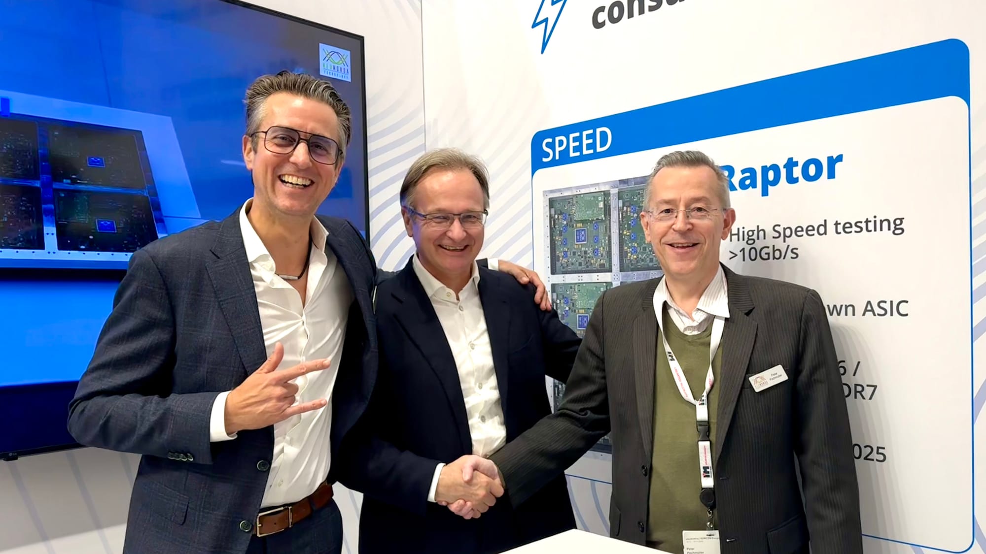
Marco Mezger, COO of Neumonda, Thomas Rueckes, CEO of FMC, and Peter Poechmueller, CEO of Neumonda (from left to right), celebrate the collaboration of the two German memory powerhouses


Two German memory innovators join forces to bring semiconductor memory back to Germany

Bad Homburg / Dresden, April 3, 2024 – Neumonda and Ferroelectric Memory (FMC) are working together in the design, provision of test solutions, and marketing of FMC’s nonvolatile DRAM+. This collaboration aims nothing less than to bring semiconductor DRAM memory design and manufacturing back to Germany.

FMC commercializes a disruptive technology that combines non-volatile properties of ferroelectric hafnium oxide (HfO2) with RAM to create a non-volatile DRAM memory for AI, medical, industrial, automotive, and consumer applications. As part of the agreement, Neumonda which holds several patents in the design and testing of DRAM memory, will support FMC with memory consulting services and with its Rhinoe, Octopus, and Raptor test platforms for FMC’s nonvolatile DRAM+ products.

“FMC was founded to exploit the disruptive invention of the ferroelectric effect of HfO2 for semiconductor memories. Applied to a DRAM, it turns the DRAM capacitor into a low power, nonvolatile storage device while maintaining the high DRAM performance to produce a disruptive nonvolatile DRAM memory ideal for AI compute,” explained Thomas Rueckes, CEO of FMC. “Since our technology is unique in the market, cost-effective testing of our memory products is of great importance for our product offerings. With Neumonda and its radically new approach to testing, we have found a partner that can help us speed up the development of our products. We also are excited to work with Neumonda as we share the common vision to bring Memory back to Europe”

Neumonda combines unmatched expertise in memory and, with its Neumonda Technology division, revolutionizes memory testing. Its testers are lightweight, low-cost, and energy-efficient and enable Neumonda to conduct manufacturer-independent tests at a level and detail that has not been possible before—all this at a fraction of the costs of traditional testers.

“As our test platforms are maturing, FMC’s products are an ideal test ground to prove the capabilities of our Rhinoe, Octopus, and Raptor testers, as well as the high-quality yield they enable,” explained Peter Poechmueller, CEO of Neumonda. “One of my personal goals behind founding Neumonda was to bring semiconductor memory back to Europe. With this collaboration, we take a big step closer to establishing a new German memory manufacturer.

About FMC

FMC was founded in 2016 as a spin-off from NaMLab GmbH, a TU Dresden company, to commercialize ferroelectric hafnium oxide technology originally invented by Qimonda, the former German DRAM manufacturer. FMC is a full stack fabless semiconductor company with operations in Dresden (Germany), Milan (Italy) and North America. FMC product offerings include high density, low power, nonvolatile DRAM and Cache chiplets for disruptive performance and power efficiency improvements in edge and cloud AI systems. Since its foundation, FMC has been working closely with Saxonian, Federal German and European funding providers and is very thankful for this continuous support. For more information visit: www.ferrolectric-memory.com

About Neumonda

NEUMONDA combines extensive memory experience with the “DNA” of former memory manufacturer Qimonda, with the aim to offer the most extensive portfolio of specialized memory solutions and competence in the market. It governs MEMPHIS Electronic, a distributor of memory ICs and modules of different suppliers; Intelligent Memory, the manufacturer of DRAM and NAND-based memory solutions; and NEUMONDA Technology which designs and holds IP for application test systems for memory applications. Combining these different areas of expertise, NEUMONDA is able to offer unique global memory competency that can help companies in any industry to meet their current and future memory requirements. www.neumonda.com

Thursday, April 10, 2025

AlixLabs to Demonstrate APS™ on 300-millimeter UMC wafers at the 2025 CMC Conference

Atomic Layer Etching Pitch Splitting (APS) proven on more industry-leading wafers, doubling fin density and proving flexibility without EUV.

Austin, TX, USA/Stockholm, Sweden – April 10th, 2025 – AlixLabs AB, a Swedish semiconductor startup specializing in Atomic Layer Etching (ALE), today demonstrates the latest in its line of groundbreaking development in advanced chip fabrication unveiling additional research into its novel semiconductor manufacturing process known as APS™ (Atomic Layer Etching Pitch Splitting) capable of doubling fin density while introducing the unprecedented flexibility to vary pitch and critical dimensions within the same wafer area.


Proven on 300-millimeter wafers provided by United Microelectronics Corporation (UMC), the APS™ technology successfully halved pitch compared to current industry benchmarks. This significant advancement was achieved entirely without relying on expensive and energy-intensive Extreme Ultraviolet (EUV) lithography.

Instead, APS™ leverages advanced etching techniques that substantially enhance sustainability, drastically reducing energy consumption without compromising throughput. Previous demonstrations of the APS™ process, validated through Intel’s Test Vehicle Program[1], confirmed its potential by achieving metal pitches as small as 25 nanometers.


“Today we are sharing more proof that the APS™ process can be a game changer for leading foundries. Thanks to UMC, we have been able to verify our process on production wafers that are shipped in quantities measured in millions of wafers annually,” said Dr. Robin Athle, Principal Researcher at AlixLabs. “Our mission is to create equipment that allows companies that don’t have access to EUV tools to scale down their production to 5 nanometer and beyond. By eliminating the dependency on EUV lithography, we are offering the industry a path towards more sustainable and economically feasible high-density chip production.”

Detailed results from AlixLabs’ UMC wafer tests and further insights into APS™ technology will be presented at the 2025 CMC Conference, scheduled for April 10th in Austin, Texas. Dr. Athle’s presentation “Atomic Layer Etching Pitch Splitting (APS™): a New Alternative to Multi Patterning” will be held at 4:00 PM at the Bergstrom Ballroom in Hilton Austin Airport Hotel.

Sunday, April 6, 2025

IBM and Tokyo Electron Extend Strategic Partnership to Advance Chiplet Architectures and High NA EUV for Generative AI Era

IBM and Tokyo Electron (TEL) have renewed their long-standing semiconductor research partnership with a new five-year agreement focused on advancing next-generation semiconductor nodes and chiplet architectures tailored for the demands of generative AI. Building on more than 20 years of collaboration, the companies aim to leverage their complementary strengths—IBM’s semiconductor process integration and TEL’s advanced manufacturing equipment—to develop breakthroughs in performance and energy efficiency, including new approaches to 3D chip stacking and patterning with High NA EUV lithography.

"IBM and Tokyo Electron have built a strong relationship of trust and innovation through years of joint development. We are excited to continue to build on our long-standing partnership with IBM for another five years. This renewed agreement underscores our mutual commitment to advancing semiconductor technologies, including patterning processes with High NA EUV." said Toshiki Kawai, Representative Director, President & CEO Tokyo Electron Limited. "Our collaboration at the has been instrumental in driving innovation, and we look forward to continuing this journey together."

The partnership is anchored at the Albany NanoTech Complex, a world-leading semiconductor R&D ecosystem operated by NY CREATES. This collaboration has already played a key role in positioning the site as the National Semiconductor Technology Center’s EUV Accelerator. IBM and TEL will continue joint research at Albany, accelerating U.S. leadership in chip innovation and enabling critical infrastructure for the generative AI era.

Company Summaries:
Tokyo Electron (Japan): A global leader in semiconductor production equipment, specializing in lithography, etch, and deposition systems.
IBM (U.S.): A technology and research powerhouse with deep expertise in semiconductor design, AI, and hybrid cloud infrastructure.

Sources:

Semiconductor Equipment Not Listed in Tariff Exemptions and EU and Japanese Suppliers Show Market Resilience

As of April 6, 2025, semiconductor equipment is not explicitly included in the list of exempted products under the U.S. tariffs detailed in Annex II of President Donald Trump’s executive order. While semiconductors and electronic components such as integrated circuits and diodes are covered, the exemption does not extend to manufacturing equipment.


Since the April 2, 2025 tariff announcement, ASML’s stock fell about 9.5%, showing more resilience than the Philadelphia Semiconductor Index (SOX), which dropped approximately 16.7% (deepest point).

Semiconductor equipment not listed in tariff exemptions, but EU and Japanese suppliers show market resilience

Despite this, European and Japanese semiconductor equipment companies have shown relative resilience in the wake of the April 2 tariff announcement. ASML, the Netherlands-based manufacturer of advanced lithography tools, saw its stock fall by about 9.5 percent, compared to a sharper 16.7 percent drop at the lowest point for the Philadelphia Semiconductor Index (SOX). This suggests continued investor confidence in ASML’s position and the essential nature of its equipment in semiconductor manufacturing.


Other global equipment firms also experienced moderate declines. ASM International, also from the Netherlands, saw an 8.3 percent drop. Tokyo Electron, Japan’s leading chip tool supplier, declined by 8.1 percent. In contrast, US-based companies faced more significant losses: Applied Materials dropped 14.1 percent, Lam Research fell 19.9 percent, and KLA Corporation declined by 16 percent between April 2 and April 4.

The broader tariff policy applies a 10 percent baseline rate on most imports starting April 5, with higher rates—up to 50 percent—for goods from 83 countries (including EU members) beginning April 9. Annex II outlines exemptions across multiple sectors: critical minerals, pharmaceuticals, energy products, integrated circuits, and fertilizers. However, semiconductor manufacturing equipment is not among the listed exemptions, indicating it remains subject to the new tariffs unless otherwise specified in future regulatory clarifications.

Despite this, the muted market response for EU and Japanese equipment makers highlights their global significance and the likelihood that US firms will continue to source vital tools from these suppliers, tariffs notwithstanding.

Background:

Starting on April 5, a 10% baseline tariff will be applied to nearly all products from all countries, with a few notable exceptions explained later. The executive order’s Annex I lists 57 countries (83 when accounting for all European Union member states) that will face higher tariffs of up to 50%, which go into effect on April 9. The new tariffs will stack on previous product-specific tariff rates. As a reminder, a tariff is a tax paid at the border by an importer seeking to bring products into the United States from a foreign country.

The exempted items in Annex II include, but are not limited to: copper, pharmaceuticals, semiconductors, lumber articles, certain critical minerals, energy/energy products, and products facing section 232 tariffs from the current administration (steel, aluminum, automobiles and any future section 232 investigations). While some of these industries were exempted due to their important roles in the economy (energy and critical minerals), others were excluded as they are a target for future restrictions (copper, lumber, pharmaceuticals and semiconductors).

Annex II lists a range of products exempted from trade actions, categorized across several sectors. It includes critical minerals and ores, such as copper, cobalt, lithium, tungsten, manganese, rare-earth elements, and graphite.

It also covers a wide array of chemicals and industrial compounds, including hydrofluoric acid, titanium dioxide, aluminum oxide, and various oxides, chlorides, and sulfates.

A significant portion of the list includes energy products, such as crude oil, natural gas (liquefied and gaseous), coal, petroleum derivatives, lubricants, and electricity.

The Annex lists several electronic components, including integrated circuits (processors, memory, amplifiers, other ICs), semiconductor devices (diodes, transistors, thyristors, optical isolators), and parts for these devices.
In agriculture, exempted products include fertilizers containing potash and NPK compounds, peat, and veterinary vaccines.

The document also includes many pharmaceuticals and medical products, such as antibiotics, hormones, vitamins, vaccines, and active pharmaceutical ingredients (APIs), along with cell therapy products and clinical trial materials.

There are exemptions for polymers and plastics in primary forms, including polyethylene, polypropylene, PTFE, silicones, and epoxide resins.


Additionally, doped materials for electronics, such as silicon wafers (HTS 38180000), and pigments and colorants like titanium dioxide and copper phthalocyanine, are listed.


Saturday, April 5, 2025

BALD Engineering - Semiconductor & Strategic Tech Weekly Summary

Tariffs, Trade & Supply Chain Disruptions

Despite the US exempting semiconductors from new tariffs, chip stocks plunged, dragging the Nasdaq Composite into a deeper correction—now down over 20% since December. Major players like Marvell, ON Semiconductor, Broadcom, and Microchip posted double-digit losses, while Nvidia and Micron also fell sharply, erasing much of their recent gains. The Philadelphia Semiconductor Index (SOX) dropped 7.6% in a single day, marking its lowest point since November 2023.


Adding to the pressure, China retaliated with a sweeping 34% tariff on all US imports, while concerns mount over broader supply chain disruptions.

Tariff Reality Check: The Taiwan Dependency
While most semiconductors are manufactured in Taiwan, relocating chip production to the US offers limited tariff relief. Even if chips are fabricated in the US, they often must return to Taiwan for testing and packaging, stages still dominated by Taiwanese subcontractors.

From Semiconductor supply chain by Calus Aasholm, subscribe to his blog here: https://lnkd.in/d2ZXMHjw

Claus Aasholm points out that, even if test and assembly were moved, final packaged chips are still sent back to Taiwan to be integrated into devices like phones, PCs, and servers. Moreover, the bulk of materials used across the value chain still come from outside the US.

Given these realities, and in light of unpredictable tariff policies, manufacturing outside the US currently remains more cost-effective and reliable. Notably, the Taiwan-specific tariffs could hurt US firms the most, as Taiwan leads in semiconductor design and in key product segments like PCs, servers, and smartphones.

Apple, heavily dependent on Southeast Asia for production, also declined 7.3%. Sub-equipment providers like MKS Instruments and Advanced Energy suffered proportionally steep losses before markets closed for the weekend.


Technology Leadership & Industry Momentum - Ångström Era Has Arrived

At its Vision 2025 conference, Intel announced that its 18A (1.8nm) process node has officially entered risk production, marking a major milestone in its “five nodes in four years” roadmap set to reclaim tech leadership from TSMC. According to Intel’s Kevin O’Buckley, 18A will be the first node to feature RibbonFET gate-all-around transistors and PowerVia backside power delivery.

Intel is also progressing toward its 14A node, leveraging High-NA EUV lithography, representing a leap in scaling capability.

In parallel, Intel is bringing high-volume 3nm chip production to Europe in 2025 through Fab 34 in Leixlip, Ireland. This facility will support Xeon 6 server chips and expand Intel Foundry Services’ offerings in Europe—part of Intel’s push to localize and diversify its global footprint.


Critical Materials, Tariffs & European Innovation

Looking ahead, the Critical Materials Council (CMC2025) summit kicks off next week in Austin, Texas, at a moment of intensified scrutiny on material dependencies. On April 2, the US imposed 10–50% tariffs on a broad array of semiconductor-enabling materials, many of which the US is a net importer of. The list includes:

1️⃣ Specialty Gases and Etchants

  • Neon [Ne], Krypton [Kr], Xenon [Xe]

  • Nitrogen trifluoride [NF₃], Hexafluorodisilane [Si₂F₆]

  • Sulfur hexafluoride [SF₆], Carbon tetrafluoride [CF₄], Octafluorocyclobutane [C₄F₈], Trifluoromethane [CHF₃]

  • Fluorinated silanes, Ultra-pure hydrogen [H₂]

2️⃣ High-Purity Metals and Elements

  • Gallium [Ga], Indium [In], Germanium [Ge]

  • Tantalum [Ta], Niobium [Nb], Hafnium [Hf], …

3️⃣ Rare Earth Elements (REEs)

  • Yttrium [Y], Terbium [Tb], Dysprosium [Dy]

  • Neodymium [Nd], Lanthanum [La], Cerium [Ce]

  • Praseodymium [Pr], Samarium [Sm], Europium [Eu], Gadolinium [Gd], Scandium [Sc]

4️⃣ Semiconductor Substrates and Wafers

  • Monocrystalline silicon wafers (300mm), Silicon-on-insulator wafers [SOI]

  • Silicon carbide [SiC], Sapphire [Al₂O₃], Gallium nitride [GaN], Gallium arsenide [GaAs], Indium phosphide [InP]

5️⃣ Photoresists and Lithography Materials

  • EUV photoresists, Chemically amplified resists (CARs)

  • KrF and ArF excimer laser gas blends

6️⃣ CMP and Wet Process Materials

  • Colloidal ceria, High-purity alumina slurries, High-purity silica [SiO₂]

  • Advanced CMP slurries and pads, Rare-earth-based slurries

7️⃣ CVD/ALD Precursors

  • Trimethylaluminum [TMA], Tetrakis(ethylmethylamino)hafnium [TEMAH], Titanium tetrachloride [TiCl₄]

  • High-purity silanes [SiH₄, TEOS], Organometallic precursors for metal gates and high-k dielectrics

Gadolinium: A Strategic Blind Spot
A glaring vulnerability emerged: gadolinium, a rare earth essential for over 30 million MRI scans annually, is almost entirely sourced and refined in China. Prices have risen over 50% since 2017, and any disruption would heavily impact GE Healthcare, Bayer, Bracco, and Guerbet—all of whom rely on it for MRI contrast agents. Yet, it remains overlooked in US trade strategies.

Swedish Tech start up GREEN14 Breakthrough in Sustainable Recovery
In Switzerland last week, GREEN14 partnered with Oerlikon for a successful testing program using DC plasma equipment to validate its multi-material hydrogen plasma process. The company demonstrated the recovery of:

✅ Copper from copper sulfide
✅ Titanium from titanium dioxide
✅ Tungsten from tungsten oxide
✅ Aluminium from aluminium oxide

This progress confirms the scalability of GREEN14’s clean tech process, unlocking new sustainable pathways to critical raw materials beyond silicon. It supports Europe’s push toward resilience, emissions reduction, and strategic material independence.