Wednesday, December 9, 2020

Two days of Particle Atomic Layer Deposition and advanced surface engineering technique

ALD to take over more and more as CVD and spin-on processes no longer are viable for 3D NAND

EE Times reports [LINK] about the recently announced Striker FE from Lam Research, an enhanced atomic layer deposition (ALD) platform addresses semiconductor manufacturing challenges for 3D NAND as well as DRAM. It employs advanced dielectric gapfill technology the company has dubbed “ICEFill” for filling 3D NAND and DRAM structures — as well as logic devices — in emerging nodes. 


Lam Research’s recently announced Striker FE enhanced atomic layer deposition (ALD) platform addresses semiconductor manufacturing challenges for 3D NAND as well as DRAM
Lam Research Striker FE - Key applications (LINK):
  • Gapfill dielectrics
  • Conformal liners
  • Patterning spacers and masks
  • Hermetic encapsulation
  • Etch stop layers
  • Optical films
The need for gapfill methods isn’t new, said Aaron Fellis, vice president and general manager of Dielectric ALD products, but the traditional ones no longer meet today’s needs, especially as 3D NAND is stacked higher. “They’re so tall and they have a number of different features that get etched through them to enable the integration of different steps,” he said. “Ultimately, they need to get filled back up with a dielectric material, most commonly silicon oxide.”


Legacy techniques, such as chemical vapor deposition, diffusion/furnace, and spin-on processes that are normally used as gapfill for semiconductor manufacturing are no longer viable for 3D NAND, Fellis said, due to trade-offs between quality, shrinkage, and gapfill voids. “They tend to shrink and distort the actual structure that the customer is building and designing.”

According to Risto Puhakka, president of VLSIresearch, Lam Research is a dominant player for ALD technology, and the demands of its technology reflect those placed on memory. It’s all about increasing density for applications, such as artificial intelligence, that require more bits while keeping costs the same, and that includes gapfill capabilities as the memories such as 3D NAND are stacked higher, he said. “The stacking becomes more and more challenging from the manufacturing perspective, but the chip makers themselves get it a little bit little anxious about how much they have to spend.” Sticking with a known material such as silicon oxide adds some predictability because it’s well understood

But just as 3D NAND stacking will eventually hit limits, so will the gapfill techniques and ALD technology, added Puhakka. “It has its own roadmap and limitations.”

Monday, December 7, 2020

Chipmetrics Oy commercialises 3D test chip for ALD developed by VTT

The PillarHall test chip for analysing 3D thin film structures is ready for market. Chipmetrics Oy, a spin-off of VTT, is now starting to commercialise the solution. The test chip enables the production of smaller nanostructures and components. This opens up new opportunities for the development of semiconductors, memory circuits and smart devices, among others.


3D manufacturing and integration are megatrends in the semiconductor industry, as they can be used to improve the performance and energy efficiency of transistors and memory circuits. New micro-scale structures and materials as well as shrinking geometry are challenges for semiconductor manufacturers because they require process equipment, measurement and testing developed for 3D. PillarHall is the solution to these challenges.

Large global market

Artificial intelligence is being integrated everywhere, and intelligent transport, data centres and medical technology, among others, are affecting on people's lives. Components are now required to be more reliable than ever before, and more measurement and testing is needed to this end. The PillarHall test chip is suitable for the reliable, fast and cost-effective comparison of manufacturing processes of thin film structures. It can be used to measure the conformality of the thin film process, i.e. the ability to coat a 3D object evenly. 

"The PillarHall disposable test chip can be used to compare different 3D thin film processes and reactors. The method is exceptional, as typically measurements have been made directly from the processed wafers using demanding and expensive measuring devices. The test chip can be used to accelerate process development and also monitor production in the future,” says Chipmetrics founder, Dr. Mikko Utriainen.

"VTT has patented the unique structure of the test chip and developed manufacturing methods for the production of test chips. This provides a good technological basis for the growth of Chipmetrics in the global market,” says Tauno Vähä-Heikkilä, Vice President of Microelectronics, VTT.

Manufacturing to continue at Micronova

The test chip is the result of deep technological expertise: its background is the leading-edge research in atomic layer deposition (ALD) in Finland and VTT's experience in MEMS manufacturing processes. The test chip has been developed by VTT through various research projects since 2013. The development has taken place at Micronova, a unique, collaborative research, development and production environment that combines research and industry. In addition to VTT and Aalto University, some 20 companies operate in Micronova.

"With my experience in business development at VTT and 14 Research to Business projects, I am familiar with the challenges of a research-oriented start-up for an academic entrepreneur. PillarHall’s journey has so far been exceptionally successful in many ways. Its unique business model and product, market, demand, customer feedback, sales channels and scalability are all very promising,” says Utriainen.

The initial market focus of the test chip is in ALD. In addition to ALD equipment and process developers, component manufacturers have shown great interest in the test chip. The solution can also be used to develop any other thin film process technology to meet 3D requirements. 

VTT has already piloted the test chip on the international market. The commercialisation of this technology will further boost development, and Chipmetrics indeed aims to create a global business. ALD technology is widely used in many high-tech sectors. The PillarHall test chip is an important demonstration of Finland's strong expertise in ALD, and it strengthens our position in the areas of application of this technology.

High-quality HfS2 2D-material by ALD at 100°C

Thursday, December 3, 2020

AtomicLimits launch picture database for Atomic Level Processing

AtomicLimits Now serving the community with an image library of Atomic Scale Processing (ALD, ALE etc.) and its applications - A large and expanding set of free to use high quality images generated at TU Eindhoven


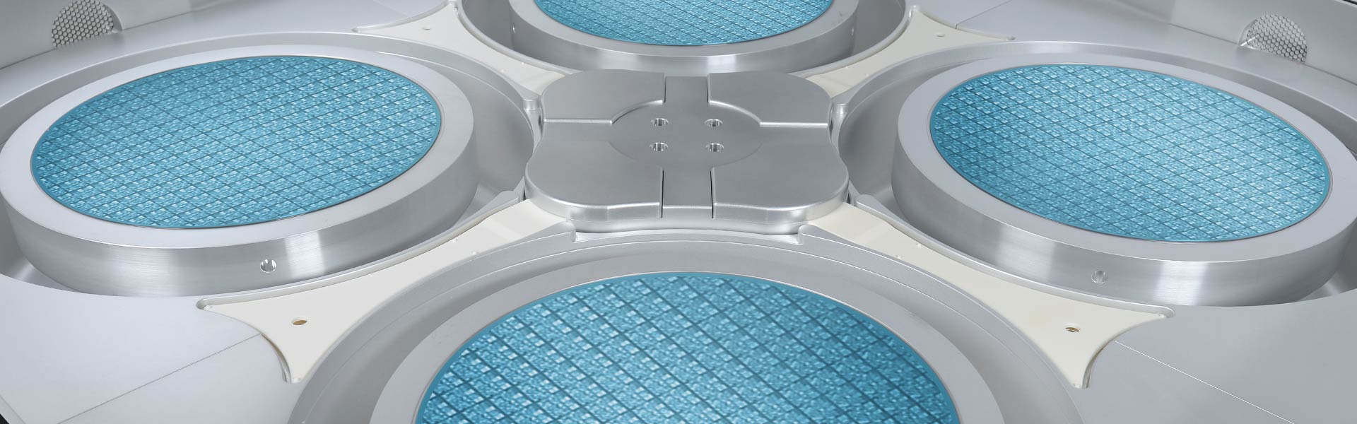
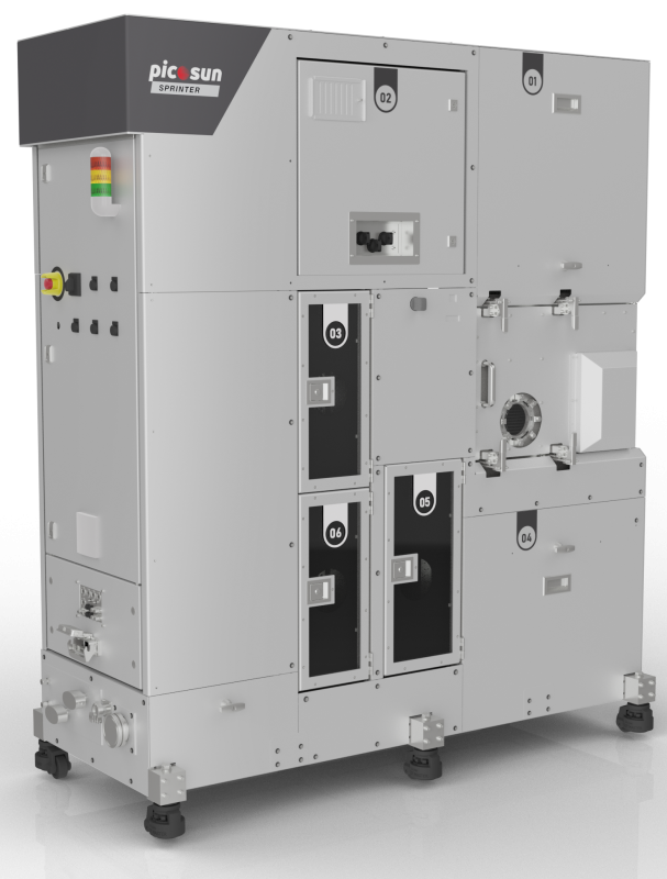
PICOSUN® Sprinter launch disrupting fast batch ALD on 300 mm wafers at EFDS ALD for Industry 2020

ESPOO, Finland, 2nd December 2020 – Picosun Group, the leading supplier of AGILE ALD® (Atomic Layer Deposition) thin film coating solutions for global industries, has launched Sprinter, a brand new, fully automated high throughput ALD production module for 300 mm wafers. Barrier, high-k and other films are deposited in Sprinter with perfect ALD for semiconductor (e.g. emerging memory, transistor, capacitor), display, and IoT component applications.


In Sprinter, single wafer film quality and uniformity are upscaled to fast batch processing with the highest reliability and repeatability(*).

Compared to vertical furnace reactors typically used for batch ALD processing, Sprinter provides higher film quality with lower thermal budget, so it is suitable also for temperature-sensitive devices.

Sprinter combines very fast process times with smaller batch sizes than in vertical furnaces, which allows greater production flexibility and minimized risk without sacrificing throughput.

The core of the Sprinter is its disruptively designed reaction chamber, where fully laminar precursor flows ensure perfect ALD deposition with no parasitic CVD growth. This minimizes the need for system maintenance.


“PICOSUN® Sprinter meets directly the challenges in high volume ALD manufacturing on 300 mm wafers. We are happy to unveil this product to our new and existing customers in 300 mm semiconductor markets, and offer them a truly disruptive, modern alternative to old technologies in batch ALD manufacturing,” says Mr. Jussi Rautee, CEO of Picosun Group.

SEMI S2/S8 certified PICOSUN® Sprinter module can be integrated to customer’s manufacturing line or cluster. It is suitable also for single wafer manufacturing lines as it does not disturb the process flow. Sprinter is run with Picosun’s new, proprietary PicoOS™ operating system and process control software.

“Together with Sprinter, we are launching also our PicoOS™ operating system. Own operating system and process control software, developed by our in-house software team, means the highest control precision and accuracy, the fastest service times, and the best reliability and quality for our customers,” continues Rautee.

Full stack PicoOS™ software allows control, operation and configuration of PICOSUN® ALD equipment – either standalone systems or full production clusters – via one unified, intuitive, and user-friendly graphical HMI and ensures smooth connection between the system and the customer’s factory automation via SECS/GEM protocol.

Sprinter is available for process demos at Picosun facilities. Sprinter module sales starts in January 2021 and full Sprinter cluster with several ALD modules, central vacuum wafer handling unit and EFEM is available later in spring 2021.

Picosun launches PicoOS™, a unified control software for PICOSUN® ALD modules and clusters

ESPOO, Finland, 2nd December 2020 – Picosun Group, leading provider of AGILE ALD® (Atomic Layer Deposition) thin film coating solutions for industrial manufacturing, presents PicoOS™, the new, full stack operating system and process control software for PICOSUN® ALD equipment.

“PicoOS™ brings PICOSUN® ALD equipment control to the modern era. It is designed for wafer fabs and industrial environments where transition to Industry 4.0 is ongoing. Data-driven PicoOS™ enables future production solutions where machine learning, artificial intelligence, internet-of-things, and other new digital inventions are utilized for optimum industrial efficiency,” says Dr. Jani Kivioja, CTO of Picosun Group.

Picosun’s proprietary PicoOS™ software combines individual ALD module, wafer handling and transfer system, and instrumentation control under one common graphical HMI (human-machine interface). This ensures easy, intuitive and user-friendly operation, maintenance, and configuration of the whole PICOSUN® ALD cluster.

PicoOS™ enables full factory integration via SECS/GEM protocol, process and system data logging down to 20 ms rate, and real-time export of all data for continuous monitoring and further analysis.

PicoOS™ operating system is specifically developed by Picosun’s own in-house software team for the company’s fully automated production ALD systems Morpher and Sprinter, and it will be implemented in all future PICOSUN® ALD tool platforms.

“PicoOS™ is designed to ensure the highest control precision and accuracy, the fastest service times, and the best user experience for our customers. Having in-house control over all features and sub-components of our PICOSUN® ALD solutions is a key part of our holistic service model,” continues Kivioja.

PicoOS™ has freely configurable and scalable editor for ALD process recipe and processing job creation and storage, and recipes can be edited or new ones created any time during the ALD system operation. Configurable user levels and safety logic, instrumentation and interlocks guarantee safe use in day-to-day operations, and allow full access for tool management in maintenance situations. Maintenance procedures are sped up by specific clean-up and maintenance sequences inbuilt in the software.

Wednesday, December 2, 2020

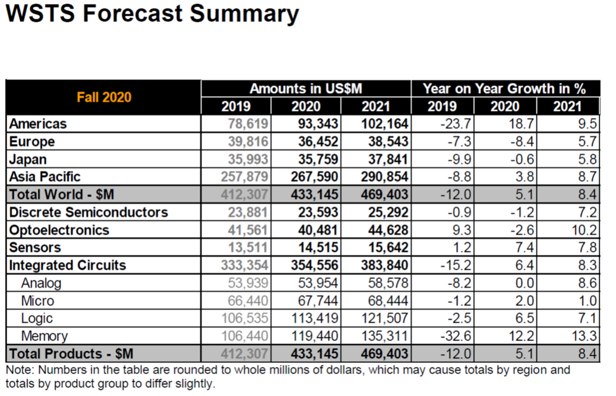
The global semiconductor market is projected to grow by 8.4 percent in 2021 according to WSTS Forecast

WSTS has released it latest forecast for the global semiconductor industry. The Worldwide Semiconductor Market is forecasted to be US$ 433 billion in 2020 - an increase of 5.1 percent from 2019- growth in all major product categories, except Optoelectronics and Discrete Semiconductors. The largest growth contributors are Memory with 12.2 percent, followed by Sensors with 7.4 percent. In 2020, Americas and Asia. Pacific regions are expected to grow.

2021, the global semiconductor market is projected to grow by 8.4 percent, driven by double-digit growth of Memory and Optoelectronics.


Saturday, November 28, 2020

SAMCO launch ALD system for MEMS and SiC and GaN power devices

Samco just released an open-load ALD system "AL-1" with a focus on gate insulator formation of GaN and SiC powerdevices, passivation layer deposition, as well as the MEMS field. This report shows the AL-1's system specifications and several pieces of performance data.

Report: Atomic Layer Deposition (ALD) System for Power Device Applications LINK


Ferroelectric Memory GmbH (FMC) Raises $20 M to Accelerate Next-Generation Memory for AI, IoT, Edge Computing, and Data Center Applications

[Press release] Ferroelectric Memory GmbH (FMC), the ferroelectric hafnium oxide technology leader, today announced that it has completed a $20 million Series B funding. The round of financing was led by the new investors M Ventures and imec.xpand, with participation of SK hynix, Robert Bosch Venture Capital, and TEL Venture Capital. The lead investor of Series A eCapital also participated in this round. The new set of investors aims to support FMC throughout the whole semiconductor value chain to bring FMC's advanced ferroelectric memory technology to market. The company plans to expand its team in Dresden, as well as to start international expansion, including into the US and Asian markets. 

"The rise of AI, IoT, Big Data, and 5G are demanding next-generation memory solutions that enable superior speed and ultra-low power consumption, while being compatible with leading-edge CMOS logic processes guaranteeing reduced manufacturing costs," said Ali Pourkeramati, CEO of FMC. "We have strong interest from customers and development partners for our advantages in fast access, program and erase speed, best-in-class ultra-low energy budget, ease-of-integration into existing manufacturing processes, and low manufacturing costs. This funding will speed up the commercialization of our ferroelectric field-effect transistor (FeFET) and capacitor (FeCAP) technology into exponentially increasing markets in the AI, IoT, embedded memory, and high-performance stand-alone data center sectors."

FMC has already made significant progress in the development of its non-volatile memory technology promising to offer superior performance compared with state-of-the-art and emerging memory solutions. It is currently working closely with major semiconductor companies, as well as with foundries in the US, Europe, and Asia. 


Transformation of amorphous hafnium oxide into its known crystalline states and into the newly discovered ferroelectric phase (Figure from www.ferroelectric-memory.com)

Technological Advantages

FMC's memory technology uses the ferroelectric properties of crystalline hafnium oxide (HfO2). HfO2 in its amorphous form is already the gate insulator material of every CMOS transistor ranging from planar to FinFET. FMC's patent-protected technology makes it simple to transform amorphous HfO2 into crystalline ferroelectric HfO2. This way, every standard CMOS transistor and capacitor can be turned into a non-volatile memory cell, a ferroelectric field-effect transistor (FeFET) or capacitor (FeCAP).

In addition to its high speed, ultra-low power, CMOS logic compatibility, reduced manufacturing cost, and extreme temperature stability, FMC's technology provides complete magnetic immunity and high radiation resistance. FeFETs and FeCAPs can be integrated into CMOS production lines using existing equipment without the need for extra capital expenditures.

About Ferroelectric Memory GmbH (FMC)

FMC has developed the most advanced ferroelectric hafnium oxide memory technology to deliver leading-edge non-volatile memory for future electronics and computing innovation. The company was incorporated in 2016 and is currently working with major semiconductor companies for its embedded and stand-alone memory solution. Its ferroelectric field-effect transistor (FeFET) and capacitor (FeCAP) technology is simple to integrate, fast, low-power, and scalable, and has high endurance with decades of data retention, suitable for a broad range of AI, IoT, edge, data center, and embedded applications.

Intel remains in the lead in 2020 semiconductor sales

IC Insights’ November shows the forecasted top-25 semiconductor suppliers in 2020. Seven top-15 semiconductor suppliers forecast to show ≥22% growth this year with Nvidia expected to post a huge 50% increase. The top-15 companies semiconductor sales are broken out into IC and O-S-D (optoelectronic, sensor, and discrete) device categories for 2019 and 2020. The forecasted 2020 top-15 semiconductor supplier ranking includes eight suppliers headquartered in the U.S., two each in South Korea, Taiwan, and Europe, and one in Japan.

Intel remains No 1. followed by Samsung and TSMC. 2020 show a very high growth for Fabless companies Qualcomm, Nvidia, MediaTek, Apple and AMD.

The Memory segment (DRAM and Flash) is led by SK Hynix +14% followed by Samsung +9% (incl. foundry) and Micron is down by -3%.

Please read the full IC Insights report here: LINK


Applied Materials will regain its No. 1 ranking in the semiconductor equipment market in 2020 from ASML

According to recent published data by The Information Network (Seeking Alpha LINK), Applied Materials will regain its top ranking in the semiconductor equipment market in 2020 from ASML. Fab equipment spend in 2020 was enhanced from pull-ins of sales into China and Taiwan, with 3Q QoQ increases of 22.5% and 36.2%, respectively.

As is well known ASML and Applied Materials does not compete in their  business segments, Lithography (ASML) resp. Deposition & Etch (Applied Materials). Applied Materials has a number 1 spot in PVD, CVD, Epi, CMP and Implant/Doping. However, business segments where Applied Materials so far has not been successful to reach a top 3 position in the past years include:
  • Atomic Layer Deposition
  • MOCVD
  • Furnace 
  • Dielectric Etch  
  • Spray Processing
  • Dielectric Etch (including ALE)
  • Wet Stations
As is known, Applied Materials have several times made very serious attempts to enter the ALD segment, but failed several times to compete with ASMI, Tokyo Electron and the South Korean OEMs (Jusung Engineering, Wonik IPS and Eugene Technology. In 2019 Applied Materials announced that it will acquire Japanese Kokusai (LINK) but the final agreement is yet not settled. If successful Applied will have an opportunity to kill 2 birds with one stone:

1. Move in to top 3 spot in ALD
2. Take number 2 spot in Furnace business


Table based on information and own assumptions in the article (Seeking Alpha LINK)

Tuesday, November 24, 2020

Beneq ALD Stories Episode 4 - The story about the BALD Engineering Blog

I
n this episode we speak to Dr. Jonas Sundqvist, founder of BALD Engineering Blog and a senior researcher and consultant of ALD/ CVD processes.

Thursday, November 19, 2020

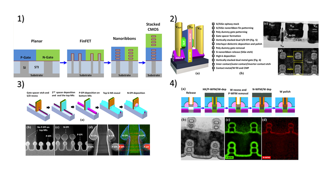
Intel to present 3D stacked Nanoribbon Transistors for Continued Moore’s Law Scaling at IEDM 2020

Intel to present stacked gate-all-around FET (GAA-FET) technology, i.e., a complementary FET (CFET) at IEDM2020. In CFETs, the idea is to stack both nFET and pFET wires on each other. A CFET could stack one nFET on top of a pFET wire, or two nFETs on top of two pFET wires. This ‘folding’ of the nFET and pFET eliminates the n-to-p separation bottleneck, reducing the cell active area footprint (LINK). Please find the announcement below:

Home-2020 - IEDM 2020 ieee-iedm.org IEDM Conference 2020. To Be Held Virtually December 12-18. The on demand portion of the conference will begin on December 5th. Intel to present 3D stacked Nanoribbon Transistors for Continued Moore’s Law Scaling: 

Stacked NMOS-on-PMOS Nanoribbons: From planar MOSFETs, to FinFETs, to gate-all-around (GAA) or nanoribbon devices, novel transistor architectures have played a critical role in driving performance predicted by Moore’s Law. Intel researchers will describe what may be the next step in that evolution: NMOS-on-PMOS transistors built from multiple self-aligned stacked nanoribbons. This architecture employs a vertically stacked dual source/drain epitaxial process and a dual metal gate fabrication process, enabling different conductive types of nanoribbons to be built so that threshold voltage adjustments can be made for both top and bottom nanoribbons. The approach combines excellent electrostatics (subthreshold slope of <75 mV/dec) and DIBL (<30mV/V for gates ≥30nm) with a path to significant cell size reduction due to the self-aligned stacking. These devices were used to build a functional CMOS inverter with well-balanced voltage transfer characteristics. (Paper #20.6, “3-D Self-Aligned Stacked NMOS-on-PMOS Nanoribbon Transistors for Continued Moore’s Law Scaling,” C.-Y. Huang et al, Intel) 

Paper #20.6, “3-D Self-Aligned Stacked NMOS-on-PMOS Nanoribbon Transistors for Continued Moore's Law Scaling,” C.-Y. Huang et al, Intel

Paper Information (IEDM 2020) : LINK

Figures from IEDM 2020 Press briefing Material -Press kit : LINK

In the images above:

·        (1) shows the evolution of transistor architectures from planar, to FinFETs, to nanoribbons and to a 3D CMOS architecture.

·        (2) (a) shows a 3D schematic diagram of stacked CMOS Si nanoribbon transistors with NMOS on PMOS, (b) describes the process flow; (c) is a TEM image of a stacked multiple-nanoribbon CMOS inverter with a 40-nm gate length and inner (Vss) and outer (Vcc) contacts, a common gate input (VIN) and an inverter output node (VOUT); while (d) is a TEM image of two Si NMOS nanoribbons atop 3 Si PMOS nanoribbons.

·       (3) (a) is a process flow of the vertically stacked dual S/D EPI process, while (b) shows P-EPI selectively grown on the bottom three nanoribbons, (c) shows N-EPI selectively grown on the top two nanoribbons, and (d) features TEM and EDS images showing selective N-EPI and P-EPI growth on the stacked nanoribbon transistors.

·       (4) (a) is a process flow of the vertically stacked dual metal gate process; (b) is a TEM image and (c, d) are EDS images of the dual metal gate with N-WFM (WFM = work function metal) on the top two nanoribbons and P-WFM on the bottom three nanoribbons.


Wednesday, November 18, 2020

Japanese researchers enable high thru put conformal CVD for SiC on Silicon wafer integration

As reported by ACS (LINK) New, concise method proposed for conformal chemical vapor deposition using sacrificial layers (SLs). SLs are porous membranes that filter high sticking-probability species, while allow the passage of low ones.

This is a really clever by researchers at University of Tokyo and IHI Corporation for CVD to compete with ALD on conformality and keeping a high deposition rate and at the same time produce bulk material like SiC on Si for larger wafer diameter.


Figure from ACS Twitter post (LINK)

Reference:

Porous Membranes as Sacrificial Layers Enabling Conformal Chemical Vapor Deposition Involving Multiple Film-Forming Species
Kohei Shima, Yuichi Funato, Noboru Sato, Yasuyuki Fukushima, Takeshi Momose, and Yukihiro Shimogaki
ACS Appl. Mater. Interfaces 2020, 12, 45, 51016–51025
Publication Date:October 30, 2020
https://doi.org/10.1021/acsami.0c14069

Tuesday, November 17, 2020

Roll-To-Roll ALD to Thermally Stabilizing NCM Cathodes for Lithium Ion Batteries

Universities in USA, China and Taiwan have developed a roll-to-roll atomic layer deposition (R2R ALD) apparatus for growing uniform thin layers of TiO2 that can be used to passivate NCM lithium battery cathode material. At a roll line speed: 2–40 mm s–1 the deposition of the TiO2was investigated. 
  • The capacity retention of TiO2-coated porous electrodes is substantially improved compared to that of the pristine cathode material for high-temperature cycling. 
  • Electrochemical impedance spectroscopy confirms that the ALD-TiO2 coating suppresses the undesired side reactions initiated at the electrode/electrolyte interface, reduces charge transfer resistance, and ultimately facilitates the Li+ transport through the composite cathode nanostructure. 
  • The NCM cathode material enables high-temperature operation (>55 °C) with enhanced specific capacity, superior rate capability, excellent cyclability, and high coulombic efficiency within a wide potential window (3.0–4.35 V). 
  • The R2R ALD technique developed in this work paves the way for large-scale fabrication of ceramic-coated cathode sheets with a production rate reaching 2.4 m min–1 for a continuous coating operation.
The schematic diagram of R2R ALD system, consisted of four main parts: gas delivering unit, sample delivering unit, plasma reactor unit, and ALD shower array unit. Figure from supporting info: https://doi.org/10.1021/acsaem.0c01541


Reference:
Roll-To-Roll Atomic Layer Deposition of Titania Nanocoating on Thermally Stabilizing Lithium Nickel Cobalt Manganese Oxide Cathodes for Lithium Ion Batteries
ACS Appl. Energy Mater. 2020, XXXX, XXX, XXX-XXX
Publication Date:November 11, 2020


New ALD Valve by TLX

TLX Pewaukee, WI, USA has developed a two-position, three-way pilot valve with performance tailored for ALD applications, including ultra-fast response, high operating temperature and compact design. According to TLX, the component used minimal power, making it more cost-effective than competing designs.

About TLX: TLX Technologies was founded in 1996 to bring to market several unique, high-speed digital valves for controlling the inflation of a vehicle air bag. During the succeeding years, TLX adapted this technology to many other markets and applications.

More information: TLX Web page LINK


AICHE 2020: Machine Learning-Based Modeling and Operation of PEALD of HfO2 Thin-Films

Here some insights from a presentation at AICHE 2020 by Yichi Zhang at UCLA entitled Machine Learning-Based Modeling and Operation of PEALD of HfO2 Thin-Films. The modelling is based on a 300 mm ASM Emerald PEALD chamber.


Forge Nano and Argonne improve yield in propylene manufacturing by ALD coating

Propylene, a precursor for commodity chemicals and plastics, is produced by propane dehydrogenation (PDH). In a PDH process, propane is selectively dehydrogenated to propylene. Production capacity via PDH is slated to grow rapidly over the next several years. The single feed/single product feature is one of the most attractive aspects of PDH, especially for propylene derivative producers looking to back-integrate for a secure and cost-effective source of propylene (IHS Markit Report LINK). 

Despite its simple chemistry, industrial implementation of PDH is very complicated owing to side reactions such as: 
  • deep dehydrogenation
  • hydrogenolysis
  • cracking
  • polymerization
  • coke formation.
According to a recent publication by Forge Nano and Argonne National Lab, an increase in PDH yield via added catalyst activity, lifetime, or selectivity represents significant energy and economic savings. 

The researchers has demonstrated that by using Pt dispersed on Al2O3 extrudate supports as a commercially relevant model system and by using atomic layer deposition (ALD) metal oxide overcoats, the metal-active sites can be tailored to increase PDH yield and selectivity. 

In the study they investigate the interplay of Pt loading, ALD overcoat thickness, and Al2O3 support surface area on PDH activity, selectivity, and catalyst stability. 

They were able to show that applying a 6–8 Å thick layer of Al2O3 on low-surface area Al2O3 supports of ∼90 m2/g surface area yields the optimal combination of stability and activity, while increasing propylene selectivity from 91 to 96%. Please find further details in the paper linked below.

Catalyst preparation method, Graphical abstract (https://doi.org/10.1021/acscatal.0c03391)


Atomic Layer Deposition Overcoating Improves Catalyst Selectivity and Longevity in Propane Dehydrogenation
Zheng Lu, Ryon W. Tracy, M. Leigh Abrams, Natalie L. Nicholls, Paul T. Barger, Tao Li, Peter C. Stair,
Arrelaine A. Dameron, Christopher P. Nicholas, and Christopher L. Marshall

ACS Catal. 2020, 10, XXX, 13957–13967
Publication Date:November 16, 2020

https://doi.org/10.1021/acscatal.0c03391

Monday, November 16, 2020

Dutch SALD and German Fraunhofer to develop Spatial ALD technology for production of 1,000 km range EV battery modules

Several reports state that Dutch SALD, a subsidiary of SoLayTec, and German Fraunhofer have jointly developed a Spatial ALD (SALD) technology for producing EV batteries that aim at 1,000 km range.
 
Not too many details are available at this point, please check SALD below for further details

SALD: LINK


From SALD Webpage: Li-ion batteries are indispensable for consumer electronics and electric vehicles, and it is vital that the safety, longevity and capacity of these batteries is maximized. Spatial ALD can assist in this. For common Li-ion batteries that comprise liquid electrolytes, ALD can be used to prepare the solid-electrolyte interphase (SEI). This artificial SEI - typically about a nanometer in thickness - protects the anode or cathode active materials (CAMs) from the electrolyte, enhancing the long-term stability and safety of the Li-ion battery.

IBM Research installs EUV tool at SUNY Poly for AI research

Albany Business Review reports that IBM Research has installed an new EUV tool at SUNY Poly in Albany, NY, USA. According to the report, the tool is part of the more than $2 billion investment from IBM Research at SUNY Poly and elsewhere to research and develop artificial intelligence technology, based on a statement given by Mukesh Khare, vice president of hybrid cloud research at IBM Research.

Full Story: LINK


SUNY Poly's Albany NanoTech Complex is the most advanced research facility of its kind at any university and includes a 300 mm Logic processing line

Friday, November 13, 2020

ALD for Industry goes digital – an interactive event with lecture program, communication, networking opportunities and after work meeting

4th Workshop, Tutorial – including digital Industrial Exhibition and Company Tour.

TOPICS:
♦ Semiconductor ♦ MEMS and Sensors ♦ Display ♦ Lightning ♦ Barriers ♦ Photovoltaics ♦ Battery ♦ Powder Coating ♦ Medical Applications ♦ Decorative Coatings

ALD for Industry provides the opportunity to get in contact with industrial and academic partners, to learn more about fundamentals of ALD technology and to get informed about recent progress in the field. The Event will focus on the current markets for ALD and addresses the applications in Semiconductor industry, MEMS & Sensors, Battery Technology, Medical, Display, Lightning, Barriers and Photovoltaics.

Web: LINK

DOWNLOAD


Tuesday, November 10, 2020

ALD and Nanotubes on Beneq ALD Stories

In Episode 3 of ALD Stories, we meet with Professor Jan Macak from the University of Pardubice. Hear and see his findings on ALD as an exceptional way to tailor the functionality of nanostructures, and the overlooked steps for making the perfect TiO2 nanotube.


Friday, November 6, 2020

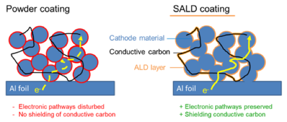
Refreshing Material Advances for Logic, Memory, and Packaging5th CMC Conference "After-Hours" Available up to December 11

How to keep semiconductor fabs supplied with critical materials despite a pandemic and trade wars was discussed by >250 industry experts gathered in virtual space October 21-22 during the 5th annual Critical Materials Council (CMC) Conference. CMC Fab Members and Associate Supplier Members were joined by leading industry analysts, educators, and investors in discussing business and technology trends in the value-chain for advanced packaging, logic, and memory. The "after-hours" virtual conversations will continue through December 11th using the conference app and website, and new people can join in through November 16th.

"There were a lot good topics especially on materials challenges for leading edge technology and heterogeneous integration, global issues on material supplies, and emerging materials development," commented Dr. Lihong Cao, Director of Engineering and Technical Marketing at ASE, and Session 4 presenter.


Dr. Lauren Link of Intel discussed the need to find ways to integrate more front-end fabrication materials into packaging. The challenge is doing so in a cost-effective manner, without over-specifying materials and process requirements.

CMC-Oregon-Header

5th Annual CMC Conference "After-hours" Starting Now!

Didn't Catch the Conference "Live"? No Worries! Register Today and Get Access to the recordings, Connect attendees, Engage in Q&A!

Registration Open until November 16

Access Presentations thru December 12

Thursday, November 5, 2020

Improving Curved uOLED encapsulation with ALD

[Beneq Blog] For the past decades, organic light emitting diodes (OLEDs) have become of great interests for applications to micro-displays. Unfortunately, these systems are highly sensitive to moisture and oxygen ingress and require high barrier encapsulation. Additionally, a specific protection needs to be added to protect the device from mechanical failure. Depending on the application, various options from glass lids to flexible barriers have been developed. The former offers high mechanical protection but suffers from long implementation processes, while the later typically exhibit low hardness and poor wear resistance.

Pinhole free encapsulation via ALD deposited directly onto micro-OLEDs means simpler manufacturing and robust protection. The thinner ALD encasement enable substrate bending and open the possibility of more compact curved devices with less complex optical engines.

Continue reading at BENEQ: LINK

Wednesday, November 4, 2020

2020 November Networking - ALD at Aalto University, Finland

When : 25.11.–26.11.2020
Where: The event will be held in Zoom
Registration : Registration period: 21.10.2020 12:00 – 11.11.2020 12:00 

2020 ALD November Networking Event page

Register here! (Without presentation DL 22.11.)

At Aalto University, many research groups' activities have a connection to atomic layer deposition (ALD). Join our public webinar and local networking event on 25.-26.11.2020. Preliminary program in this link. Registration is free but required. 

Aim: Continuing the tradition started in 2019, provide a time and place where especially local people with interest in ALD can meet and get better networked.

Who should come: Researchers (doctoral, postdoctoral, other level) working with a connection to ALD, especially at Aalto University, and also beyond in Finland. Also company representatives welcome. In 2020, invited talks and two tutorials are organized as a Webinar, which is globally open for anyone interested to participate (registration required). 

Format: The event will be organized remotely via Zoom. The program is divided in two parts.

Part 1: Public webinar will comprise of (i) high-level international invited talks (Dr. Jonas Sundqvist, Dr. Tuomo Suntola, Dr. Angel Yanguas-Gil) and (ii) tutorials (Prof. Riikka Puurunen, Prof. Matti Putkonen).

Part 2: Local networking will consist of (iii) brief introduction to groups working on ALD in Finland (feel free to contact the responsible organizer to have your Finland-based group added in this introduction), (iv) posters with optional ~2 min pitch talks by doctoral candidates and others working on ALD in Finland; posters in individual Zoom rooms, and (v) other presentations such as brief local company and project introductions. 

Lecture capture: Presenters have the possibility to have their talk recorded with Zoom and shared through the Panopto system afterwards (live event; successful recording not guaranteed). After the event, the presenters will be asked for permission to share (no sharing/sharing within Aalto University/sharing openly with the link). No sharing is done without permission.  

Organizing committee:  Dr. Aitor Arandia Gutierrez, M.Sc. Milad Madadi, Prof. Riikka Puurunen (responsible organizer), Arja Tuohino-Chance, M.Sc. Emma Verkama, M.Sc. Jihong Yim. All from Aalto University, School of Chemical Engineering.

---
Information of the 2019 event, the first event in the series November Networking - ALD at Aalto University: https://blogs.aalto.fi/catprofopen/ald-networking-nov-2019/

JVST A | Special Collection Call for Papers on Atomic Layer Deposition and Atomic Layer Etching

The Journal of Vacuum Science and Technology A is soliciting research articles for publication in Special Topic Collections on Atomic Layer Deposition and Atomic Layer Etching. These special topic collections are planned in collaboration with ALD 2020 and the ALE 2020 Workshop, which were held virtually on June 29—July 1, 2020. 

Each year, in concert with the annual Atomic Layer Deposition (ALD) meeting and Atomic Layer Etching (ALE) Workshop, the Journal of Vacuum Science and Technology A publishes collections of articles covering the most recent developments and experimental studies in ALD and ALE. These ALD and ALE Special Topic Collections will include papers presented at ALD 2020 and the ALE 2020 Workshop, as well as other ALD and ALE research articles that were not presented at this conference but are submitted to the special collections. The Collections feature articles dedicated to the science and technology of atomic layer controlled deposition and etching.

Manuscript Deadline: November 18, 2020

Authors are encouraged to use the JVST article template. During submission, you will have an opportunity to tell us that your paper is a part of one of the Collections by choosing either the Special Topic or Conference Collection on “Atomic Layer Deposition (ALD)” or “Atomic Layer Etching (ALE).”


Sunday, November 1, 2020

ASM International CEO Benjamin Loh on Q3 2020 Results

(Seeking Alpha Transcriot: LINK): The wafer fab equipment, spending also remained robust in the first 9 months of the year. Looking at the market by segment, logic and foundry spending continues to be on track for a strong year. Investments in the most advanced 10-nanometer and below nodes continue to be the key driver in the logic/foundry segment. 

Our customers have been stepping up their leading edge manufacturing capacity in support of the wafer demand for multiyear growth drivers such as 5G, cloud computing, artificial intelligence and autonomous driving. 5G, just to take one example, is expected to drive renewed growth in the smartphone market and new apps. Enhanced capabilities will lead to higher semiconductor content as compared to the 4G smartphones. Demand in the coming years for faster and more energy-efficient chips to power these 5G smartphones is an important reason for customers in the foundry segment to invest in new leading edge manufacturing capacity. 


ASM CEO Benjamin Loh (photo credit asm.com)

We confirm our earlier forecast spending in the broader memory market in the second half will be higher than in the first half, mainly driven by an uptick in 3D NAND spending. Limited capacity over the last couple of years combined with expected growth in end markets such as smartphones brings the potential of a further improvement in supply/demand conditions.

This year, we are having good traction in our DRAM business, driven by the high-k application wins that we discussed last quarter. Our ambition in memory remains to substantially increase our served available market over time as we further step up our customer engagements in new applications. However, it is important to keep in mind the logic/foundry represents the largest part of our sales, and therefore will remain the most important driver for our business in the forthcoming periods. A strong area of growth this year has been the Chinese market for the broader wafer fab equipment market and for ASM. We benefited from the investments we made in recent years to strengthen our position in this market and from the first meaningful investment by some of the domestic players in the more advanced nodesp

ALD has already moved into the mainstream over the last years, we expect ALD to turn even more into a core technology that will help our industry stay of Moore's law. In the years to come, beyond 2021, we expect that ALD demand will substantially grow above the USD 1.5 billion market size that we have guided earlier. 

Increasing device complexity, new materials and ever thinner films with higher required conformality mean that conventional deposition will run out of steam and that ALD is going to take a bigger piece of the pie. Both in logic/foundry and in memory, important technology inflections will drive substantial increase in ALD requirements in the medium term.

Epi remains an attractive growth market, and we are strongly focused on adding new customers and driving our market share in the coming years. In vertical furnaces and PECVD, we continue our strategy to invest in targeted niche opportunities, which already drove decent additional top line growth for our company in the recent years. To conclude, prospects remain solid, and we are focused to ensure ASMI is going to benefit and stay on its growth path.

Full transcript with Q&A from analysts: LINK

Hamamatsu to release lead-free ALD-MCP Product in Spring 2021

Hamamatsu Photonics has developed a high performance MCP with low noise and high gain that contains no hazardous substances listed in the RoHS directive. Sample products will be available from October 1st, 2020.

By reviewing all materials starting from scratch and applying an ALD* (atomic layer deposition) technique, we succeeded in creating ALD-MCPs (microchannel plates) that ensure low noise and high signal multiplication (gain) without using materials containing lead. Eliminating lead is great step forward because its use is restricted in the RoHS directive issued by the European Union (EU) as a hazardous substance. The ALD-MCP is likely to replace currently used MCPs that contain lead and will serve as a high performance MCP useful for mass spectrometers and scanning electron microscopes (SEM). We will start supplying samples of ALD-MCP for evaluation from October 1st (Thu), 2020 aiming to sell them as commercial products next spring. 


The MCP is an electron multiplier for two-dimensionally detecting and multiplying input signals such as ions, and is used in mass spectrometers and SEM. Basically it is a thin plate or disc having a great many fine glass capillaries or channels with an inner diameter of about 10 micrometers (micrometer is one-millionth of a meter). The inner wall of each channel is processed to convert input signals into electrons and multiply them. The voltage applied across an MCP creates an electric field in each channel to accelerate the electrons so that they strike the inner wall of the channel several times while being multiplied by secondary emission, and the multiplied electrons are then output as a large signal.

More information (Hamamatsu) : LINK 

Plasma chemistry data and chemistry set optimisation approach for ALD/ALE modelling

Here is an interesting lecture on how to use QuantemolDB for ALD and ALE modelling for current and future experiments.

Take away from the lecture: 
  • Problems where simulations can help: 
    • How to increase radical density using process parameters like pressure, gas flow etc 
    • How to optimise surface to enhance presence of radicals 
  • Importance of having a minimal chemistry set but including all important species 
  • How to start with plasma chemistry design and modelling using www.quantemolDB.com website and free tools
This video was recorded for Workshop Plasma Enhanced Atomic Layer Etch/Atomic Layer Deposition at 73rd Annual Gaseous Electronics Virtual Conference, October 5–9, 2020; 


The conference link is here: https://meetings.aps.org/Meeting/GEC2... 

The slides can be downloaded here: http://www.quantemol.com/wordpress/wp... 

Sign up for www.quantemolDB.com to get started. The chemistry tutorial can be downloaded here: http://www.quantemol.com/wordpress/wp...