Monday, May 18, 2020

Pro­fessor Mikko Ritala, in­ventor of ex­traordin­ary coat­ings, awar­ded a prize

The Magnus Ehrnrooth Foundation’s Award in Chemistry in 2020 has been granted to Professor Mikko Ritala, who heads the atomic layer deposition research group at the University of Helsinki.

Mikko Ritala belongs to the most elite level in chemistry in Finland, ranking among the most cited chemists in the country, states the Magnus Ehrnrooth Foundation, an organisation that promotes scientific research in mathematical fields, in its award justification. In recent years, Professor Ritala has been particularly active in developing novel nanostructured materials by employing the method of atomic layer deposition (ALD). The award, worth €20,000, was granted on 29 April 2020, but the ceremony organised by the Finnish Society of Sciences and Letters will be postponed to the autumn.

Another award was bestowed earlier in the year, as Mikko Ritala was granted the ALD 2020 Innovator Award “For Original Work and Leadership in ALD”, a distinguished recognition awarded by the international ALD researcher community.

Ritala, who has been serving as professor of inorganic materials chemistry at the University of Helsinki from 2003, was born in Nokia and currently lives in Espoo. Most of the time he commutes to Kumpula Campus by bicycle. Ritala has played basketball on all league levels, currently representing the team Leppävaaran Pyrintö Faijat in the fourth division. The season interrupted by the corona virus was already 43rd in a row.

LINK to full press release: LINK


Prof. Mikko Ritala

High-index-contrast gratings for III-nitride vertical-cavity surface-emitting laser diodes

Semiconductor Today reports that researchers based in Taiwan and Sweden claim the first demonstration of high-index-contrast grating (HCG) as the top mirror for III-nitride (III-N) vertical-cavity surface-emitting laser (VCSEL) diodes [Tsu-Chi Chang et al, ACS Photonics, published online 26 February 2020]. The team from National Chiao Tung University and Chalmers University of Technology hope that the development will lead to “substantial thickness reduction, polarization-pinning, and setting of the resonance wavelength by the grating parameters”.

Please follow the link below to find out where ALD was used ;-)

Article: High-index-contrast gratings for III-nitride vertical-cavity surface-emitting laser diodes (LINK)

Picture from graphical abstract, ACS Photonics 2020, 7, 4, 861-866 Publication Date:February 26, 2020
https://doi.org/10.1021/acsphotonics.9b01636

IBM has adopted 14 nm FD-SOI FinFET with an ALD deep trench capacitor as eDRAM for its Power9 Processor

EET Asia reports that IBM has adopted 14 nm FD-SOI FinFET combined with a deep trench capacitor for eDRAM L3 cache memory for its Power9 Processors. Thes enables an ultra-dense eDRAM cell array and reportedly IBM is aiming to scale down the next-generation Power10 to 10 nm or even 7 nm for more performance improvement and latency reduction.

Some of the goodiesfabed at Globalfoundries (14HP FD-SOI, I am assuming Fab Malta NY, USA) include:
  • 3rd HKMG eDRAM
  • 1st FinFET eDRAM with RMG
  • 4th Deep Trench Capacitor (DTC) eDRAM
  • 0174 µm2 SOI DRAM bit cell with 8F2
  • DTC eDRAM cell capacitance (estimated) ~8.1 fF/cell with ULK HfO/SiON high-k dielectrics and DTC depth 3.5 µm
  • DTC process for both cell capacitors and decoupling capacitors
  • Dual epitaxial layers for eSiC (eDRAM cell word lines and NMOS gates) and eSiGe (PMOS Gates)
  • 17 metal levels in total (excluding Al UBM connection layer)
  • 64 nm 1X M1 through M5 pitch, 2X M6 through M9, and 4X M10 and M11
  • ULK dielectrics for M1 through M9 ILDs, while LK ILDs for M10 through M15
So this is a pretty cool chip using a HfO2 ALD dielctric twice, and I am assuming that the high aspect ration deep rench capacitors is done using a MO-Hf precursor like TEMHf or similar and the HKMG FinFET high-k in a standar ASM Pulsar 3000 chamber using HfCl4. Then the metal electrodes for the DRAM capacitors ar TiN using Batch ALD or pulsed CVD process mode. COuld also be TEL Trias SFD-style process like Qimonda (R.I.P.) would have done it. As for the Metal Gates for the FinFET also ALD based as commonly done in the foundry industry.

Please finde here the link to the article presents a summary of an analysis performed by TechInsights on the IBM 14HP HKMG FD-SOI FinFET eDRAM cell architecture, process, and design recently used in the IBM Power9 processor.

LINK

DT capaciror (Wikichip)


Picosun patents counterfeiting use for ALD coating tech

[Securing Industry, LINK] Finland’s Picosun Oy has been awarded a US patent on a coating technology that it says could become a potent tool in the anti-counterfeit armamentarium.

The company is a pioneer of a coating technique known as atomic layer deposition (ALD) that was invented by Finnish scientist Dr Tuomo Suntola, a board member and one of the owners of Picosun, back in the 1970s. ALD involves depositing alternating monolayers of two or more elements such as metal oxides onto surface, forming a crystal structure, and allows the thickness of the resulting film to be precisely controlled.

It’s already widely used in applications like producing transistors in silicon chips, manufacturing LEDs, and protective layers on high-value goods like luxury watches, but until recently hadn’t been explored extensively for its anti-counterfeit potential.

The new patent (No. 10,600,058) covers the use of ALD to introduce an identifiable signature or code on the film coating a product, such as an integrated circuit, using layers of different predetermined thicknesses that can be detected using a suitable reader device.

The abstract of the patent appears below:

Anti-counterfeit signature

Abstract: A method for applying an anti-counterfeit signature on a product, and an anti-counterfeit signature. The method includes selecting a substrate and a type of signature and forming a signature of the selected type on the substrate with atomic layer deposition, ALD, wherein forming the signature includes applying at least one layer having a predetermined property configured to be detected with an analysis method on the substrate by atomic layer deposition, ALD.

US Patent No. 10,600,058 (LINK)

NASA to Demonstrate First-of-its-Kind In-Space Manufacturing Technique for Telescope Mirrors using ALD

[NASA Nwes, LINK] Large telescopes that could be used for detecting and analyzing Earth-like planets in orbit around other stars or for peering back in time to observe the very early universe may not necessarily have to be built and assembled on the ground. In the future, NASA could construct them in space.

A NASA engineer was selected for a flight opportunity to show that an advanced thin-film manufacturing technique called atomic layer deposition, or ALD, could apply wavelength-specific reflective coatings onto a sample in space — one of the first steps in ultimately realizing the vision of constructing and assembling large telescopes in microgravity.

“We technologists think next-generation telescopes larger than 20 meters in diameter will be built and assembled in orbit,” said Vivek Dwivedi, an engineer at NASA’s Goddard Space Flight Center in Greenbelt, Maryland, and an expert in ALD technology. “Instead of manufacturing the mirrors on the ground, why not print them in space? But you don’t have a telescope mirror unless you coat it with a highly reflective material. Our idea is to show that we could coat an optic in space using this technique, which we’ve used on the ground and understand the processes,” Dwivedi said.

He and his collaborator, University of Maryland professor Raymond Adomaitis, will now have a chance to demonstrate the concept in space for the first time.

Blue Origin Suborbital Flight Test

Recently, NASA’s Space Technology Mission Directorate’s Flight Opportunities program selected Dwivedi and Adomaitis to fly a football-sized ALD chamber aboard a Blue Origin New Shepard rocket. The launch will provide three minutes of microgravity, long enough for the automated payload to apply a thin film of a well-known ALD material, alumina, onto a two-inch silicon wafer. “Alumina is a bread-and-butter material in ALD applications,” Dwivedi said. “It’s been extensively researched.”

Commonly used by industry, ALD involves placing a substrate or sample inside an oven-like reactor chamber and pulsing different types of gases to create a smooth, highly uniform film whose layers are no thicker than a single atom.

ALD-coated Samples in Space

ALD may also have applications for dust mitigation, another challenge NASA is working to solve. Currently, ALD-coated samples are being exposed to plasma from an experiment pallet aboard the International Space Station. Dwivedi and Goddard technologist Mark Hasegawa created these samples to test whether indium tin oxide — an effective compound for dissipating electrical charges — might be applied to paints and other materials to prevent lunar dust from adhering to rovers, instruments, and spacesuits.

Mitigating the dust problem is considered one of NASA’s thorniest challenges as the agency plans to establish a sustainable presence on the Moon under the Artemis program.

If scientists scaled a silicon wafer to the size of the Washington metropolitan area and placed it inside an atomic layer deposition chamber, they could apply a layer of material that varied no more than 60 microns in thickness, as shown in this illustration.
Credits: NASA

For in-space manufacturing, ALD offers a distinct advantage, Dwivedi said. ALD chambers scale to any size and can consistently apply smooth layers over very large areas. “If we scaled a silicon wafer to the size of the Washington metropolitan area and placed it inside an ALD chamber, for example, we could deposit a layer of material that varied no more than 60 microns in thickness,” Dwivedi said, illustrating the technique’s precision, which would be essential for developing sensitive optics.

Although Dwivedi and Adomaitis have built several ALD chambers using Goddard Internal Research and Development program funding, they’ve decided to fly a chamber made of commercial off-the-shelf parts during the suborbital test flight.

Dwivedi said he and Adomaitis conceived the idea about two years ago. A Goddard colleague, Franklin Robinson, secured a test via Flight Opportunities also on a Blue Origin New Shepard rocket and proved a groundbreaking technology for effectively cooling tightly packed instrument electronics.

“We worked very hard to get this opportunity,” Dwivedi said. We can’t wait to get the payload launched to see how well this technique works in space.”

About Flight Opportunities

The Space Technology Mission Directorate’s Flight Opportunities program is managed at NASA's Armstrong Flight Research Center in Edwards, California. NASA's Ames Research Center in California's Silicon Valley manages the solicitation and evaluation of technologies to be tested and demonstrated on commercial flight vehicles.

For more information about Goddard technology, go to: ​https://www.nasa.gov/sites/default/files/atoms/files/spring_2020_final_web_version_0.pdf

Friday, May 15, 2020

AVS ALD/ALE 2020 Virtual Meeting

ALD/ALE 2020 Virtual Meeting Overview

The AVS 20th International Conference on Atomic Layer Deposition (ALD 2020) featuring the 7th International Atomic Layer Etching Workshop (ALE 2020) will be adapted into a Virtual Meeting comprised of Live and On Demand Sessions. The pre-registration deadline is June 25, 2020.

The ALD/ALE 2020 Virtual Meeting will kick off on Monday, June 29, 2020, with a FREE (registration required) live Plenary & ALD Innovator Award Session. Following the announcement of the ALD 2020 Awardee there will be a series of plenary and invited talks.

Paid attendees will be able to participate in the Tuesday, June 30, 2020 and Wednesday, July 1, 2020, Technical & Poster Sessions. The live sessions will feature invited and student awards talks. After each day’s live sessions, we also invite attendees to view the pre-recorded Technical & Poster Sessions On Demand. Posters will be a mix of pre-recorded (video or audio) talks and/or PDF files.

Attendees may also register for the Tutorial that is being held live over a two-day period (Tuesday, June 30-Wednesday, July 1). The Tutorial will feature three speakers each day with a live question and answer period where your chat questions can be answered. The Tutorial Session will be recorded and placed On Demand for those who paid for them until July 31, 2020.

Web: https://ald2020.avs.org/

AVS ALD Virtual Meeting


Holst Centre will organize a series of free webinars about Spatial Atomic Layer Depoisition. Registration will open soon.

Holst Centre will organize a series of free webinars about Spatial Atomic Layer Depoisition. Registration will open soon.


Wednesday, May 13, 2020

Picosun and A*STAR’s IME to create novel, high performance memories

ESPOO, Finland, 11th May 2020 – Picosun Group, provider of the leading AGILE ALD® (Atomic Layer Deposition) thin film coating solutions for global industries, and A*STAR’s Institute of Microelectronics (IME), Singapore, strengthen their collaboration in next generation memory technologies.


In collaboration with IME, Picosun provided the ALD solutions and consultancy needed in the development work of new FeRAM (ferroelectric random-access memory) and ReRAM (resistive random-access memory) technologies. This strengthens the long collaboration between these two parties and opens up new possibilities in upscaling and industrialization of the technology, with Picosun’s advanced ALD technology developed for 12” wafer processing.

FeRAM and ReRAM are emerging memories whose potential benefits over the existing technologies are their non-volatility, simple structure, and lower power usage. However, this far their relatively higher production costs and reliability issues have been the main hindrances to their large-scale breakthrough.

ALD is an ideal method to manufacture ultra-thin and high-density material structures with unmatched quality, purity, structural integrity, and atomic level tailored composition. These attributes have great potential to solve the challenges in FeRAM and ReRAM manufacturing, and can lower the manufacturing costs for the same memory capacity. ALD’s mature position in semiconductor industries supports its implementation in novel memory chip production as well.

“IME continues to spearhead the development of novel and advanced microelectronics technologies. We look forward to continuing our on-going partnership with Picosun in developing state-of-the-art FeRAM and ReRAM solutions to an emerging market, and benefit industry partners in the local ecosystem,” says Professor Dim-Lee Kwong, Executive Director of IME.

“We are glad to work together with IME in the fascinating field of novel memory technologies. Singapore is one of our key hubs in Asia and IME our esteemed customer for years. This collaboration will create new innovations and practises in modern memory chip manufacturing and sharpen our competitive edge in the business,” says Mr. Jussi Rautee, CEO of Picosun Group.

Monday, May 11, 2020

Plasma electrons can be used to produce metallic films

Computers, mobile phones and all other electronic devices contain thousands of transistors, linked together by thin films of metal. Scientists at Linköping University, Sweden, have developed a method that can use the electrons in a plasma to produce these films.

The processors used in today’s computers and phones consist of billions of tiny transistors connected by thin metallic films. Scientists at Linköping University, LiU, have now shown that it is possible to create thin films of metals by allowing the free electrons in a plasma take an active role. A plasma forms when energy is supplied that tears away electrons from the atoms and molecules in a gas, to produce an ionised gas. In our everyday life, plasmas are used in fluorescent lamps and in plasma displays. The method developed by the LiU researchers using plasma electrons to produce metallic films is described in an article in the Journal of Vacuum Science & Technology.

“We can see several exciting areas of application, such as the manufacture of processors and similar components. With our method it is no longer necessary to move the substrate on which the transistors are created backwards and forwards between the vacuum chamber and a water bath, which happens around 15 times per processor”, says Henrik Pedersen, professor of inorganic chemistry in the Department of Physics, Chemistry and Biology at Linköping University.


Henrik Pedersen, Professor at Linköping University. Photographer: David Einar Full size

A common method of creating thin films is to introduce molecular vapours containing the atoms that are required for the film into a vacuum chamber. There they react with each other and the surface on which the thin film is to be formed. This well-established method is known as chemical vapour deposition (CVD). In order to produce films of pure metal by CVD, a volatile precursor molecule is required that contains the metal of interest. When the precursor molecules have become absorbed onto the surface, surface chemical reactions involving another molecule are required to create a metal film. These reactions require molecules that readily donate electrons to the metal ions in the precursor molecules, such that they are reduced to metal atoms, in what is known as a “reduction reaction”. The LiU scientists instead turned their attention to plasmas.


A view into the vacuum chamber showing the plasma above the surface on which the metallic film is created. Photo: Magnus Johansson/Linköping University Full size

“We reasoned that what the surface chemistry reactions needed was free electrons, and these are available in a plasma. We started to experiment with allowing the precursor molecules and the metal ions to land on a surface and then attract electrons from a plasma to the surface”, says Henrik Pedersen.


Hama Nadhom adjusts the gas supply to the vacuum chamber in which LiU researchers study how plasma electrons can be used to create thin metallic films. Photo: Magnus Johansson/Linköping University Full size

Researchers in inorganic chemistry and in plasma physics at IFM have collaborated and demonstrated that it is possible to create thin metallic films on a surface using the free electrons in an argon plasma discharge for the reduction reactions. In order to attract the negatively charged electrons to the surface, they applied a positive potential across it.

The study describes work with non-noble metals such as iron, cobalt and nickel, which are difficult to reduce to metal. Traditional CVD has been compelled to use powerful molecular reducing agents in these cases. Such reducing agents are difficult to manufacture, manage and control, since their tendency to donate electrons to other molecules makes them very reactive and unstable. At the same time, the molecules must be sufficiently stable to be vaporised and introduced in gaseous form into the vacuum chamber in which the metallic films are being deposited.

“What may make the method using plasma electrons better is that it removes the need to develop and manage unstable reducing agents. The development of CVD of non-noble metals is hampered due to a lack of suitable molecular reducing agents that function sufficiently well”, says Henrik Pedersen.

The scientists are now continuing with measurements that will help them understand and be able to demonstrate how the chemical reactions take place on the surface where the metallic film forms. They are also investigating the optimal properties of the plasma. They would also like to test different precursor molecules to find ways of making the metallic films purer.

The research has obtained financial support from the Swedish Research Council, and has been carried out in collaboration with Daniel Lundin, guest professor at IFM.

The article:Chemical vapor deposition of metallic film using plasma electrons as reducing agents“, Hama Nadhom, Daniel Lundin, Polla Rouf and Henrik Pedersen, (2020), Journal of Vacuum Science & Technology A, Vol. 38, published online 23 March 2020, doi: 10.1116/1.5142850

Full bibliographic information


“Chemical vapor deposition of metallic film using plasma electrons as reducing agents“, Hama Nadhom, Daniel Lundin, Polla Rouf and Henrik Pedersen, (2020), Journal of Vacuum Science & Technology A, Vol. 38, published online 23 March 2020, doi: 10.1116/1.5142850

Monday, May 4, 2020

Mitsubishi Chemical to Bolster Technology Platform Through Acquisition of American Organic and Inorganic Hybrid Chemicals Manufacturer Gelest

TOKYO, NEW YORK and MORRISVILLE, Pa., April 30, 2020 –Mitsubishi Chemical Corporation (MCC; Head office:Tokyo, Japan; President: Masayuki Waga) announced today that its subsidiary Mitsubishi Chemical America, Inc.(MCA; Head office: New York, the United States; President: Steve Yurich)has entered into a definitive agreement to acquire all of the issued and outstanding shares of Gelest Intermediate Holdings, Inc., the parent of Gelest, Inc. (Gelest; Head office: Pennsylvania, the United States; Chairman and CTO: Barry Arkles, CEO: Ken Gayer)and a portfolio company of New Mountain Capital, LLC. (NMC; Head office: New York, the United States). 
 
 
Completion of the transaction is expected in 2020, pending customary regulatory review and approval. Gelest is an American innovator, manufacturer, and supplier of silicones, organosilanes, metal-organics, and specialty monomers for advanced technology end markets including medical devices, life sciences, microelectronics, and personal care. Gelest helps customers succeed by assisting them to develop and supply the chemistry to solve their most challenging materials science problems and enable their new product technology.“We are excited to acquire Gelestas its business fits well within MCC’s long-term strategy,” said Steve Yurich, President of MCA. “Since becoming familiar with Gelest, we have recognized the tremendous capabilities in research and development and production that help create its outstanding position with key customers. Furthermore, MCC’s operating resources and customer network will enhance the ability to bring Gelest’s technologies to market and accelerate the development of new customer solutions to drive advances in digital social infrastructure, vision care, and other life-sciences applications. 
 
We look forward to working alongside the team at Gelest to drive the continued growth of the company.”“We are extremely proud of the efforts of everyone who has contributed to make Gelest the Company that it is today, with world-class technology and supply capabilities, made possible by the industry-leading team we have built and support from NMC for our strategic investment programs. This has made Gelest an extremely valuable partner to customers around the world,” said Barry Arkles, Chairman and CTO of Gelest. 
 
Ken Gayer, CEO of Gelest, added, “Weare excited to join MCC during our next stage of growth. MCC’s breadth and depth in the advanced materials sector will allow Gelest to create even more value for our customers and opportunities for our employees

Tuesday, April 28, 2020

CMC Workshop Flags Looming Shortages of IPA and Sulfuric Critical Materials

Council (CMC) of semiconductor fabricators & suppliers is now meeting several times a month to mitigate potential supply-chain disruptions. The last meetings exposed likely shortages in iso-propyl alcohol (IPA) and sulfuric acid looming just over the business horizon due to the COVID-19 pandemic. The CMC has now opened attendance at monthly COVID-19 Briefings and Virtual Workshops to pre-registrants for the 2020 CMC Conference, happening October 22-23 in Hillsboro, Oregon. 
Fabs and suppliers say that the supply-chain for semiconductor-grade IPA has capacity to meet current global requirements (Figure). 
However, due to COVID-19, some of the industrial IPA supply-chain is re-directed to healthcare and consumer distribution, increasing overall demand. Spot prices for this critical material have reportedly increased a staggering 30% month-over-month (MoM). IPA depends on propene feedstock from oil refiners, and the current economic slowdown has reduced oil demand to such an extent that refineries are being idled. TECHCET has put up "cautionary flags" to watch for 2H20 shortages of IPA and sulfuric acid, as per the latest quarterly update to TECHCET's Wet Chemicals & Specialty Cleans analysis.

ABOUT TECHCET: TECHCET CA LLC is an advisory service firm focused on process materials supply-chains, electronic materials technology, and materials market analysis for the semiconductor, display, solar/PV, and LED industries. Since 2000, the company has been responsible for producing the Critical Material Reports™ for the Critical Materials Council (CMC), covering silicon wafers, semiconductor gases, wet chemicals, CMP consumables, Photoresists, and ALD/CVD Precursors. For additional information about these reports or CMC subscription membership please contact info@techcet.com, +1-480-332-8336, or go to www.techcet.com

Monday, April 27, 2020

Deposition Precursors Market Growth threatened by COVID-19 impacts

TECHCET announced that the market for atomic layer deposition (ALD), chemical vapor deposition (CVD), and spin-on deposition (SOD) precursor chemicals needed for semiconductor fabrication is looking healthy for 1Q2020. In particular, demands for cobalt (Co) and hafnium (Hf) precursors are forecasted to grow steadily over the next quarter. However, impacts of COVID-19 on world economies are still uncertain, and precursor market growth may be impacted negatively, as shown in the Figure (below) from TECHCET's latest ALD, CVD, SOD Precursors Quarterly Market Update.

COVID-19 has had an impact on cobalt (Co) metal supply-chains globally, since China dominates production of electric-vehicle batteries which use cobalt as a critical material. The extended manufacturing shut-down in China to limit the spread of COVID-19 after the Lunar New Year holiday cut demand for cobalt chemicals and were further slowed by logistics challenges. Cobalt demand in China and prices are expected to increase in the second-half of 2020.

Trade war and other bilateral trade conflicts relating to semiconductor materials supply (e.g. Japan - South Korea) have triggered a focus on securing localized sources of critical materials in all regions. For example, South Korean IC fabs are now seeking hafnium (Hf), zirconium (Zr), and Rare Earth Elements (REE) supplies from Australia to avoid being dependent on China.


To purchase Report go to: https://techcet.com/shop/

ABOUT TECHCET: TECHCET CA LLC is an advisory service firm focused on process materials supply-chains, electronic materials technology, and materials market analysis for the semiconductor, display, solar/PV, and LED industries. Since 2000, the company has been responsible for producing the Critical Material Reports™ for the Critical Materials Council (CMC), covering silicon wafers, semiconductor gases, wet chemicals, CMP consumables, Photoresists, and ALD/CVD Precursors. For additional information about these reports or CMC subscription membership please contact info@techcet.com, +1-480-332-8336, or go to www.techcet.com.

Monday, April 20, 2020

Anti-reflective optical coatings by ALD

[BENEQ] The challenge when coating 3D optics is to deposit the coating with high uniformity over an arbitrary topology in a simple manner. Commonly used techniques so called line-of-sight methods cause a non-uniform thickness distribution and shadowing effects. To alleviate this problem extensive mechanical work and process optimization is required, and this may still not lead to a sufficiently homogeneous film deposition. ALD overcomes those constraints and has proven its suitability for high precision pinhole free films, where the challenge is not only to achieve uniformity over a large scale, but to coat conformally over high aspect ratio structures of arbitrary shapes.

More information: Anti-reflective optical coatings (LINK)


Report: Chip Demand to Drop 5% to 15% in 2020

[EE Times, Barbara Jorgensen Apr16, 2020] McKinsey expects sales demand in the global chip market will decline between 5% and 15% in 2020, with steep declines anticipated for some IC market segments that will overwhelm the gains it still expects in others.
 
The International Monetary Fund (IMF) on April 14 said it now expects global gross domestic product to shrink by 3% in 2020; in January, the IMF was predicting growth in global GDP of 3.3%. “This makes the Great Lockdown the worst recession since the Great Depression, and far worse than the Global Financial Crisis,” the IMF said.

Research firms IC Insights and Gartner have also revised their projections downward; IC Insights predicts a 4% drop for this year, and Gartner forecasts a 0.9% decline in semiconductor revenue.

Choppy Waters for Shipping $50B of Semiconductor Materials in 2020

Risky Sailing on the Global Supply-Chain Seas

San Diego, CA, Apr 17, 2020:TECHCET announces that:
 
• 2020 global material revenues in semiconductor manufacturing forecasted to decline by 3.0% year-over-year (YoY) despite growth in 1Q2020,
• Impact of COVID-19 pandemic on the global economy is creating choppy waters for shipping and supplying critical materials, as highlighted in recent Critical Materials Council (CMC) monthly meetings, and
• With a return of global economic growth by 2021, compound annual growth rate (CAGR) through 2025 is forecast at 3.5% as shown in the Figure (below).


“From our market research, materials suppliers are increasing production and sales to ensure safety-stock throughout the supply-chain in case there are further disruptions due to COVID-19 cases,” remarked Lita Shon-Roy, TECHCET President and CEO. “Even without further disruptions, we can already see leading economic indicators such as unemployment levels, metal prices and container shipping indices point toward a significant decline in global GDP.” This is supported by the International Monetary Fund’s (IMF’s) current outlook on 2020.

Currently, almost all chip fabs appear to be running at normal levels, with a few exceptions. During this difficult period, YMTC in Wuhan, China reportedly has maintained R&D and grown production of 3D-NAND chips. However, chip fabs in Malaysia report that the government required companies to request permission to continue operating at 50% staffing levels. One company in France had to temporarily reduce production due to their labor union insisting on temporary workforce reductions.

Significant value-added engineered materials including specialty gases, deposition precursors, wet chemicals, chemical-mechanical planarization (CMP) slurries & pads, silicon wafers, PVD/sputtering targets, and photoresists & ancillary materials for lithography are reporting healthy orders and in some cases will see better than expected revenues for 1Q2020 and April 2020. However, more than 60% of all materials are expected to be negatively impacted before year-end.

Overall demand for commodity materials, such as silane and phosphoric acid, is expected to decline YoY in 2020 by an average of 3% due to softening of the global economy. Average selling prices (ASP) for electronic-grade commodities may drop due to cost reductions in feed-stocks; for example, the global helium (He) gas market which had been forecasted to be in shortage with high ASPs throughout 2020 has already improved due to COVID-19 slowing down helium demand.

DRAM, 3D-NAND, and MPU chips for server / cloud-computing applications are now in high demand for virtual meetings and remote work. It is yet unclear how much of an increase in materials shipments will be needed to support this segment, however from TECHCET’s modeling of prior cycles it will likely be >7%. Despite such an increase in the materials used to make leading-edge ICs to build out data centers, shipments in support of legacy node IC fabrication are expected to decline this year.

Consequently, cloud-computing growth may not compensate for overall reduced semiconductor materials demands caused by economic downturns this year. By 2021 the global economy and all chip fabs should return to healthier growth, with materials markets for all IC devices expected to increase at a CAGR of +3.5% through 2025.

Critical Materials Reports™ and Market Briefings: TECHCET Shop
CMC Events: Click here to view all Events

Friday, April 17, 2020

Volatile ALD & CVD Magnesium precursors for non-volitile memory and flexible display applications


The escalating struggle with further scaling of integrated circuit chips, on account of certain feature sizes in advanced chips gradually hitting atomic dimensions, has compelled the semiconductor industry to become more welcoming to new materials as a possible solution to continued PPAC (Power-Performance-Area-Cost) improvement. Traditionally not so popular in the semiconductor industry, Magnesium (Mg) is being explored for use in various related applications due to the fact that it forms semiconductor compounds with oxygen, sulfur, selenium, and tellurium.

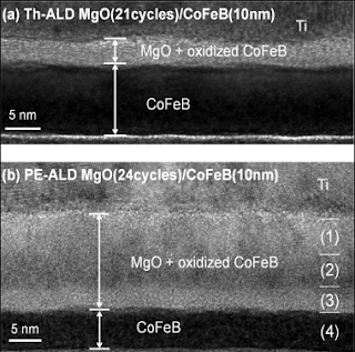
For example, Magnesium Oxide (MgO) is a semiconductor with a wide band-gap and semi-insulating properties. A very thin semi-insulating MgO layer between two metallic ferromagnetic layers is used as a “magnetic tunnel junction”. Magnetic tunneling junctions (MTJs) based on the CoFeB/MgO/CoFeB layer have received great attention as a promising candidate for future spin logic devices. Among various applications of MTJs, spin-transfer-torque magnetic random access memory (STT-MRAM) is emerging as a strong candidate as a next-generation nonvolatile memory due to its simple integration scheme, low voltage operation, and high speed. To fulfill certain critical requirements of 3D MTJ based sub-20 nm, high-density STT-MRAM, Samsung Advanced Institute of Technology (SAIT), Korea, has recently investigated both thermal and plasma-enhanced ALD for depositing a MgO tunnel barrier using bis(cyclopentadienyl)magnesium precursor under the scope of the Industrial Strategic Technology Development Program (10041926, Development of high-density plasma technologies for the thin-film deposition of nanoscale semiconductors and flexible-display processing) funded by the Ministry of Knowledge Economy (MKE, Korea). (Link)


Figure 1. TEM images of (a) Thermal ALD MgO, (b) PE-ALD MgO grown at 300 °C on a CoFeB layer

Recently, Panasonic Corporation, Japan, together with the National Institute of Material Science, Japan, reported ALD based Magnesium Phosphate (MgPO) thin-films as magnesium-ion conducting solid-state electrolytes that are considered to be promising candidates for future energy storage and conversion devices. The deposition was carried out at lower deposition temperatures, ranging from 125 to 300 °C, using bis(ethylcyclopentadienyl)magnesium. (Link)

Apart from semiconductor and energy storage applications, Mg is also an interesting candidate for astronomical and optical applications. For example, recent NASA missions that make observations in the ultraviolet, such as the Hubble Space Telescope and the Galaxy Evolution Explorer, employed primary mirrors coated with aluminum and further protected by thin films of Magnesium Fluoride (MgF2). Therefore, the Jet Propulsion Laboratory, California Institute of Technology, under a contract with NASA, reported ALD of MgF2 using bis(ethylcyclopentadienyl)magnesium supplied by Strem Chemicals, Inc. (Link)


Figure 2. Photograph of a concave mirror and convex diffraction grating for a next-generation UV instrument prototype coated with electron beam evaporated aluminum and a protective coating of 10 nm ALD MgF2 deposited at 150 °C.

Strem Chemicals, Inc., a leading fine chemicals supplier, headquartered in Newburyport, Massachusetts, USA, offers the most preferred precursors worldwide for ALD of Mg-based compounds, i.e, bis(ethylcyclopentadienyl)magnesium [Mg(CpEt)2] (catalog number 12-0510). The colorless to pale yellow liquid phase precursor with a density of 0.95 g/cm3 at 20 °C and vapor pressure of 0.0315 Torr is also sold by Strem Chemicals as pre-packed in cylinders:

§  98-4006: Bis(ethylcyclopentadienyl)magnesium, min. 98%, 12-0510, contained in 50 ml Swagelok® cylinder (96-1070) for CVD/ALD

§  98-4010: Bis(ethylcyclopentadienyl)magnesium, min. 98%, 12-0510, contained in high-temp 50 ml Swagelok® cylinder (96-1071) for CVD/ALD
 
About Strem Chemicals: Strem is an employee-owned fine chemicals supplier, manufacturing and marketing high-quality specialty chemicals for more than half-a-century. They provide custom synthesis and FDA inspected current good manufacturing practice (cGMP) services to its clients from academia as well as industry and also to government R&D labs. What distinguishes Strem from the other chemical suppliers are its ISO 9001 Quality Management System (QMS) standard and documenting procedures including for example “Color and Form” for every product as listed in the product details as a quality indicator for researchers. This helps Strem deliver precursors with a minimum metals purity of  99%, with some  some metal precursors attaining as high as 99.9999% metal’s purity. Strem offers over 5,000 specialty products in the area of metals, inorganics, organometallics, and nanomaterials. Strem’s product range includes:


Products Mentioned in this Blog:
12-0510: Bis(ethylcyclopentadienyl)magnesium, min. 98% (114460-02-5)
98-4006: Bis(ethylcyclopentadienyl)magnesium, min. 98%, 12-0510, contained in 50 ml Swagelok® cylinder (96-1070) for CVD/ALD
98-4010: Bis(ethylcyclopentadienyl)magnesium, min. 98%, 12-0510, contained in high-temp 50 ml Swagelok® cylinder (96-1071) for CVD/ALD


Related Product Lines & Resources:


----------
Promotional blog written and researched by Abhishekkumar Thakur and Jonas Sundqvist, BALD Engineering AB