Friday, April 10, 2020

AVS ALD/ALE2020 has been cancelled due to the Coronavirus pandemic

What a pain for us all, and especially for the organizers, because of the ongoing Coronavirus pandemic, it is unfortunate to report that the AVS-ALD2020 conference Gent, Belgium has been canceled.

AVS ALD/ALE 2020 web page and announcement: https://ald2020.avs.org/

According to information from the organizers, most likely, an online event will be organized with "virtual" plenary sessions and a possibility to upload a digital version of the presentation/poster. AVS is currently looking into this.

So 2020 turns out to be a challenging year for us all, if you want to get results or ALD products out there, please feel free to contribute to this blog. So if you have just published a paper, have a new ALD chamber on the market or a funky precursor - send it to me, and I will post it here ready for sharing in social media - it is for free!

Stay positive! Stay safe eveyrone! ALD - Let´s get it rolling!
Jonas 


Monday, April 6, 2020

White Paper: Atomic Layer Deposition for Quantum Devices

As the transistor gave rise to the information age, quantum technology has the potential to be the next great leap forward. Quantum technology is the application of quantum physics for real-world applications, such as quantum computing, sensing, navigation and communication.

Conventional methods for depositing superconductors include sputtering, pulsed laser deposition (PLD), and chemical vapour deposition (CVD). However, these methods can suffer from drawbacks including a lack of thickness control, poor uniformity and high impurity content.

Atomic layer deposition (ALD) is much more beneficial for thin-film deposition due to its ability to produce films with high purity, precise thickness control, conformal coating in high aspect ratio structures, and uniformity over large-area substrates.
 
 Download: LINK

Thursday, April 2, 2020

TSMC hit by 3nm delay fears over Covid-19 Lock-downs

TSMC is on schedule with its 5 nm process plan, but its 3 nm trial production may get delayed: The world's largest contract chipmaker is planning to launch mass production of its 3 nm process sometime in 2022, and media reported Monday that installation of production equipment in its 3 nm wafer fab in Tainan will be delayed to October from June this year, which will delay its trial production set for 2021. The COVID-19 escalation has hit Europe, and [Netherlands-based] ASML Holding, which is TSMC's major production equipment supplier, has been affected by a lockdown. It is understandable that the progress of TSMC's new technology has been affected.

Below a comparison of the Covid-19 daily new confirmed deaths, which is the only comparable parameter to use due to different testing capabilities and frequencies, in time and nation to nation. As can be seen the situation in Asian is under control after the gotten hit by the first wave of the Coronavirus. The European situation is stabilizing: Italy, Netherlands, Germany France, others look similar and are flattening the curve. In The USA situation is escalating. Many nations in Europe are forecasting a lift of Lockdown in May but are very careful, as an example Germany will decide in 19 April how to proceed according to Chancellor Dr. Angela Merkel.

BALD Engineering AB continues to monitor the Covid-19 situation due to lockdowns that affect the  the semiconductor industry – Stay Safe!

Google Finance (2020-04-02, 10:39 CET)

Sources:

Taiwan shares edge lower, TSMC hit by 3nm delay fears

Our World of data: https://ourworldindata.org/coronavirus

-----------
By Abhishekkumar Thakur, Jonas Sundqvist

Tuesday, March 31, 2020

Electronics Gas Market to reach $8.0B by 2024 despite expected COVID-19 impacts

San Diego, CA, March 30, 2019: TECHCET announced that the semiconductor fabrication gases market is forecasted as net positive in revenue growth for Q1, despite COVID-19. Although economic uncertainties for the remainder of the year may slow growth, current indications from the materials supply-chain look like "business as usual."

"Suppliers say that orders are strong," summarizes TECHCET President and CEO Lita Shon-Roy. "However, concerns exist that fabs may start to stock-pile materials to mitigate the possibility of interruption, especially from US suppliers that are now in the throes of the COVID-19 spread."

One recent positive for chip fabs is helium availability, where non-semiconductor demand is expected to ease. Given the COVID19 situation, medical and recreational (party balloons) helium demand will decline, allowing for the current shortage in the semiconductor supply-chain to mitigate sooner than expected. Major new sources like Gazprom, Arzew, and Qatar are scheduled to finally come online later this year.

TECHCET is also tracking potential disruptions in raw materials for critical gases—e.g. germanium for GeH4 and GeF4, fluorspar for HF, tungsten for WF6—has been minimal, because many Chinese suppliers had prepared safety stock for the Lunar New Year break.

Air Liquide, Air Products, Linde, Messer, and SK Materials have all announced increases in global production of gases. The market for both bulk- and specialty-gases is forecasted to grow from US$5.4B in 2019 to US$8.0B by 2024, as shown in the figure below. However, uncertainties exist for 2020 where demand may soften as a result of a prolonged impact of COVID19 on global economies.

TECHCET’s Critical Materials Report™ on Electronic Gases includes market landscape analysis and company profiles of Air Liquide, Linde, TNSC-Matheson, Versum Materials, Air Products, Showa Denko, SK Materials, Air Water, Hyosung, Peric, Kanto Denka Kogyo, and more. To purchase Report go to: https://techcet.com/product/gases/ 

Monday, March 30, 2020

Photonics for optical data transmission with Picosun’s Erbium ALD solutions

ESPOO, Finland, 30th March 2020 – Picosun Group reports excellent results in development of state-of-the-art photonics with its ALD (Atomic Layer Deposition) equipment and solutions.


Photonic devices such as waveguide amplifiers and lasers are central components in optical data transmission, a key technology realizing our modern, connected, information-driven society.

Silicon-integrated photonics take the technology one step further, enabling a whole new generation of microelectronics where optical solutions overcome some of the key challenges of conventional technologies.

Erbium-doped waveguide amplifiers and lasers are the most potential candidates for signal generation and amplification for telecommunication wavelengths. To reach the maximum performance of these devices, the amount and spatial distribution of dopant erbium atoms in the host material must be carefully optimized and controlled. This is where ALD shows its unique strength and beauty.

At Aalto University, Finland, Picosun’s customer Prof. Zhipei Sun’s group at the Finnish national infrastructure Micronova, and his international collaborators, have now used Picosun’s ALD technology to manufacture erbium-based silicon-integrated waveguide amplifiers with world-record performance(*).

“Silicon-integrated photonics, already employed by the leading companies in the field, are the future of microelectronics. We are very pleased of the performance of our PICOSUN® ALD equipment and the excellent quality of the Er:Al2O3 waveguide amplifiers manufactured with it. Customer support and consultancy from Picosun have always been there when we need it. ALD process is CMOS-compatible, further facilitating the integration of our waveguides into commercial chip production,” states Dr. John Rönn, the leading author of the results, from the Department of Electronics and Nanoengineering at Aalto University.

”ALD has been enabling disruptive future technologies since its invention. Picosun is happy to work with the leading experts in the field, such as our esteemed customers at the Aalto University. Our ALD solutions provide them the means to realize their groundbreaking work to develop yet more advanced communications and data transmission technologies for more connected, open, and integrated global society,” continues Mr. Edwin Wu, CEO of Picosun Asia Pte. Ltd

(*) The results were published in the journals ACS Photonics 3, 2040-2048 (2016) and Nature Communications 10, 432 (2019).

Covid-19 Update - European/US situation benchmarked with South Korea

Here is the latest plot that I make on the Covid-19 situation (Monday morning 2020-03-29 data) plotted as casualties per 1 million inhabitants for a number of countries in Europe + USA and benchmarking with South Korea. You can follow these and the dicussionon LinkedIn.

Soon there will be a podcast interview in Swedish English radio available on Spotify (LINK)


Saturday, March 28, 2020

Call for abstracts, ALD Applications ECS PRiME October 4-9, 2020 | Honolulu, Hawaii

PRiME 2020 Topic Close-up: Atomic Layer Deposition Applications 16
Symposium focus: This symposium contains cutting edge research results on applications in Atomic Layer Processing and will focus on a variety of applications of ALD and other atomic layer-by-layer processing (like etching and cleaning). 


The organizers would like to invite contributions to the following topics:
  • Semiconductor CMOS applications: development and integration of ALD high-k oxides and metal electrodes with conventional and high-mobility channel materials;
  • Volatile and non-volatile memory applications: extendibility, Flash, MIM, MIS, RF capacitors, etc.;
  • Interconnects and contacts: integration of ALD films with Cu and low-k materials;
  • Fundamentals of ALD processing: reaction mechanisms, in-situ measurement, modeling, theory;
  • New precursors and delivery systems;
  • Optical and photonic applications;
  • Coating of nanoporous materials by ALD;
  • MLD and hybrid ALD/MLD;
  • ALD for energy conversion applications such as fuel cells, photovoltaics, etc.;
  • ALD for energy storage applications;
  • Productivity enhancement, scale-up, and commercialization of ALD equipment and processes for rigid and flexible substrates, including roll-to-roll deposition;
  • Area-selective ALD;
  • Atomic Layer Etching (‘reverse ALD’) and related topics aiming at self-limited etching, such as atomic layer cleaning, etc.
Confirmed invited speakers:
  • Area-selective ALD processes for dielectrics, Sumit Agarwal, Colorado School of Mines, USA
  • Reactions on metal surface and diketone induced by gas cluster ions during Atomic Layer Etching, Noriaki Toyoda, Hyogo University, Japan
  • Molecular Layer Etching, Jeffrey Elam, Argonne National Laboratory, USA
  • Ga2O3 phase control and heterojunctions using PE-ALEpitaxy, Virginia Wheeler, US Naval Research Labs, USA
  • ALD for battery technologies, Arrelaine Dameron, Forge Nano, USA
  • ALD materials for solar fuels, Paul McIntyre, Stanford University, USA
  • Investigations into molecular layer deposition of conjugated amine polymers, Matthias Young, Univ. of Missouri, Columbia, USA
  • Functional Metal Oxides in Perovskite Solar Cells, Yu Duan, Jilin University, Changchun, China
  • In-situ and combinatorial techniques for spatial ALD, Kevin Musselman, University of Waterloo, Canada
  • Benefits of Spatial ALD compared to batch and single-wafer ALD methods, David Omeara, TEL Technology Center, America, USA
  • Surface thermolysis of ALD precursors and its implications for deposition, Xinwei Wang, Peking University, China
  • Recent developments in Materials characterization for the CMOS industry, Paul van der Heide, Imec, Belgium
  • MLD of metal-organic thin films with tuneable conductance for neuromorphic computing applications, Mikko Nisula, University of Ghent, Belgium
  • ALD of Phase Change and Threshold Switching Materials for Next-Generation Nonvolatile Memory Devices, Karl A. Littau, Intermolecular-EMD Group, USA
  • Coatings of (TiO2) Nanotube Layers, Jan Macak, University of Pardubice, Czech Republic
  • Recent development of various In-precursors and InOx related oxide semiconductor TFTs via ALD, Jin-Seong Park, Han Yang University, Korea

Deadline for submitting abstracts:
April 17, 2020

Thursday, March 26, 2020

NCD supplied two Lucida M300 ALD systems for R&D to KANC

NCD has recently supplied 2 Lucida M300PL ALD systems to KANC. Lucida M300PL-O is the equipment for oxide deposition with Ozone and Plasma process, and Lucida M300PL-M is that for metal deposition with Plasma process.

These wafer process equipment have the specification below

1) System: Lucida M300PL-O, Lucida M300PL-M

2) Substrate: Wafer 300mm

3) Deposition Materials:

- Lucida M300PL-O: Al2O3, TiO2, ZrO2, ZnO, HfO2, Ta2O5

- Lucida M300PL-M: Co. Ru, W, Ir, TiN, TaN

KANC, which is the most prestigious institute of Korea on nanotechnology, is using Lucida M300PL to investigate cutting edge semiconductor development and promising applications in MEMS and IoT. So it will be expected that these systems will contribute very much to the development of high-end nanotechnology.

NCD will do best to be the best ALD equipment company with continuous R&D efforts. 


< Lucida M300PL ALD >

Wednesday, March 25, 2020

ALD - Let´s get it rolling

First of all, an apology to all readers of the BALD Engineering ALD News Blog. There have been less than usual activities on the blog for the last couple of weeks. Recently I decided to quit my good safe job at Fraunhofer to start working as an ALD consultant and Blogger full time under BALD Engineering AB (LINK) and first and fore and most for TECHCET LLC CA (LINK). 

In February, I practiced my new life during our 2 week family winter holiday in Colombia and took some beautiful pictures from my different home offices on that fantastic trip.
 
Home Office at Playa Blanca, Isla Baru, Colombia
 
More recently, however, the Corona crisis hit us all, and I think everyone has gone through a time to adapt to a different type of life under these circumstances, and my romantic picture of the home office has changed a bit for now.

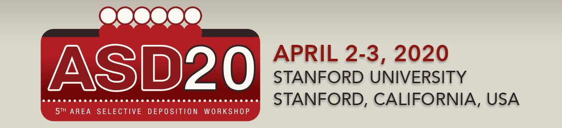
The first thing that hit me was postponing workshops and conferences, and I think many of you were looking forward to the ALD events in 2020. Here is a status overview of events I am either involved in or planned to join.

AVS ASD 2020 in Stanford, USA - will be moved (LINK)

EFDS ALD for Industry 2020 in Freiburg Germany - is moved to 2-3 December (LINK)

Novel High-k Workshop 2020 in Dresden, Germany - cancelled (LINK)
 
The Critical Materials Conference CMC2020 in Hillsboro, USA  - is moved to (LINK)

AVS ALD/ALE 2020 in Ghent Belgium - still scheduled to take place pending the situation (LINK)

Please let me know which 2020 events in addition to these that should be tracked here!

ALD - Let´s get it rolling

With this as a background, I decided that I need to get things moving again and that is why I now offer all of you who planned to participate in any of these or other ALD events 2020 to send me research news and /or promotional material fro your research or commercial products that you would like to get out there to the ALD community published here at this blog and shared in social media. 

Please send the material to me, and we will format it for the blog format and push it out to the ALD community - it is for free!

Two blogs (Strem and Beneq) are already in the pipeline, and I hope to see more from you - Stay Safe!

Contact: jonas.sundqvist@baldengineering.com


Typical back yard Hostel Home Office. Medellin, Colombia.

Hostel at the Caribbean, Always good coffee in Colombia!
 

Picosun reinforces local operations to ensure customer satisfaction during the COVID-19 epidemic

ESPOO, Finland, 23rd March 2020 – Picosun Group’s first priorities are customer satisfaction and health and wellbeing of the Group’s employees and customers. Picosun takes extremely seriously the global threat posed by the COVID-19 novel coronavirus epidemic and follows the rules set by governments and WHO. As the epidemic restricts global traveling, the importance of local offices and subsidiaries close to the customers is of utmost importance.


The last years have been the time of rapid growth and expansion for Picosun. Strong emphasis has been put on new recruitments especially on the service and support sector. Trained and qualified staff of service engineers are on call at the Group’s US locations in Texas, Arizona, and California and Asian locations in Japan, China, Taiwan, and Singapore. Dedicated sales and support personnel in Germany and France are available for the Group’s European customers. Local process support is also available on each continent.

At Picosun’s Finnish headquarters and local offices employees are encouraged to remote work from home whenever possible. Meetings are arranged virtually via video links and online platforms and inviting external visitors to the company’s premises is minimized to bare necessities. Cleaning of the premises and other hygiene measures have been intensified. All recruitment interviews are conducted remotely.

Despite of the challenging times, Picosun’s customer projects and deliveries continue. Process support and applications consultancy is always available from our Ph.D. level experts, and our Helpdesk serves 24/7 at support@picosun.com. Delivered PICOSUN® ALD system installations and commissioning, as well as customer support on-site, are taken care of by local Picosun offices with their trained and experienced staff.

“All of us here at Picosun wish good health and safety to everybody in this difficult and unexpected situation. In times like this, collaboration is the key to success and speedy recovery. Our business continues and we will put all our effort in sustaining the high level of quality that is the trademark of Picosun. We will further intensify our efforts to bring the benefits of ALD to medical industry. ALD is the very technology that enables our modern, mobile, data-driven and interconnected global society. Now is the time when this society can truly work together for better future,” says Jussi Rautee, CEO of the Picosun Group.

For more information regarding your projects or deliveries, please contact your respective Picosun sales or support contact person. For quotations for our ALD equipment and solutions, or process demo, please contact sales@picosun.com or coating@picosun.com, respectively.

As several expos and conferences the Group is sponsoring or exhibiting at have been postponed, please see the new dates in our event calendar on our website. Picosun is looking forward to meeting you all again later this year in good health and spirits!

Wednesday, March 4, 2020

Lam’s new Sense.i Etch platform delivers industry-leading output and innovative sensor technology

  • Lam Research (NASDAQ:LRCX) introduces the Sense.i tool, which etches finer 3D details on silicon wafers for chips.
  • The Sense.i platform enables the critical etch capabilities required to continue advancing uniformity and etch profile control for maximizing yield and lowering wafer costs
  • 3D features can help Lam customers like Samsung and SK Hynix put more memory capacity into small areas such as smartphones.
FREMONT, Calif., March 03, 2020 (LINK) -- Lam Research Corp. (Nasdaq: LRCX) today announced the launch of a completely transformed plasma etch technology and system solution, designed to provide chipmakers with advanced functionality and extendibility required for future innovation. Lam’s groundbreaking Sense.i™ platform offers unparalleled system intelligence in a compact, high-density architecture to deliver process performance at the highest productivity, supporting logic and memory device roadmaps through the coming decade.

youtube.com


With core technology evolved from Lam’s industry-leading Kiyo® and Flex® process modules, the Sense.i platform enables the critical etch capabilities required to continue advancing uniformity and etch profile control for maximizing yield and lowering wafer costs. As dimensions shrink and aspect ratios increase, the Sense.i platform is designed to support future technology inflections.

Powered by Lam’s Equipment Intelligence® technology, the self-aware Sense.i platform enables semiconductor manufacturers to capture and analyze data, identify patterns and trends, and specify actions for improvement. Sense.i also features autonomous calibration and maintenance capabilities that reduce downtime and labor costs, and delivers machine learning algorithms that allow the tool to self-adapt to minimize process variations and maximize wafer output.

The Sense.i platform has a revolutionary space-saving architecture that will help customers meet their future wafer output targets by producing more than a 50% improvement in etch output density. As semiconductor manufacturers develop smarter, faster, and denser chips, processes are rapidly growing in complexity and number of steps. This requires a greater number of process chambers in a fab and reduces total output for a given floor space. The Sense.i platform’s smaller footprint benefits either a new fab build or a fab undergoing a node-to-node technology conversion.

“Lam is introducing the most innovative etch product that has been developed in the last 20 years,” said Vahid Vahedi, senior vice president and general manager of the Etch product group at Lam Research (LRCX). “Sense.i extends our technology roadmap to meet our customers’ next-generation requirements while solving the critical cost scaling challenges they’re facing in their business. With more than four million wafers processed on Lam etch systems every month, Lam has an installed-base that provides extraordinary learning to innovate, design, and produce the best tools for semiconductor manufacturing.”

Thursday, February 27, 2020

Picosun delivers multiple production ALD systems to Asia for solid state lighting device manufacturing

ESPOO, Finland, 26th February 2020 (LINK) – Picosun Group, Finland-based, global provider of advanced Atomic Layer Deposition (ALD) thin film coating solutions, has been chosen by a major Asian customer to deliver significant ALD production capacity for manufacturing of solid state lighting devices. 

The PICOSUN® P-300BV ALD system is specially designed for production of LEDs, discrete devices, and MEMS devices such as print heads, sensors, and microphones.
 
Solid state illumination technologies are the future of lighting. Running on much lower power than other lighting devices and lasting much longer, they save both resources and environment. As small, compact and light-weight they are also simple to use in remote locations such as rural areas in developing countries, thus providing safe and easily powered lighting for example for children to study or health care stations to operate.

Picosun wants to introduce ALD to applications where it can improve both people’s quality of life and the state of the environment. Indeed, ALD is an ideal technology to enable various sustainable solutions, not only in lighting but in various other industries. In many cases, replacing thick, lower quality coatings with ultra-thin but superior quality ALD films leads to both material and energy savings and longer end product lifetime. Picosun’s equipment design, refined to top-notch performance through decades of cumulative experience in the field, ensures that no matter what industry, an optimal coating solution can always be found from the company’s portfolio.

“ALD films enhance the performance and lengthen the lifetime of solid state lighting devices. Our PICOSUN® P-300BV ALD system is specifically designed for these applications. It combines fast batch production capacity with vacuum loading for the highest ALD film quality and purity. We are happy to be chosen as the ALD technology provider for our esteemed customer. A facility of multiple P-300BV ALD tools that shall be installed in their premises will significantly strengthen our position in this market. For the end users, our ALD solutions enable flexible, power-saving and environmentally friendly lighting solutions with superb brightness and long life,” says Mr. Edwin Wu, CEO of Picosun Asia Pte. Ltd.

Tuesday, February 25, 2020

Schrödinger to give hands-on ALD simulation training in their ALD/ALE 2020 satellite workshop

AVS ALD is back in Europe this summer - Join Schrödinger scientists for hands-on ALD simulation training in their ALD/ALE 2020 satellite workshop taking place in Ghent on 2nd July 2020. Free, but spots are limited. Sign up at ow.ly/qHaz50ytPSC


Workshop:Simulating Atomic Layer Deposition and Etch
This day-long workshop will give hands-on training in the use of Schrödinger’s Materials Science Suite for the atomic-scale simulation of the chemistry of atomic layer deposition (ALD) and related gas-surface processes. Participants will get practical experience and in-person guidance in using the Maestro GUI, including the specialized model builders for molecules, organometallic precursors, bulk materials and surfaces. The quantum mechanics engines Jaguar and Quantum Espresso will be introduced. The workshop will also include a brief recap of background theory for quantum chemistry and some case studies of ALD simulations from the research literature.
Date & Time :Thursday, July 2nd ~ 09:00 - 16:00
Location:Ghent Marriott Hotel, Ghent, Belgium MAP
 

Monday, February 17, 2020

ALD Process For Preserving Lumber Could Offer Advantages Over Pressure Treating

[Georgia Institute of Technology News] Pressure treating – which involves putting lumber inside a pressurized watertight tank and forcing chemicals into the boards – has been used for more than a century to help stave off the fungus that causes wood rot in wet environments.


Now researchers at the Georgia Institute of Technology have developed a new method that could one day replace conventional pressure treating as a way to make lumber not only fungal-resistant but also nearly impervious to water – and more thermally insulating.

The new method, which was reported February 13 in the journal Langmuir (see below) and jointly sponsored by the Department of Defense, the Gulf Research Program, and the Westendorf Undergraduate Research Fund, involves applying a protective coating of metal oxide that is only a few atoms thick throughout the entire cellular structure of the wood.

This process, known as atomic layer deposition, is already frequently used in manufacturing microelectronics for computers and cell phones but now is being explored for new applications in commodity products such as wood. Like pressure treatments, the process is performed in an airtight chamber, but in this case the chamber is at low pressures to help the gas molecules permeate the entire wood structure.

Continue reading full article: LINK 
Publication: Shawn A. Gregory, Connor P. McGettigan, Emily K. McGuinness, David Misha Rodin, Shannon K. Yee, and Mark D. Losego, “Single-Cycle Atomic Layer Deposition (1cy-ALD) on Bulk Wood Lumber for Managing Moisture Content, Mold Growth, and Thermal Conductivity,” (Langmuir, February 2020). http://dx.doi.org/10.1021/acs.langmuir.9b03273


Wednesday, February 12, 2020

50th Hollow Cathode Gas Plasma Source Ordered from Meaglow Ltd

THUNDER BAY, Ontario--(BUSINESS WIRE)--In the semiconductor industry, hollow cathodes are best known for their application as sputter sources, however an increasingly successful range of gas plasma sources have been built by Meaglow Ltd for application in plasma enhanced atomic layer deposition (PE-ALD) and plasma enhanced chemical vapour deposition (PE-CVD). In the past, thin non-oxide films grown by PE-ALD had suffered from severe oxygen contamination problems, a problem that is largely solved with Meaglow’s hollow cathodes, which have the other advantages of high radical flux, low ion damage, and scalability. Meaglow has made several large area sources, in fact, the new order that pushes past the 50th plasma source is for three 4” diameter sources and an 8” diameter source for the OEM Okyay Tech (www.okyaytechald.com/) who will use the sources in some of their upcoming ALD equipment builds. Meaglow has also built 12” diameter sources for other customers.


“We believe Meaglow’s designs represent the first successful, wide spread, application of hollow cathode gas sources for thin film deposition,” says Dr. Scott Butcher, Chief Scientist of Meaglow Ltd. “Past designs struggled with uniform plasma distribution, a problem which Meaglow has overcome.” Dr Butcher’s early exposure to radiofrequency hollow cathode technology, back in the 1990s, was a good fit for solving some of the problems faced by our PE-ALD customers. Now our technology can be found in ten countries, and our customers have published over forty related journal papers, most of which are listed on our website.

About Meaglow Ltd.
Meaglow Ltd. Is a privately owned corporation in the industrial city of Thunder Bay, Canada. It’s range of next generation hollow cathode plasma sources is transforming the way plasma deposition is done. www.meaglow.com

Saturday, February 8, 2020

Consistency and reproducibility in atomic layer deposition

ALD is usually sold as a straight forward thin film deposition technique wit excellent film thickness university and straight forward thickness scaling by the number of ALD cycles applied. Here us a recently published paper in JVSTA from the leading ALD researchers at Argonne National Laboratory discussing the process result variation from processes used reported by the same precursor from equipment in different labs showing a rather significant variation. 

(As shared on LinkeIn, JVSTA Editors pick LINK)

Consistency and reproducibility in atomic layer deposition

Henrik H. Sønsteby, Angel Yanguas-Gil, and Jeffrey W. Elam
Journal of Vacuum Science & Technology A 38, 020804 (2020); https://doi.org/10.1116/1.5140603

Atomic layer deposition (ALD) is a thin film synthesis technique that can provide exquisite accuracy and precision in film thickness and composition even on complex, large area substrates. Based on self-limiting surface chemistry, ALD can be insensitive to process conditions and reactor designs, allowing an ALD process developed in one lab to be easily reproduced in other labs. In practice, however, ALD is sometimes difficult to reproduce or replicate, and the results can vary substantially between ALD reactors and between labs. This is exemplified by large deviations in reports on the growth of, e.g., Al2O3, FeOx, and TiO2 given the same precursors under similar conditions. Furthermore, the problem of irreproducibility seems to be growing as ALD is adopted by more researchers and integrated into new applications. In this article, the authors highlight some of the major sources of variations and errors and common misconceptions related to ALD. In particular, the authors focus on issues related to precursors, substrates, and deposition tools. The authors illustrate these problems through examples from the literature, and they present results from numerical simulations that describe how nonidealities would manifest in thickness profiles in a typical cross-flow reactor. They also describe how reproducibility in ALD is linked to consistent experimental practice and reporting between labs. The authors’ hope is that by educating newcomers to ALD and advocating for consistent reporting of deposition conditions, they can minimize irreproducibility and enable ALD practitioners to realize the full potential afforded by self-limiting surface chemistry

Friday, February 7, 2020

Veeco Introduces Suite of MOCVD Systems to Enable High Performance Photonics Devices

Plainview, N.Y. - Veeco Instruments Inc. (Nasdaq: VECO) introduced today the Lumina Metal Organic Chemical Vapor Deposition (MOCVD) platform, which incorporates the proprietary TurboDisc® reactor technology for outstanding film uniformity, yield and device performance for a variety of photonics applications. This new MOCVD platform, including the Lumina R480™ and Lumina R480S™ models, will accelerate the production of VCSEL, Edge-Emitting Laser (EEL) and Mini / Micro LED devices. 
 

(Image: Veeco)

In response to strong consumer demand for arsenic phosphide (As/P) MOCVD technology, the Lumina platform is advancing a new generation of high-efficiency photonics devices including VCSELs used in 3D sensing, autonomous driving and high-speed data communication. The Lumina platform is also designed for mini and micro LED production for advanced displays found in next-generation 4K and 8K televisions, smartphones and wearable devices, as well as EEL devices used for advanced optical communications and silicon photonics applications.

“Leading photonics manufacturers are currently seeing the benefits of our Lumina MOCVD system and are validating its impact in the manufacturing of high-volume photonics devices,” said Gerry Blumenstock, Senior Vice President, Product Line Management. “As the world’s leader in MOCVD equipment, the Lumina platform is the answer for the next generation VCSEL, EEL andmini / micro LED devices. With its proven design, technology and performance, Lumina provides exciting opportunities for the next generation of photonics devices.”

The Lumina R480 and R480S systems are based on Veeco’s industry leading MOCVD TurboDisc® technology which features excellent uniformity and low defectivity over long campaigns for exceptional yield and flexibility. In addition, Veeco’s proprietary technology drives uniform thermal control for excellent thickness and compositional uniformity. Providing a seamless wafer size transition, the system is capable of depositing high quality As/P epitaxial layers on wafers up to six inches in diameter. The R480 and R480S systems allow users to customize their systems for maximum value.

Veeco will be exhibiting at Photonics West in San Francisco, CA from Tuesday, February 4 to Thursday, February 6. Stop by booth number 1456 to learn more about Veeco’s MOCVD and ion beam sputtering solutions for photonics applications.

AVS ASD20 - Call for Abstracts MONDAY February 10, 2020

In an effort to help facilitate the progression of ASD techniques, the 5th Area Selective Deposition Workshop (ASD 2020) will act as a central event for sharing and discussing the newest developments in ASD by gathering leading experts from both academia and industry Attendees can expect to participate in talks regarding fundamental challenges related to recent developments in ASD, applications for ASD in next-generation technology, emergent processes for implementing ASD techniques, and new perspectives on metrological and characterization strategies for further understanding persistent mechanistic challenges. Based on the success of the previous workshops, ASD 2020 will consist of two days of presentations by invited and contributing speakers, as well as a banquet reception and poster session.


Abstract Deadline: February 10, 2020 LINK
 

Thursday, February 6, 2020

Forge Nano and ALD NanoSolutions to merge

Forge Nano and ALD NanoSolutions combine forces making atomic level manufacturing a reality

LOUISVILLE, CO., February 5th, 2020 —Leading atomic layer deposition (ALD) experts Forge Nano and ALD NanoSolutions merge to bring cutting edge surface engineering techniques to market.

The technology of tomorrow requires incredible precision and control of materials to make products perform better than ever before. By “starting at the surface” we can engineer exact material properties, at an atomic level. This allows us to optimize a number of characteristics by controlling the way surfaces behave and interact with one another and their environment.

By combining the cumulative experience and resources of our companies, we offer unmatched real-world expertise, and the ability to scale atomic surface technology all the way through to manufacturing. We enable the engineering and manufacturing of nano-coatings on particles, and high surface area objects using the precision of ALD.


“By consolidating and streamlining our organization we now have the resources to deliver on a whole new wave of atomically perfected materials. Our customers now have a one-stop shop for product development, manufacturing, and IP. I’m pleased to offer an even faster and more concise path to market for our partners.”

-Dr. Paul Lichty, CEO Forge Nano Inc.


“We are excited to merge our talent and resources to create a company with unmatched capabilities and technical know-how. Not only that, but we will continue our close collaboration with Prof. Alan Weimer, and Prof. Steven George and their research groups at CU Boulder, ushering in a new era of disruptive technology together.”

-Dr. Wayne Simmons, CEO ALD NanoSolutions Inc.


The future of advanced materials technology begins at the surface. Using finely tuned, sub-nano surface control, “Manufacturing with Atoms” becomes a reality that will create safer and more efficient products. ALD enabled surfaces are pushing past the limitations of today’s materials and are finding applications in not just industrial uses but also for many household products


Forge Nano is a global leader in surface engineering and precision nano-coating technology. Our proprietary technology and manufacturing processes make angstrom-thick coatings fast, affordable and commercially viable for a wide range of materials, applications and industries. Our suite of ALD products and services covers the full spectrum from lab-scale to pilot and commercial-scale manufacturing systems. www.ForgeNano.com

Tuesday, February 4, 2020

Swagelok ALD20 UHP Valve Offers New Possibilities for Semiconductor Production

Advanced valve enables chip fabricators to experiment with new precursors due to higher flow capacity, thermal stability, and extreme precision.


SOLON, Ohio--(BUSINESS WIRE)--#ALD--Swagelok, a leading solutions provider of fluid system products, assemblies, and related services, has announced the release of a new ultrahigh-purity (UHP) valve for high-flow applications—the ALD20. Since introducing atomic layer deposition (ALD) valve technology to the market, Swagelok has worked with semiconductor tool manufacturers and chip fabricators to provide the performance needed to keep pace with quickly changing process requirements. The new ALD20 valve is the latest result of this collaboration, allowing forward-thinking process designers the flexibility to experiment with low-vapor pressure chemistries that may hold the key to tomorrow’s competitive advantage.

The ALD20’s patent-pending design maximizes production process efficiency and deposition consistency by providing flow coefficients two to three times what can be achieved using today’s standard ALD valve technology. It can deliver a flow rate of up to 1.2 Cv in the same footprint (1.5 in.) as existing ALD valves, allowing some users to boost throughput without retooling existing equipment or making additional process changes. The other standard version ALD20 valve with a slightly larger footprint width (1.75 in.) provides an even greater flow rate of up to 1.7 Cv. Custom set flow coefficients are also available.

Swagelok ALD20 UHP Valve(Swagelok.com)
 
Designed for peak process consistency, the ALD20 can be fully immersible in a gas box from 50°F (10°C) up to 392°F (200°C), enhancing thermal stability and deposition uniformity. It also features a valve body comprised of 316L VIM-VAR stainless steel or Alloy 22—offering enhanced corrosion resistance to withstand aggressive media—as well as a highly polished bellows with a 5 μin. Ra finish to support clean operation for long-term process integrity.

“The ALD20 is a direct response to the rapidly evolving needs of the semiconductor industry,” said Garrick Joseph, director of marketing, semiconductor, for Swagelok. “Through partnership with industry leaders and application of fluid system engineering expertise, we are pleased to launch a product that allows customers to effectively use precursor gas chemistries that previously may have been considered too challenging or too expensive to employ, but which could be crucial to the development of the next generation of chip technology.”

The ALD20 is available today in modular surface-mount configurations with two or three ports, in straight configurations with tube butt weld and male or female VCR® face seal fitting end connections, and in multiport valve configurations to optimize flow paths within existing or new systems. A high-temperature optical position sensor is available as an add-on component as well.


Thursday, January 30, 2020

Picosun’s ALD technology helps to fight climate change

ESPOO, Finland, 30th January 2020 – Picosun’s Atomic Layer Deposition (ALD) thin film barrier coating technology offers a solution for eliminating the use of hazardous process gases, sulphur hexafluoride (SF6) and nitrogen trifluoride (NF3).

In the current Chemical Vapor Deposition (CVD) coating methods, relatively thick films need to be grown to obtain the desired level of performance to reach the required specifications in e.g. moisture barrier, corrosion protection, passivation or insulation applications. Due to the fast film build-up on the walls of the coating equipment, the deposition chamber has to be cleaned of film residues at regular intervals. This is typically done by a chamber cleaning process with SF6 or NF3 plasma.


SF6 is the strongest greenhouse gas ever known, with global warming potential of 22600 times that of CO2 (for NF3, the coefficient is 17200) and it stays in the atmosphere for at least 1000 years (*). SF6 emissions in the EU in 2017 alone had greenhouse gas effect equalling that of 1,4 million cars (**). Hence, usage of these gases is subject to constant scrutiny and increased regulation.

By switching to Picosun’s ALD nanolaminate barrier technology it is possible to obtain unmatched barrier performance with extremely thin, pinhole-free films. This also eliminates the need to clean the deposition equipment after every few process runs. In typical production use, Picosun’s ALD reaction chamber is cleaned only once per 3 – 6 months, and simple mechanical bead blasting instead of fluorine-based plasma treatment is enough.

“We at Picosun want to employ our ALD technology for sustainable future. Fighting the climate change by all possible means requires collaboration between the innovative industries and solution providers. By replacing thick coatings, manufactured with environmentally compromising, energy- and resource-intensive methods, with our ultra-thin ALD film stacks, significant material and cost savings are obtained and hazardous gases are not needed in equipment cleaning,” summarizes Mr. Juhana Kostamo, deputy CEO of Picosun Group.

Picosun provides the most advanced AGILE ALD® (Atomic Layer Deposition) thin film coating solutions for global industries. Picosun’s ALD solutions enable technological leap into the future, with turn-key production processes and unmatched, pioneering expertise in the field – dating back to the invention of the technology itself. Today, PICOSUN® ALD equipment are in daily manufacturing use in numerous leading industries around the world. Picosun is based in Finland, with subsidiaries in Germany, North America, Singapore, Taiwan, China and Japan, offices in India and France, and a world-wide sales and support network. Visit www.picosun.com.

(*) J-C. Cigal et.al.: “On-site fluorine chamber cleaning for semiconductor thin-film processes: Shorter cycle times, lower greenhouse gas emissions, and lower power requirements”, DOI: 10.1109/ASMC.2016.7491126

(**) P. Widger et.al.: “Evaluation of SF6 leakage from gas insulated equipment on electricity networks in Great Britain”, DOI: 10.3390/en11082037