Wednesday, September 25, 2019

Device Engineer at Petabyte in Shanghai for FRAM Cell/Array engineering


Job Description

This position is for a Device/Testing Engineer working on FRAM Cell/Array engineering. The engineer is responsible for leading research and development of next generation VFRAM to support Petabyte Technology Inc’s (PBT) growing business in storage and memory solutions. Primary responsibilities include silicon experimentation, cell and array characterization, data analysis, modelling of the device, array, circuits and system behavior to meet complete product requirements and system needs. The engineer is also responsible for developing innovative device solutions and memory operation algorithms to continue technology scaling. Successful candidate will collaborate with process integration engineers, circuit designers, product engineers to understand the critical issues and inter-dependencies and engineer solutions to address them.

Location: Shanghai, China
Traveling: <20%
Salary: TBD
Language: English/Chinese

Qualifications

Education:Candidate should possess an MS degree with at least 4 years additional experience, or a PhD with at least 2 years additional experience, in Electrical Engineering or Physics, with an emphasis in Physics of Semiconductor Materials or Devices/Testing related areas.

Hands on experience with FRAM/FEFET in device and testing are strongly preferred!!

Bench testing experience is preferred but not required.

Device modeling is preferred but no required.

Minimum Requirements:
- 4+ years' experience in the area of Semiconductor and Device Physics, or device processing, electrical characterization, and device and circuit models.
- 4+ years' experience in technical problem solving.

About PBT

Petabyte Technologies is a high-tech enterprise focusing on the R&D and sales of new memory chip - FRAM, a new kind of NVM(Non-Volatile Memory). The project team brings together the world's top experts in memory development, with an average of more than 15 years of cutting-edge technology experience.

The FRAM technology, Petabyte’s proprietary intellectual property, adopts brand new material and architecture. The FRAM memory is designed to fill the gap between the two main stream memories, DRAM and Flash. It is equipped with fast read-write speed, accurate addressing to byte, high durability, flash-like non-volatility and low power consumption. Petabyte’s FRAM can immensely increase storage density current memories.

FRAM has a wide application such as future smart market (including household, office, instrumentation, automotive electronics) and AI chips market.

About Our Group

The Cell development Group is responsible for delivering new memory Cell solutions to PBT’s (Petabyte Technology. Inc) most advanced memory products. As part of the cell development team, we develop the best-in-class materials solutions and partner with process integration, product and Design teams to introduce these solutions into new memory products. As an enabler of head performance and reliability advances through cell innovation, we help PBT lead in technology and time-to-market.

Contact:

Sharon Yin

E-mail: xryin@petabytetech.com

Mobile:(+86)18914135998

Wechat:13921177520


Beneq unveils Transform(TM), a versatile automated ALD platform for More-than-Moore device fabrication

Combination of thermal and plasma ALD, single wafer or batch processing, and a unique preheating module maximize options for flexible volume production

25 September, 2019, Grenoble, France – Beneq, a leading provider of ALD R&D and production technology, today announced the BENEQ TransformTM, a versatile ALD platform dedicated to More-than-Moore device fabrication.


The brand-new cluster design offers customers unparalleled flexibility by combining both thermal and plasma ALD with single wafer and batch processing, on a single automated platform. Fully compliant with industry quality and SEMI standards the BENEQ TransformTM is a one-stop ALD solution for Power Electronics, MEMS and Sensors, RF, LED, Photonics, and Advanced Packaging applications.

“Among hundreds of application requests brought to us by customers today, we are most excited by GaN devices for RF and Power applications as well as Photonics, both III-V and Silicon,” said Dr. Patrick Rabinzohn, Beneq’s Semiconductor Business Executive. “In particular surface passivation, gate dielectrics, nucleation layers and encapsulation layers are all well addressed with the BENEQ TransformTM.”

Truly Versatile


More than Moore (MtM) applications are evolving at a phenomenal pace. To be competitive manufacturers are adopting advanced thin film technologies. Often, they need to combine surface preparation, interfacial layer and functional layer deposition sequences - all in one tool.

Currently available ALD production systems offer only one type of ALD process - either thermal or plasma enhanced. This creates the need for a versatile tool that supports multiple deposition capabilities.

The BENEQ TransformTM confidently combines thermal and plasma ALD processing, on a single wafer or in batches, while easily configurable. It is capable of surface pre-treatment and can coat substrate materials at wafer sizes from 3 to 8 inches.

It works well for R&D, prototyping, as well as volume production. With the BENEQ TransformTM customers now have the option to run several different ALD processes on multiple devices and applications, all on a single footprint!

The most complete configuration offers two ALD process modules, pre-heating station, surface plasma treatment and wafer cooling.

Designed for the Fab


Unlike ALD production platforms featuring vertical flip functions, the TransformTM loads wafers in a horizontal position and seamlessly integrates with the rest of your production line. Such a loading mechanism is also proven to minimize handling issues, and particle generation associated with non-standard cassette batch loading systems.

The BENEQ TransformTM features a proprietary preheating module that eliminates hours of waiting time and boosts throughput to a whole new level (15 wph @50 nm Al2O3, in thermal mode). Throughput can be further increased by adding up to 2 more process modules, thermal or plasma.

The BENEQ TransformTM produces a wide range of oxides including Al2O3, HfO2, Ta2O5, TiO2, and SiO2, and nitrides such as AIN and TiN. What sets the TransformTM apart from other tools is its ability to scale up throughput and maintain the same uniformity regardless of the temperature, e.g. >400°C.

SEMI Certified


The BENEQ TransformTM shortens cycle time and speeds up fab adaptation by implementing SECS/GEM standards. It is fully compliant with SEMI S2/S8 for environmental, ergonomics and safe operations.

To learn more, visit www.beneq.com/transform.

About Beneq

Beneq is the home of ALD, offering a wide portfolio of equipment products and development services. Today Beneq leads the market with innovative solutions for flexible high-volume manufacturing (BENEQ TransformTM), advanced R&D (TFS 200, R2), ultra-fast high precision spatial ALD coatings (C2R), roll-to-roll thin film coating of continuous webs (WCS 600), and specialized batch production for thicker film stacks (P400, P800). Headquartered in Espoo, Finland Beneq is dedicated to making ALD technology accessible for researchers and providing the invisible advantage in emerging semiconductor applications.

Press Contact
Lie Luo
Beneq
lie.luo@beneq.com


Tuesday, September 24, 2019

Moore's Law graphed vs real CPUs & GPUs 1965 - 2019


(Youtube: https://www.youtube.com/watch?v=7uvUiq_jTLM) Moore's Law has been ridiculously accurate for more than 50 years - how long will it hold up? See in this visualization how the actual transistors in CPUs and GPUs compare to the linear progression of Moore's Law. From the early days of microprocessors, to Intel dominance and the rise of GPUs. 
 
Music: Dizaro - Aurora Borealis https://theartistunion.com/dizarofr 
Data sources: Too many to list here, see wikipedia article: https://en.wikipedia.org/w/index.php?... for Moore's Law, I took a starting point of 8000 in 1975, and worked my way forward and backward from there.

Monday, September 23, 2019

Intel at EECS Colloquium "Moore’s Law Is Not Dead"

Intel’s Jim Keller: “We’re all building nanowires… Intel, TSMC, Samsung” Keller in his "Moore’s Law Is Not Dead" talk at UC Berkeley this week said, “We had planar transistors, we went to FinFET. We’re all building nanowires in the fab. Intel, TSMC, Samsung, everybody’s working on it. There’s a really interesting thing. While the world thinks Moore’s Law’s dead, the fabs and the technologists think it’s not and everybody’s announced now a 10-year roadmap for Moore’s Law.” 


The UC Berkeley EECS Events team has live streamed the entire talk over on YouTube and you can catch up on this fascinating, intimate little talk (below).
 
 ----------
By Abhishekkumar Thakur

Sunday, September 22, 2019

Strategy Utilizing Electrochemical ALD of Cu-Zn for Enabling Metallization of Sub-10 nm Semiconductor Device Nodes


Strategy Utilizing Electrochemical ALD of Cu-Zn for Enabling Metallization of Sub-10 nm Semiconductor Device Nodes

Aniruddha Joi, Kailash Venkatraman, Kuang-Chih Tso, Dries Dictus, Yezdi Dordi, Pu-Wei Wu, Chih-Wen Pao and Rohan Akolkar

doi: 10.1149/2.0181909 jss ECS J. Solid State Sci. Technol. volume 8, issue 9, P516-P521 

A novel interface engineering approach, utilizing electrochemical atomic layer deposition (e-ALD) of Cu(Zn) on a Ru liner, is presented for enabling the metallization of sub-10 nm interconnects in future semiconductor devices. Upon thermal treatment, Zn present in the e-ALD Cu layer at ∼0.8 at.% is shown to diffuse through the Ru liner and react with the SiO2 to form a Zn-silicate layer at the Ru-SiO2 interface. This ‘self-forming’ interfacial layer provides adhesion enhancement to the Ru-SiO2 interface and serves as a diffusion barrier retarding Cu diffusion into the SiO2 layer while enabling void-free gap-filling of high aspect ratio trench structures. Absorption Near-Edge Spectroscopy and Extended X-ray Absorption Fine Structure analyses confirm that the self-formed barrier layer is composed primarily of Zn2SiO4. The interface engineering approach utilizing Cu(Zn) presented herein offers several potential advantages over traditional Mn-based self-forming barrier approaches, i.e., scalability to narrower dimensions and minimal impact to interconnect resistance.


Process flow for adhesion testing by scratch and peel method for (a) Cu/Cu-Zn/Ru/SiO2 and (b) Cu/Ru/SiO2 stack without the Zn-containing interlayer.

Picosun Regional Sales and Service Manager, Europe – Dresden, Germany

Picosun is now searching for a Regional Sales and Service Manager for sales and customer support in Central Europe, mainly in German speaking countries. You will be located at the Picosun office in Dresden, Germany, and you will be working closely with customers and Picosun’s European sales, application and service teams.

Main Duties

  • Customer support in Central Europe
    ­
  • Managing existing customers and building new customer base together with Picosun sales, application and service teams and service subcontractors
    ­
  • Developing and maintaining lasting relationships with the customers and other partners
    ­
  • Providing responses to customers’ technical enquiries
    ­
  • Participating in hands-on selling, in support including repair and servicing the equipment, and in training of the customers

Desired Skills and Experience

  • Degree in engineering (e.g. in Electronics, Chemistry or Physics) is preferred
    ­
  • Experience in customer service with a strong focus on customer satisfaction
    ­
  • Experience in semiconductor processes and equipment
    ­
  • Field service and maintenance experience
    ­
  • Problem solving
    ­
  • Willingness to travel
    ­
  • Good communications and interpersonal skills
    ­
  • Hands on experience in automation and vacuum systems is a plus
Please send your application and CV to hr@picosun.com. For heading/subject please write “Sales and Service Manager – Germany”.

For additional information, you may contact Christoph Hossbach, christoph.hossbach@picosun.com, +49 1522 44 949 11, General Manager of Picosun Europe GmbH.

Thursday, September 12, 2019

The website for the 2020 Area Selective Deposition Workshop is now live!

Developments in nanoelectronics and nanoscale surface modification have continued to drive the need for more elegant and reliable bottom-up area selective deposition (ASD) strategies. Most notably, the semiconductor industry has relentlessly pursued sub-10 nm transistor fabrication for next-generation devices, an endeavor that increasingly relies on selective deposition techniques to facilitate proper material alignment. However, other fields beyond traditional transistor fabrication have also found potential applications for selective deposition. Mixed-material catalysts have consistently shown the benefits of having site-specific material growth, but new optical devices and materials for energy storage have also contributed to an increased focus on developing new strategies for ASD.


In an effort to help facilitate the progression of ASD techniques, Stanford University is proud to host the 5th Area Selective Deposition Workshop (ASD 2020), held on April 2–3, 2020 in Palo Alto, California USA. Located in the heart of Silicon Valley, this year’s workshop will act as a central event for sharing and discussing the newest developments in ASD by gathering leading experts from both academia and industry. Attendees can expect to participate in talks regarding fundamental challenges related to recent developments in ASD, applications for ASD in next-generation technology, emergent processes for implementing ASD techniques, and new perspectives on metrological and characterization strategies for further understanding persistent mechanistic challenges.

Based on the success of the previous workshops, ASD 2020 will consist of two days of presentations by invited and contributing speakers, as well as a banquet reception and poster session at Stanford University. We hope that guests will also have time to experience some of the local attractions and natural beauty that the Bay Area has to offer!

Wednesday, September 11, 2019

Industrial Atomic Layer Deposition for Image Sensors and Light Sources

Here is an interview by SEMI (LINK) with Dr. Mikko Söderlund, sales director for Beneq’s semiconductor business. The interview is about trends in ALD applications. Söderlund shared his views ahead of his presentation at SEMI MEMS & Imaging Sensors Summit, 25-27 September, 2019, at the WTC in Grenoble, France. Besides the leading edge 300 mm semi market Beneq sees ALD growth in the following markets.

  • Backside Illuminated (BSI) CMOS Image Sensors (CIS)  
  • MEMS (actuators and sensors, RF) 
  • GaN Power and RF
  • Photonics.


Dr. Mikko Söderlund is the Sales Director for Beneq’s semiconductor business. He has more than 20 years of experience in product development, product management, technical sales and business development across Photonics, OLED, and Semiconductor industries. Mikko received his Ph.D. in Micro- and Nanotechnology from the Helsinki University of Technology.
 

Tuesday, September 10, 2019

LG Technology Ventures & Mitsui Kinzoku-SBI Material Innovation Fund Join Forge Nano Inc. Series A

LOUISVILLE, Colo., Sept. 5, 2019 /PRNewswire/ -- Mitsui Kinzoku-SBI Material Innovation Fund and LG Technology Ventures join in Forge Nano's Series A, bringing the total investment to date to $18M, up from Volkswagen's initial $10M investment announced in January 2019.

The investment will help to accelerate advanced materials for new battery technologies while also broadening applications for atomic-level nano-coatings into a diverse set of new markets. Forge Nano's technology paves the way for entirely new applications for nanoscale surface engineering. Atomic layer deposition (ALD) is an ultra-thin film deposition process that allows precision coatings that are the thickness of one atom to be deposited one layer at a time onto a surface. Forge Nano's ALD enabled core-shell battery materials have been demonstrated to improve the energy density, charge rate, cycle life, and safety of lithium-ion batteries as well as to enable next generation battery technologies.

Beyond batteries, ALD nano-coatings are enabling the next era of higher performance materials for catalysts, 3D printing, thermal fillers, separations and an array of other new market applications. Virtually any application using industrial powders that benefit from tuned surface properties but require precise, uniform and conformal coatings that are chemically bonded to the surface can now use ALD nano-coatings to unlock the next level of performance and value.

"Forge's proprietary nano-coating technology and high-throughput manufacturing processes will open the door for a new stage of high performance materials. A collaboration between Forge Nano and Mitsui Kinzoku will accelerate the production of high performance materials and provide our customers high value products in various market."
-Mitsui Kinzoku-SBI Material Innovation Fund

About Mitsui Kinzoku-SBI Material Innovation Fund: Mitsui Kinzoku-SBI Material Innovation Fund was jointly established in 2017 by Mitsui Kinzoku and SBI Investment. Its investment target is start-up companies with material technologies, material manufacturing and processing know-how which are each likely to generate a business synergy effect with Mitsui Kinzoku's business.

About LG Technology Ventures: LG Technology Ventures was established in 2018 and is the venture capital investment arm of the LG Group of South Korea. The LG Technology Ventures team consists of experienced investors, entrepreneurs, technologists, and industry domain experts. Currently, LG Technology Ventures is managing over $400 million of fund assets and invests in early-stage information technology, automotive, manufacturing, life-sciences, energy, and advanced materials companies.

About Forge Nano: Based in Louisville, Colo., Forge Nano is a global leader in surface engineering and precision nano-coating technology. Forge Nano's proprietary technology and manufacturing processes make angstrom-thick coatings fast, affordable and commercially viable for a wide range of materials, applications and industries. Forge Nano's suite of ALD products and services covers the full spectrum from lab-scale to pilot and commercial-scale manufacturing systems. For more information visit www.ForgeNano.com

Monday, September 9, 2019

ALD PhD Thesises form the dawn of time

Number of PhD thesis' about Atomic Layer Deposition (ALD), according to data collector in the VPHA, up to sept. 2019

Presentations of the EuroCVD 22 – Baltic ALD 16 | 2019 conference for download

Please find below the presentations of the EuroCVD 22 – Baltic ALD 16 | 2019 conference (Luxembourg - June 24 to 28, 2019) that has been published online so far (LINK)


Programme: LINK

Invited speakers:
Oral presentations:

Abstracts

Abstracts_Oral_Presentations_Day_1
Abstracts_Oral_Presentations_Day_2
Abstracts_Oral_Presentations_Day_3
Abstracts_Oral_Presentations_Day_4
Abstracts_Oral_Presentations_Day_5

Friday, September 6, 2019

Hydrogen diffusion barrier using thermal ALD Al2O3 encapsulation for IGZO TFTs

Amorphous phase In-Ga-Zn-O(IGZO), the typical oxide TFT compositions, has 20 to 50 times higher of field-effect mobility than that of a-Si TFTs and excellent SS (Sub-Threshold Voltage Swing) properties as well as has been very promising to apply for high performance and large area displays and for transparent displays due to their superior properties and good uniformity.

But IGZO TFTs with PECVD SiNx as an encapsulation layer have degraded their superb properties because hydrogen included in SiNx from 20% to 30% has passed through OLED layers and then diffused into IGZO layers.


Comparison of I-V characteristic of a-IGZO TFTs with and without hydrogen diffusio


If this performance degradation by hydrogen diffusion showed in typical I-V graph, SS slop would be decreased, Ioff increased and Vth shifted to negative direction from the original I-V curve.

In case of applying to OLED display with IGZO TFTs using SiNx encapsulation layers including hydrogen, Al2O3 layers would be the very excellent barriers not to degrade IGZO TFTs properties by diffusion of hydrogen from SiNx.

However it is not good choice to apply PEALD Al2O3 using plasma to the first encapsulation layer because oxygen plasma could cause the side effect such as cathode oxidation during the process. So IGZO TFTs and thermal ALD Al2O3 encapsulation layers without plasma damage could be optimum combination.

NCD Lucida GD Series that is thermal ALD batch equipment for mass production to deposit on large substrates up to 6th generation glasses could provide superior Al2O3 hydrogen barriers preventing diffusion into IGZO TFTs from PECVD SiNx encapsulation layers including hydrogen as well as expect to apply to transparent fordable OLED displays by using Al2O3/Polymer/Al2O3 encapsulation layers.


NCD’s LucidaTM GD Series ALD

Tuesday, September 3, 2019

ALD - Why ASMI is doing so well

[BITS&CHIPS] Grueling work with Intel cemented the company’s position in the atomic layer deposition market, but the emergence of more ALD semiconductor applications was required for that investment to really pay off. The story of why ASM International is doing so well these days.

ASM International is on a roll. While the semiconductor industry has been experiencing a cold spell since mid to late 2018, the Almere-based semiconductor equipment maker has been posting one quarterly sales growth after the other. Last July, front-end sales even reached an all-time record – and the orders keep pouring in. Many of those are for ASMI’s atomic layer deposition (ALD) systems, which at the moment are its best selling product line, CEO Chuck del Prado noted in a conference call with investors, though he added demand is generally healthy in other businesses as well.
Full story: When persistence pays off: why ASMI is doing so well [LINK]
An ASM Pulsar 2000 form the year 2000 (Photo CAE LINK), which was used by many semiconductor fabs for the early development of ALD High-k in both logic and DRAM (Al2O3, ZrO2, HfO2, and others). One of the first high volume manufacturing applications was dielectric layers for GMR and TMR magnetic heads by, e.g., Seagate. The 200 mm single wafer ALD reactor was later made as a 300 mm reactor for the first roll-out of high-k ALD at Intel 45 nm node in 2007. The Pulsar was typical at the beginning used on the Polygon platform. However, now it is available on the new more productive XP series of the ASM platforms (LINK).

Thursday, August 29, 2019

Picosun launch new high power Micro Wave Plasma ALD

ESPOO, Finland, 29th August 2019 – Picosun Group, the leading supplier of AGILE ALD® (Atomic Layer Deposition) thin film coating solutions, reports excellent results obtained with its next generation R&D PEALD (plasma-enhanced ALD) technology.

PEALD enables deposition at low temperatures and of several materials that could not be deposited with thermal process only. The drawback of PEALD, however, is damage to the sample surface, caused by ion bombardment. Picosun’s solution to this is remote plasma method, where the plasma source is located high enough above the sample, and the reactive species hitting the surface are radicals, not high-energy ions.

“Picosun’s operating philosophy is based on constant improvement and development, as we want to offer our customers always the best-in-class, leading quality ALD solutions. Our Picoplasma™ equipment has been a hit product in the R&D community since its launch, and we have now upgraded it to a completely new level, to enable even faster processing with superior film quality and purity,” says Dr. Jani Kivioja, CTO of Picosun Group.

Picosun’s next generation PEALD solution is based on remote, high power microwave plasma (MWP). The compact, lightweight plasma generator can be integrated to existing PICOSUN® R&D ALD reactors as such. The new plasma-ALD solution realizes deposition with virtually no added particles, with extremely low metal contamination and with far shorter cycle times compared to the previously used method. Excellent film quality and uniformity have been obtained(*), and the new MWP allows wider operating range (in terms of plasma parameters) which widens also the selection of available ALD processes.

“We are pleased to provide our customers with our new, thoroughly upgraded plasma-ALD solution. There are several important application areas, such as medical devices and MEMS, where substrates are sensitive and require processing at low temperatures. Now we have an ideal solution to this, which will again facilitate ALD’s breakthrough to yet new components and devices,” continues Dr. Kivioja.

(*) Film properties, SiO2 as an example:
 
Wafer size Dep. temperature GPC Film non-uniformity (1σ, 5mm EE, 49pts) Leakage current (@4MV) Particles (@>0,25µm) Metal contamination (Fe, Ti, Cr, Mn, Ni, Cu, Zn atoms)
200 mm 400 °C 0.86 Å/cycle 1.7 % (~10 nm film) 2.1 x 10⁻⁸ A/cm2 < 60 < 2 x 10¹⁰ /cm2
 

Tuesday, August 27, 2019

New coating paves the way for low weight lithium metal batteries

A Dynamic, Electrolyte-Blocking, and Single-Ion-Conductive Network for Stable Lithium-Metal Anodes

Zhiao Yu, David G. Mackanic, Wesley Michaels, Jian Qin, Yi Cui, Zhenan Bao
Published:August 26, 2019 DOI:https://doi.org/10.1016/j.joule.2019.07.025

Highlights

  • A multifunctional network material is proposed to stabilize lithium-metal anodes
  • Improved cyclability is achieved for high-voltage lithium-metal full battery
  • Direct lithium-metal processability enables practical application
  • Crosslinking chemistry is tuned to study the synergistic stabilizing effects

Implementation of lithium (Li)-metal anodes requires developments to solve the heterogeneity and instability issues of naturally formed solid-electrolyte interphase (SEI). The artificial SEI, as an alternative, enables an ideal interface by regulating critical features such as fast ion transport, conformal protection, and parasitic reaction mitigation. Herein, for the first time, we integrate all of these desired properties into a single matrix, the dynamic single-ion-conductive network (DSN), as a multifunctional artificial SEI. The DSN incorporates the tetrahedral Al(OR) 4 − (R = soft fluorinated linker) centers as both dynamic bonding motifs and counter anions, endowing it with flowability and Li + single-ion conductivity. Simultaneously, the fluorinated linkers provide chain mobility and electrolyte-blocking capability. A solution-processed DSN coating was found to simultaneously hinder electrolyte penetration, mitigate side reactions between Li and electrolyte, maintain low interfacial impedance, and allow homogenous Li deposition. With this coating, long cycle life and high Coulombic efficiency are achieved for Li-metal battery in a commercial carbonate electrolyte.


Surface-Inhibiting Effect in Chemical Vapor Deposition of Boron–Carbon Thin Films from Trimethylboron

Here are deep insights to the understand of conformal boron-carbon films in very high aspect ratio structures by researchers from Linköping University, Sweden. If you don't have the journal access, please check the pre-print (LINK).

Surface-Inhibiting Effect in Chemical Vapor Deposition of Boron–Carbon Thin Films from Trimethylboron

Laurent Souqui, Hans Högberg, Henrik Pedersen
Chem. Mater. 201931155408-5412 LINK


We use the ability to control surface chemistry in chemical vapor deposition (CVD) to deposit boron–carbon films into pores with an aspect ratio of 60:1 without clogging the opening, and into lateral trenches with ratios of up to 2000:1. In contrast to many other surface-controlled CVD processes, operating at low temperatures (100–250 °C) and pressures (10–1000 Pa), we use trimethylboron at a higher temperature (700 °C) and pressure (5000 Pa), affording a surface-inhibited CVD process in hydrogen ambient. We show that the deposition rate is highly dependent on the partial pressure of hydrogen; decreasing proportionally to the logarithm of the partial pressure. The surface-controlled effect is not encountered in argon ambient. We propose that this is explained by a competitive adsorption of growth species and inhibiting dihydrogen or atomic hydrogen species following a Temkin isotherm.


Team Hjulbusarna Motrosport in Swedish Badhotelrallyt 2019

Team Hjulbusarna Motrosport Sven Karlsson/Prof. Henrik Pedersen in a Volvo 244 bursting through the Swedish Badhotellrallyt 2019. BALD Engineering is proud to sponsor the team!


Monday, August 26, 2019

Vapor-deposited zeolitic imidazolate frameworks as gap-filling ultra-low-k dielectrics (Open Access)

Researches at Imec/KU Leuven show that MOF-CVD ZIF films demonstrate dielectric and mechanical characteristics competitive with state-of-the-art porous OSG dielectrics (a low-k organosilicate glass). They also argue that the MOF-CVD integration process may outperform porous OSG dielectrics in future integration schemes because of the gap-filling nature of the deposition process. Please check details below as well as quite some good stuff available in the Supplementary Information

Vapor-deposited zeolitic imidazolate frameworks as gap-filling ultra-low-k dielectrics (Open Access)

Mikhail Krishtab, Ivo Stassen, Timothée Stassin, Alexander John Cruz, Oguzhan Orkut Okudur, Silvia Armini, Chris Wilson, Stefan De Gendt & Rob Ameloot

Nature Communications volume 10, Article number: 3729 (2019) DOI https://doi.org/10.1038/s41467-019-11703-x

Abstract: The performance of modern chips is strongly related to the multi-layer interconnect structure that interfaces the semiconductor layer with the outside world. The resulting demand to continuously reduce the k-value of the dielectric in these interconnects creates multiple integration challenges and encourages the search for novel materials. Here we report a strategy for the integration of metal-organic frameworks (MOFs) as gap-filling low-k dielectrics in advanced on-chip interconnects. The method relies on the selective conversion of purpose-grown or native metal-oxide films on the metal interconnect lines into MOFs by exposure to organic linker vapor. The proposed strategy is validated for thin films of the zeolitic imidazolate frameworks ZIF-8 and ZIF-67, formed in 2-methylimidazole vapor from ALD ZnO and native CoOx, respectively. Both materials show a Young’s modulus and dielectric constant comparable to state-of-the-art porous organosilica dielectrics. Moreover, the fast nucleation and volume expansion accompanying the oxide-to-MOF conversion enable uniform growth and gap-filling of narrow trenches, as demonstrated for 45 nm half-pitch fork-fork capacitors.
The preparation method is described in detail in the paper and includes a number of PVD, ALD and CVD process steps as follows:

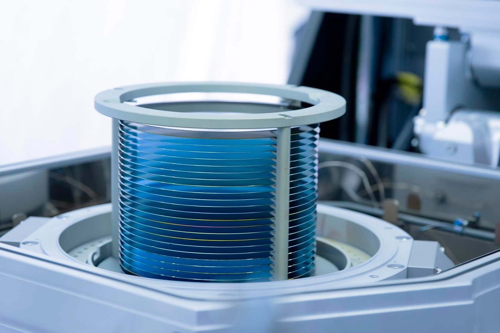
Preparation of MOF-CVD precursor layers on blanket wafer

The layers of ALD ZnO and PVD Co were prepared on highly-doped p++ Si substrates. ALD ZnO deposition was realized at 120 °C by 30 cycles of diethyl zinc (DEZ)/water precursor pulses separated by N2 purge steps (Savannah S200, Veeco Instruments Inc.). PVD Co film was sputtered on Ar-plasma precleaned Si substrate (NC7900, Canon Anelva Corp.).

Preparation of MOF-CVD precursor layer on patterned wafer

The fork–fork capacitor structures featuring 45 nm line/space width were prepared on p-type 300 mm Si-wafers according to a modified integration route (Supplementary Fig. 2) based on using sacrificial amorphous carbon (a-C) layer to form a pattern of passivated copper wires. The initial stack of layers above the substrate consisted of 1000 nm SiOx, 30 nm SiCN diffusion barrier, 90 nm a-C, and a multilayer hard-mask stack. After formation of a device pattern in the top positive resist coating with 193 nm immersion lithography, the pattern features were then transferred into the underlying a-C film. Following the wet removal of hard-mask residues, the exposed surfaces of a-C/SiCN were coated with 3 nm ALD TiN. The subsequent metallization steps included sputtering of 20 nm Cu seed, electroplating of 500 nm Cu, and chemical mechanical polishing down to the a-C film. The removal of a-C sacrificial layer was done in He/H2 remote plasma. Afterward, the metallic lines were passivated with a non-conformal 3 nm PECVD SiCN barrier layer and then additionally covered with a conformal 2 nm PEALD SiNx film. The deposition of CVD Co was realized at 200 °C on VECTOR Excel tool cluster (Lam Research Corp.). Before deposition of CVD Co on the SiCN/SiNx-passivated Cu pattern, the growth conditions were optimized on blanket SiNx surface to obtain 4.0 ± 1.0 nm Co layer across 300 mm wafer (assessed by RBS). ALD ZnO deposition on the metal lines passivated with SiNx layer was performed by applying the same growth conditions as used on blanket wafers (see above).

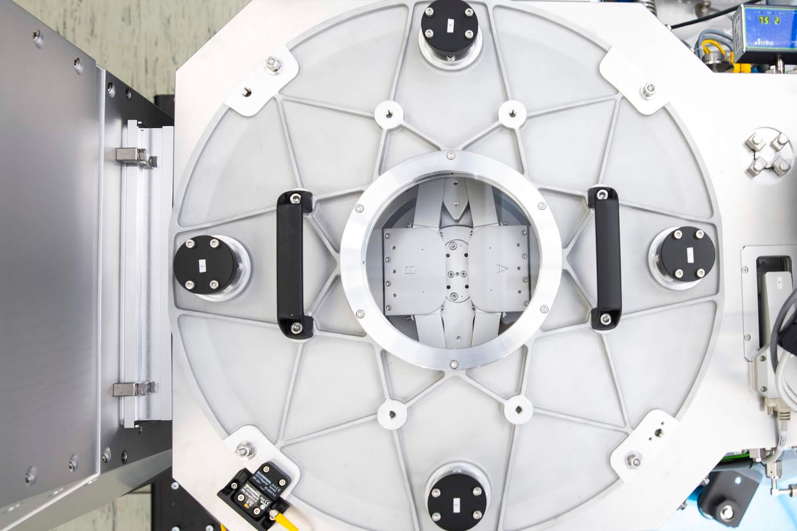
Vapor-phase conversion process (MOF-CVD)

For the conversion to appropriate ZIF layer, samples with precursor layers were placed in a glassware reactor (Supplementary Fig. 1). The glassware reactor was connected to a vacuum pump via a manual valve. Upon assembly the reactor was checked for leaks. The glass tube containing 2-methylimidazole powder (99%, CAS #693-98-1, Sigma-Aldrich) was connected to one of the ports of the glassware reactor via another manual valve. The whole setup was placed in a furnace preheated at 120 °C. After the temperature stabilization (15 min), the valve to the vacuum pump was opened, and the reactor was evacuated until pressure stabilization below 10 mbar. The vacuum valve was then closed and the valve to the 2-methylimidazole tube opened. The exposure of samples to vapors of 2-methylimidazole was set to 120 min, after which the precursor valve was closed, and the sample area of the reactor was kept under dynamic vacuum for 15 min to remove the unreacted organic linker from the sample surface and pores of formed ZIF films (activation). Finally, the reactor was let to cool down before the samples could be taken out for further characterization.
Two proposed routes for the integration of ultra-low-k MOF dielectrics in on-chip interconnects via the MOF-CVD process. Routes A and B differ in how the MOF precursor layer is formed around the interconnect wires. In Route A, metal oxide to be converted into MOF is deposited after passivation of metal lines, while Route B relies on selective conversion of metal oxide formed through controlled oxidation of the metal pattern From: Vapor-deposited zeolitic imidazolate frameworks as gap-filling ultra-low-k dielectrics
Validation of the MOF-CVD process and characterization of the deposited MOF thin films. a Schematic representation of the conversion of ALD ZnO and native CoOx to ZIF-8 and ZIF-67 and the corresponding increase in thickness as measured by spectroscopic ellipsometry (SE) and from SEM cross-sectional images. b Baseline-corrected GI-XRD diffraction patterns together with simulated powder diffractogram for ZIF-8. c Ellipsometric porosimetry with methanol and water as adsorbates. The amount of adsorbate corresponds to the change of the ellipsometric angle Delta (@633 nm) relative to the value recorded before introducing probe molecules. The values are normalized against the Delta change measured at methanol saturation pressure. d AFM topography images of MOF-CVD films: ZIF-8 (purple frame) and ZIF-67 (light blue frame) From: Vapor-deposited zeolitic imidazolate frameworks as gap-filling ultra-low-k dielectrics
Open Access This article is licensed under a Creative Commons Attribution 4.0 International License, which permits use, sharing, adaptation, distribution and reproduction in any medium or format, as long as you give appropriate credit to the original author(s) and the source, provide a link to the Creative Commons license, and indicate if changes were made. The images or other third party material in this article are included in the article’s Creative Commons license, unless indicated otherwise in a credit line to the material. If material is not included in the article’s Creative Commons license and your intended use is not permitted by statutory regulation or exceeds the permitted use, you will need to obtain permission directly from the copyright holder. To view a copy of this license, visit http://creativecommons.org/licenses/by/4.0/.