Wednesday, October 3, 2018

EREZTECH introduces Bridge Forward(TM) solution

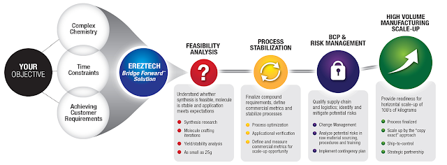
EREZTECH introduces Bridge ForwardTM solution - from synthesizing complex molecules with feasibility analysis to executing a scalable route to high volume manufacturing

Nowadays, leading technology nodes for Logic, DRAM, and NAND/3D NAND rest upon continuously increasing use of ALD & CVD in HVM. The basic layers and their applications, products and respective precursors are listed in the table below:
 
Layer Application Product Precursors (examples)
Al2O3 High-k, liner, etch stop, mask Logic, DRAM, NAND TMA, AlCl3
HfO2 High-k, mask Logic, DRAM HfCl4, TEMAHf, Hf-Cp´s
ZrO2 High-k, mask Logic, DRAM ZrCl4, TEMAZr, Zr-Cp´s
La2O3 High-k Logic La(THD)3
TiN Electrode, barrier, mask Logic, DRAM, NAND TiCl4, TDMAT, TEMAT
TaN Electrode, barrier Logic, DRAM TaF5, TaCl5, PDMAT
Co Barrier/seed, contact Logic CTTBA, CoCOCp
Ru Electrode, barrier/seed, contact Logic, (DRAM) RuCp´s, RuO4
W, WN, WC Electrode, barrier/seed, contact Logic, DRAM, NAND WF6, WCl6, W-MO

This involves a huge mix of resources including stakeholders within the fab organizations as well as external partners and suppliers from the supply chain, ranging from universities and research institutes to material suppliers, chemical and gas companies, wafer processing equipment and sub-component manufacturers, and companies facilitating R&D for the semiconductor industry.

This involves a huge mix of resources including stakeholders within the fab organizations as well as external partners and suppliers from the supply chain, ranging from universities and research institutes to material suppliers, chemical and gas companies, wafer processing equipment and sub-component manufacturers, and companies facilitating R&D for the semiconductor industry.

Few companies are capable of creating new molecules from the conception and then bringing it into HVM ; EREZTECH is one of these companies with proven track record in the semiconductor industry.

Being a single source from R&D to HVM, EREZTECH enables clients to achieve thorough control and enhanced visibility, and also helping accelerate the organometallic project. 


Leveraging the Ereztech Bridge Forward™ solution, they specialize in collaborating with results-driven clients to achieve long-term project success. From synthesizing complex molecules with feasibility analysis to executing a scalable route to high volume manufacturing.

As mentioned above, a key to success in organometallic R&D is a risk-sharing partnership. Ereztech has a network of 50+ experienced research chemists specialized in the synthesis of custom metal-organics. Having developed 500 new methods for organometallic synthesis, the EREZTECH research team continues to enrich their catalog with 800+ high purity compounds, including: 
  • Acetates
  • Acetylacetonates
  • Alkenes/Dienes
  • Carbonyls
  • Cyclopentadiene derivatives
  • Metal-alkyl and –hydride bonds
  • Phosphine 

Ereztech’s Bridge Forward™ solution is a proven process for helping clients achieve project objectives with successfully synthesizing and scaling-up complex chemicals. After developing on-demand custom precursor, their solution incorporates the following key steps:

  • Deliver 25 g of test batches for thorough review and feasibility analysis.
  • Produce pilot batches to further refine the compound to meet your purity standards and specifications.
  • Develop pre-production ramp-up, including vetting of supply chain partners and optimization of logistics
  • Produce high volumes (e.g., thousands of kilograms) of metal-organics to defined project specifications and our stringent ship-to-control standards.
After a detailed and thorough approval process, sometimes change in unavoidable - for instance, change in regulations or a replacement of a supplier.

EREZTECH stays prepared for the potential change required with their comprehensive Change Management Program that:
  • Minimizes undesirable impacts on manufacturing systems, with special care for reliability and stability of production processes.
  • Ensures the thorough technical review and accuracy of all modifications — and their test procedures — prior to making any changes.
  • Maximizes staff planning for a smooth change transition, including employee training before the change is implemented.

Recent examples of precursor scale-ups attained by EREZTECH include:

  • Scaling Up Cobalt Octacarbonyl and Its Derivatives  : LINK
  • Innovative Approach to Scaling Up Silicon Tetraiodide (SiI4) : LINK

Products – visit the EREZTECH periodic table [LINK]


Request an Ereztech Custom Synthesis [LINK]

 by Nick Kim, licensed from CartoonStock #332183

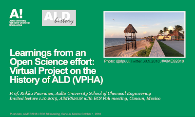
Learnings from an Open Science effort: Virtual Project on the History of ALD

Here are news from the Virtual Project on the History of ALD (VPHA) and Riikka Puurunen who is escaping the north European autumn at the ECS Fall / AiMES2018 meeting in Cancun Mexico - well deserved. VPHA is still on-going and preparations are underway to write the final review and more volunteers are still welcome!

On addition, VPHA will still like to complete the doctoral thesis list worldwide, and for this, input from ALD researchers all over the world is very much welcome - please submit your thesis!
Please follow the link for the complete presentation as preprint through ECSarXiv, : LINK

For those of you interested slide 21 for a very cool picture famous ALD-gurus and slide 27 for a proposed time line of ALD - enjoy!

R.L.Puurunen ECS AiMES 2018 Invited Talk G02-0987 Learnings from an Open Science effort: Virtual Project on the History of ALD

Screen dump from presentation available online (LINK)

Sunday, September 30, 2018

Warm welcome to India as the biggest audience of the BALD Engineering ALD Blog!

It seems that ALD is becoming a field of interest in India. Alternatively the rumor of my fantastic chicken curry and Saag Paneer has traveled further. This month India moved in to 1st position taking over the spot from USA who has held its since the start of this blog. Congratulations India! Also interesting to see that Bangladesh made it to spot 10 for the first time.

Expect more blogs on ALD in India in the near future!

Friday, September 28, 2018

SRI Intellectual form China buys Beneq from Finland

[beneq.com] Beneq® Corporation, a leading supplier of Atomic Layer Deposition (ALD) equipment and thin film coating services, and the world’s premier manufacturer of thin film electroluminescent displays, today announced a share purchase agreement about the acquisition of all Beneq Oy shares. The agreement will enable faster expansion in Beneq’s key markets and additional investments in industrial ALD thin film solutions and transparent displays.

The buyer, Qingdao Sifang SRI Intellectual Technology Co. Ltd. (SRI Intellectual), is a Chinese joint venture whose shareholders focus on rail vehicle systems and other high technology solutions.
 
 
According to the share purchase agreement, the buyer acquires all shares of Beneq Corporation (Beneq Oy) from current shareholders. The parties have agreed not to disclose the transaction price.
Accelerating the execution of Beneq’s strategy
The new investors are committed to accelerating Beneq’s strategic transformation towards industrial ALD equipment and customized and in-glass laminated transparent Lumineq displays. The agreement will allow expansion of Beneq’s sales and marketing activities, and improvements in production in Beneq’s Espoo factory, the Home of ALD.

“We are very pleased to include Beneq in our investment portfolio. Beneq is exactly the kind of high technology company with growth potential we focus on. The acquisition establishes a bridge between SRI Intellectual and Beneq that will result in a win-win situation of mutual benefits in global business development,” commented Kong Jun, Chairman of SRI Intellectual and Chairman of Beneq.

No changes in Beneq’s operations or customer projects

Beneq will continue as an independent Finnish company under the new ownership, and all existing customer projects, deliveries and agreements with customers, as well as production in Beneq’s Espoo factory will continue according to the current Beneq business plans.

“We are extremely happy to get the support of new owners that have a solid financial background and willingness to invest in the future of Beneq. The background of the investors will also give us access to new customers in interesting business growth areas, such as transparent displays and ALD solutions for the semiconductor industry,” said founder and board member Sampo Ahonen from Beneq.

Hjulbusarna at The Rally of Mälaren 22nd September


Thursday, September 27, 2018

Thermal ALE of HfO2 using HF for fluorination and TiCl4 for ligand-exchange

Until now thermal atomic layer etching (ALE) have been established by fluorination and ligand-exchange reactions using HF as fluorination reactant and Sn(acac)2, Al(CH3)3, AlCl(CH3)2, and SiCl4. Here is a new study where TiCl4 is employed as a new metal chloride reactant for ligand-exchange. 
 

In the study thermal HfO2 ALE using HF and TiCl4 as the reactants is investigated by in situ quartz crystal microbalance (QCM) measurements from 200 to 300 °C. 
 
Further, an investigation into the selectivity of thermal ALE using HF and TiCl4 revealed that HfO2 and ZrO2 were etched by HF and TiCl4 but Al2O3, SiO2, Si3N4, and TiN were not etched. This is an important finding since all of those materials are typically used in Logic High-k Metal Gate stacks and various high-k capacitor applications.
 
Please find all the details in this Open Access publication by Younghee Lee and Steven M. George from the famous ALD/ALE lab at University of Colorado, in Boulder Colorado, USA.

Thermal atomic layer etching of HfO2 using HF for fluorination and TiCl4 for ligand-exchange

Younghee Lee and Steven M. George
Journal of Vacuum Science & Technology A 36, 061504 (2018); https://doi.org/10.1116/1.5045130

10 Criteria for Gauging the Long-Term Compatibility of New Suppliers of Metalorganics

[Guest Article by Roman Rytov, CEO of EREZTECH] Even in the specifications-driven chemical commodity markets, price cannot be the sole deciding factor for the discriminating specifier of metal-organics: the stakes are simply too high.

Of course, price is a necessary qualifier. But the specifier is entering into a commitment that typically goes on for years — and decisions made early on become more tightly “locked in” at each development milestone.

This article is to help you enter into — with your eyes wide open — a highly productive relationship with a new chemical supplier. Here are 10 steps to qualify and access your new organometallics supply partner:

1. Increasingly stringent purity standards

Needless to say, your purity specifications must be met — now and forever — no matter what. In the high purity fine and specialty chemicals markets, purity can be measured out to 3, 4, or even 5 decimal places. What are their metrology capabilities?

Ask how you new supplier handles requests for higher purity standards than they’ve previously delivered. And what programs they have in place to continuously manufacture to those new, higher standards.

2. How to quantify their level of service?

Everyone says they have great service. So here are some pointed questions to ask a potential chemical supplier:
  1. How quickly can I expect your sales reps to respond to my inquiries?
  2. How knowledgeable is the sales staff about the R&D and production development process?
  3. How, specifically, will your company move from the R&D stage of the custom synthesis of metal-organics to the milestones for the required production quantities?
  4. How will any questions I have regarding compliance, accounting, packaging, and shipping be resolved?
All aspects of the business should be considered when creating an impression of the supplier: from the very first phone call to each subsequent interaction.

Wednesday, September 26, 2018

Picosun-SINANO collaboration yields excellent TiN process

ESPOO, Finland, and SUZHOU, China, 26th September 2018 – Picosun Group, a leading, global provider of ALD (Atomic Layer Deposition) thin film coating solutions, and Suzhou Institute of Nano-Tech and Nano-Bionics (SINANO) report excellent quality titanium nitride (TiN) deposited with Picosun’s plasma-ALD technology.

In microelectronic component manufacturing, the ohmic contact between metallic and semiconducting material layers is critical regarding the component functionality and lifetime. Typically, pure metals such as titanium have been employed as the metallic material, but they have certain drawbacks which is why titanium nitride has been proposed as the substitute. TiN is metallic as well, and its conductivity and thermal stability are better than those of pure titanium metal, but to obtain high quality TiN films, the manufacturing method and conditions are critical.

This is where Picosun’s remote plasma ALD (RPEALD) technology shows its strength. In Picosun’s approach, the plasma source is located on a high enough distance from the substrate, so that instead of aggressive ion bombardment, highly reactive radicals react at the substrate surface. This allows low process temperatures without thermal stress or physical ion damage to the substrate and enables deposition of also conductive materials without the risk of short-circuiting, or gas back-diffusion into the plasma source. The right selection of precursor chemicals and plasma gases guarantees high purity TiN films with very low oxygen content and work function, low sheet resistivity, exact stoichiometry, and high uniformity (*). Furthermore, the process window is wide regarding the process parameters and temperature, enabling the process to be introduced on a large variety of substrate materials. 
 
The Suzhou Institute of Nano-tech and Nano-bionics (SINANO) was jointly founded in March 2006 by the Chinese Academy of Sciences (CAS), the government of Jiangsu Province, the government of Suzhou City and the Suzhou Industrial Park. The institute occupies over 60,000 square meters of land and has 150,000 square meters of lab and office space.(LINK)

“We are happy to report these excellent TiN results to our customers in micro- and optoelectronic industries. TiN is a central material in their applications, especially in components manufactured on GaN and on small, up to 200 mm diameter Si wafers. Picosun is specially dedicated to providing cost-efficient, turn-key production solutions for up to 200 mm wafer markets. We would like to welcome you all to meet us at the 4th China ALD conference which takes place 14-17 October 2018 in the city of Shenzhen, and where we are again the platinum sponsors, to discuss further how our ALD technology could improve your products and enable new breakthroughs in your industry,” say Mr. Edwin Wu, CEO of Picosun Asia Pte. Ltd. and Mr. Jurgen Yeh, CTO of Picosun China Co. Ltd.

“It is always a pleasure to work with Picosun. The quality of their ALD equipment is outstanding and enables us to develop cutting-edge ALD processes to be introduced to our other collaboration partners in the industries. An immensely important benefit in using PICOSUN™ ALD tools is also the smooth scalability of the processes to production scale, as all PICOSUN™ ALD systems, from R&D units to full-scale industrial production platforms share the same core design and operating principles,” continues Prof. Sunan Ding from the Nano-X lab of SINANO.

SINANO and Picosun have been collaborating since the beginning of 2017. The goal of the collaboration is to develop advanced micro- and optoelectronic components such as HEMTs (high-electron mobility transistors) and laser diodes, and lithium ion batteries utilizing ALD in their joint lab in Suzhou, one of China’s most prominent hubs for electronics and other high-tech products manufacturing. The lab is equipped with several state-of-the-art PICOSUN™ ALD systems. The collaboration is further supported by Picosun’s local subsidiary, Picosun China Co. Ltd. also located in Suzhou.

Tuesday, September 25, 2018

Caltech Convert to Hollow Cathode for Better Quality Nitride Layers

[Meaglow.com] Researchers at the California Institute of Technology (Caltech) have joined a growing number of institutes that have upgraded their plasma assisted ALD system with a hollow cathode plasma source. Meaglow’s plasma sources are well known for improving nitride layers by lowering oxygen content.

One such upgrade enabled low temperature GaN thin film transistors to be deposited at 200 degrees C (see the related Applied Physics Letter). While more recent work has allowed the demonstration of superior silicon nitride layers grown for device purposes (see our earlier article). 

 
Meaglow is committed to enabling the next generation of materials development by providing deposition solutions that meet the stringent requirements of today’s researchers. See our product lines at www.meaglow.com.