Tuesday, January 10, 2017

Nanowire week in Lund, Sweden 29th May - 2nd June, 2017

10th Nanowire Growth Workshop + 9th NANOWIRES = Nanowire Week

5 days of lively discussion on all areas of nanowire research, from growth to applications

The Nanowire Week will take place in Lund, Sweden from May 29 – June 2, 2017. Nanowire Week is the merger of two well-established and highly successful annual workshops: NANOWIRES and the Nanowire Growth Workshop. Nanowire Week will cover all topics of nanowire-related research, from fabrication and fundamental properties to applications.


Abstract Deadline Feb 17 for ALD & ALE 2017 in Denver Colorado

17th International Conference on Atomic Layer Deposition
-Featuring the 4th International Atomic Layer Etching Workshop (ALE2017)- 
 
 
DATE & LOCATION:
July 15-18, 2017 Sheraton Denver, Denver, Colorado 
 
ALD 2017 will be a three-day meeting (preceded by a one day tutorial), dedicated to the science and technology of atomic layer controlled deposition of thin films. Once again the meeting will feature the Atomic Layer Etching Workshop. As in past conferences, the presentations will follow an all-electronic format, and electronic copies of the presentations will available online.

ABSTRACT DEADLINE:
February 17, 2017

WEBSITE:
Details will be posted to the ALD 2017 Website in November 2016. Bookmark: www.ald-avs.org

Monday, January 9, 2017

Researchers from the Swedish SLU & Karolinska mass produce synthetic spider silk

Some time ago MPI Halle, Germany, produced super strong spider web by coating it with ALD (Mato Knez et al). At that time the research seemed like a peculiar thing. Now however, Swedish researchers from SLU and Karoliska can mass produce synthetic spider silk at high rate and in large quantities. So all you have to do now is to integrate an ALD reactor into the machine below ...

Full story from SLU : LINK


Biomimetic spinning of artificial spider silk (figure above used with permision, SLU)
b) Photo of a fiber as it is spun in the low pH aqueous collection bath. Photo: Marlene Andersson, Swedish University of Agricultural Sciences/Nature Chemical Biology
c) Wet fiber nest in low pH buffer. Photo: Lena Holm, Swedish University of Agricultural Sciences/Nature Chemical Biology
d) As-spun fibers on a frame. Photo: Marlene Andersson, Swedish University of Agricultural Sciences/Nature Chemical Biology
Fiber diameter in (b-c) is approximately 40 micrometre and in (d) 15 micrometre. Scale bar in (a) 3cm, (b) 3 mm, and (c-d) 5 mm.


Formation of a continuous as-spun solid fiber of artificial spider silk in an acidic aqueous buffer collection bath [embedded Youtube : Published by: Anna Rising & Jan Johansson (Swedish University of Agricultural Sciences & Karolinska Institutet, Sweden)]

Friday, January 6, 2017

Functional OLEDs on Graphene electrodes by Fraunhofer FEP and Partners

Fraunhofer FEP reports that for the first time it has been shown possible to produce functional OLED electrodes from graphene. Such OLEDs can be integrated into touch displays according to the report.


  • Flexible OLED electrodes from graphene
  • The perfect material: transparent, stable, flexible, conductive
  • Ideal for touch screens, photovoltaic, wearables and much more

Above in a tweet embedded from Fraunhofer FEP an Orange luminous OLED fabricated on a graphene electrode. The process was developed and optimized in the EU-funded project "Gladiator" (12.4 M EUR - Graphene Layers: Production, Characterization and Integration) and you can find mor information here on the Fraunhofer FEP news release. Important partners where the Spanish company Graphena S.A. and British Aixtron supplier of the CVD reactor for Graphene growth.


Aixtron is offering CVD reactors for graphene and CNT growth. The AIXTRON BM systems can operate in both thermal CVD and plasma-enhanced CVD modes. The systems are based on the highly scalable showerhead concept and are available for wafer-sizes from 50mm to 300mm diameter. (aixtron.com pdf flyer)
Spanish company Graphenea S.A., which is responsible for the production of the graphene electrodes, as well as the British Aixtron Ltd., which is responsible for the construction of the production CVD reactors.

Read more at: http://phys.org/news/2017-01-milestone-graphene-production.html#jCp
Spanish company Graphenea S.A., which is responsible for the production of the graphene electrodes, as well as the British Aixtron Ltd., which is responsible for the construction of the production CVD reactors.

Read more at: http://phys.org/news/2017-01-milestone-graphene-production.html#jCp
Spanish company Graphenea S.A., which is responsible for the production of the graphene electrodes, as well as the British Aixtron Ltd.,

Read more at: http://phys.org/news/2017-01-milestone-graphene-production.html#jCp
Spanish company Graphenea S.A., which is responsible for the production of the graphene electrodes, as well as the British Aixtron Ltd.,

Read more at: http://phys.org/news/2017-01-milestone-graphene-production.html#jCp

UPDATE : CMC Conference Call for Papers, May 11-12 2017 Dallas, USA

CMC Conference Call for Papers

The Critical Materials Council (CMC) Conference Committee has issued a call for papers for presentations to be given at the CMC Conference to be held May 11-12, 2017 in Dallas, Texas, USA. Semiconductor manufacturing industry experts from IDMs, OEMS, and materials suppliers will gather to discuss actionable information on critical materials used in HVM fabs surrounding the theme of "Critical Materials for Device Driven Scaling," while also looking at issues associated with new materials needed for future devices.  
Following the annual members-only Critical Materials Council meeting to be held earlier that week, the 2017 CMC Conference is open to the public. Business drives our world, but technology enables the profitable business of manufacturing new devices in IC fabs, and new devices need new materials. In addition to panel discussions, presentation sessions will focus on the following topics:
I. Global Issues & the Supply Chain
II. Immediate Challenges of Materials & Manufacturing
III. Emerging Materials Challenges
To submit a paper for consideration, please send a 1-page abstract focusing on critical materials supply dynamics by February 10, 2017 to cmcinfo@techcet.com.
Attendees will include industry experts handling supply-chains, business-development, R&D, and product management, as well as academics and analysts. The early-bird registration fee (before April 15th) for the CMC Conference is $350; the standard registration fee is $425 (after April 16th).  CMC member companies will be attending this meeting, as it is an important part of their membership.  


On behalf of the CMC Conference Committee,
CMC Conference 2017 Registration

Registration Opens January 1, 2017
Early Bird Discount $350 (opens in January)
Standard Registration $425 
Event Sponsorship Opportunities
It is our continued goal to provide timely, relevant information on the supply-chains of critical materials through education and collaboration. None of this is possible without the help of our sponsors! For Sponsorship Opportunities, please contact Diane Scott at dscott@techcet.com.   

www.cmcfabs.org/seminars

Thursday, January 5, 2017

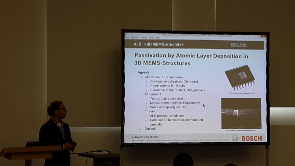
Robert Bosch to present ALD applications in MEMS manufacturing at EFDS ALD4Industry Workshop in Dresden

Dr. Florian Schön from Robert Bosch GmbH will present "ALD applications in MEMS manufacturing" at the EFDS ALD for Industry workshop in Dresden 17-18th of January 2017.  MEMS (MicroElectroMechanical Systems; Microsystems) are micrometer-scale, semiconductor-based components that combine e.g. electrical, mechanical, and optical functions. They are present in our everyday electronics in products such as hard disk read heads, inkjet printer nozzles, microphone and videoprojector chips, and airbag controls, tire pressure monitoring, and driving stability systems in cars. [Picosun, BALD Engineering]


According to the MEMS market  is lead by “MEMS Titan” Robert Bosch (Yole Développment Aug 2016) followed by STMicroelectronics and Texas Instruments.

According to the Yole Status of the MEMS Industry 2016 Report the compound CAGR from 2015-2021 for the value of MEMS markets will be 8.9%, moving from $11.9B to $20B. Over the same period the CAGR of units shipped will be 13%.


Passivation of MEMS by Atomic Layer Deposition, Matthias Schwille, Robert Bosch (ALD Lab Dresden Symposium, SEMICON Europa 2015)

After Robert Bosch, Dr. Tero Pilvi from Picosun Oy., Finland will give a talk very much related to MEMS "ALD and 3D coatings" Last year Mr. Timo Malinen, CTO of Picosun had tis to say about their ALD MEMS offering “Our MEMS customers gain immense benefits from our SEMI S2 certified PICOPLATFORM™ cluster technology. Equipped with our production-proven PICOSUN™ P-series batch ALD tools, these cluster systems have already proven their worth at the manufacturing sites of leading, global microsystems industries. Considering the MEMS market growth forecasts, propelled by the coming era of the Internet-of-Things, this product line will definitely be one of the cornerstones of our industrial ALD business".
 

Wednesday, January 4, 2017

The registration for EuroCVD - Baltic ALD in Sweden is open!

The registration fee includes admission to the conference Monday 12 June to Wednesday 14 June, conference material, lunch, coffee/tea breaks, welcome mixer Sunday 11 June, pub night on Monday 12 June and conference dinner on Tuesday 13 June.

REGISTRATION HERE!

Abstract Submission


Abstracts will only be accepted though the online abstract submission system, which will be available on November 10, 2016. The deadline for submission is January 10, 2017.

The abstract will consist of two parts: the extended abstract and the summary:

1.The extended abstract can be up to 2 A4 pages, and must follow the extended abstract template available below for download. Please download the template here (Word .docx format). Save the completed extended abstract as a .pdf for submission. Note: only .pdf files will be accepted in the online submission process.

EXTENDED ABSTRACT WORD TEMPLATE

2.The summary will be maximum 1600 character overview of the extended abstract. This should be written in as plain text as possible, with no references or figures. This summary will be pasted into a text submission box during the submission procedure.

Abstract submission closes on January 10, 2017 by midnight GMT. All abstracts should be submitted by this date. Authors will be notified of acceptance of their contributions and the type of presentation (oral or poster) by February 10, 2017.

It is important to note that the authors are solely responsible copy-editing and formatting their abstract documents. The accepted abstracts will be published as received, and any errors in formatting, spelling, grammar, or scientific content will not be corrected. If you have any technical difficulties with the submission process, please contact the organizing committee at cvdald17.abstract@meetagain.se. Other questions about the conference can be directed to henrik.pedersen@liu.se.

The scientific committee will vet the submitted abstracts, and notify the submitting author about the acceptance decision. Accepted abstracts will further be assigned as an oral or poster presentation according to the scientific committee’s decision. The two page abstract will appear in an electronic collection of abstracts distributed to the conference attendees during registration. The 1600-character summary will be published in the conference booklet. Publication of both the extended abstract and summary is contingent on registration of the submitting author.

Presenters will be notified about the scientific committee's decision by email.

SUBMIT YOUR ABSTRACT HERE

Rasirc to present New ALD chemistries for low temperature oxide and nitride films at ALD4Industry

We are very happy to announce that have received a late news abstract from RASIRC out of San Diego, USA, for a presentation to be given at the EFDS Workshop "ALD for Industry" entitled New ALD chemistries for low temperature oxide and nitride films”. RASIRC is also sponsoring the workshop and will have a stand the the exhibition.

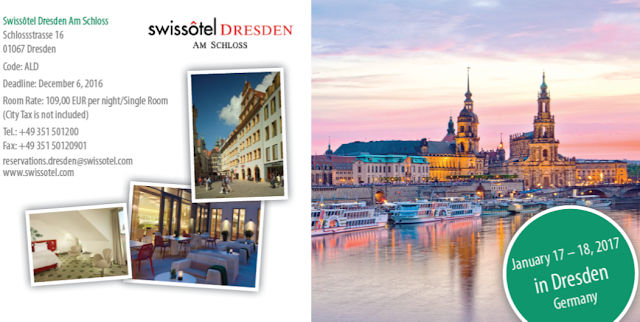
There are still room for some delegates to attend - so please consider to come to Dresden 17-18th of January and participate!


I have met Rasirc many times in Dresden and around the world. Here is a picture from Rasirc sponsoring and presenting the CMC Conference 2016 in Hillsboro USA organized by TECHCET, "Hydrazine as a Low Temperature Nitride Source: Materials Challenges for High Volume Manufacturing " at the event posing Dan Alvarez CTO and Jeff Spiegelman President and Founder.

Link to ALD fro Industry Program HERE

#ALD4Industry (follow in Twitter)

In an European context ALD was invented independently twice in Europe (Russia & Finland) and since the last 15 years Germany has grown to become one of the strongest European markets for ALD in R&D, chemicals, equipment and end users. Here, Dresden and Saxony is a unique ALD hotspot due to a strong semiconductor and equipment industry.  
 
As you can see we have managed to put together a fantastic program with representatives from the European ALD Equipment Industry : Picosun (FIN), Beneq (FIN), Sentech (GER), FHR Anlagenbau (GER), Encapsulix (FRA), ASM International (NL) and special guests from the USA  - Ultratech CNT! 
 
In addition, representatives from the chemical industry (Air Liquide), customers (Robert Bosch) and research institutions from Germany (Fraunhofer) and Finland (Aalto University and VTT Finland) will make invited and contributing talks. Topics will cover industrialization of ALD beyond the semiconductor industry:
 
▪ MEMS & Sensors ▪ Display ▪ Lightning ▪ Barriers ▪ Photovoltaics

Please visit EFDS for all information for this event and how to register HERE!


Platinum Sponsors:

logo_picosun
logo_beneqlogo_asm
logo_air-liquide

logo_fhr


Gold Sponsors:

logo_leskerlogo_strem-chemicals
logo_pegasuslogo_sentechlogo_modularflow
logo_rasirclogo_eurislogo_ultratech-cntlogo_cs-cleanlogo_ebera

Tuesday, January 3, 2017

AUO introduced bi-directional foldable AMOLED display with less than 4 mm folding radius

OLED Net reports: Taiwanese company, AU Optronics(AUO) introduced bi-directional foldable AMOLED display at IDW(International Display Workshoops) 2016 opened in Japan Fukuoka from last December 7th through 9th, which both internal and external displays can be bent 180 degrees.

The Display has an impressivily small folding radius of less than 4 mm and can endure folding cycle of more than 1.2 million times. There are no reports yet of which encapsulation technology that has been employed.

Monday, January 2, 2017

Safe garnet-based solid-state Li metal batteries using conformal ALD

COLLEGE PARK, Md. — A team of researchers at the University of Maryland Energy Research Center and A. James Clark School of Engineering have announced a transformative development in the race to produce batteries that are at once safe, powerful, and affordable. 


The researchers are developing game-changing solid-state battery technology, and have made a key advance by inserting a layer of ultra-thin aluminum oxide between lithium electrodes and a solid non-flammable ceramic electrolyte known as garnet. Prior to this advance, there had been little success in developing high-performance, garnet-based solid-state batteries, because the high impedance, more commonly called resistance, between the garnet electrolyte and electrode materials limited the flow of energy or current, dramatically decreasing the battery's ability to charge and discharge.

The University of Maryland team has solved the problem of high impedance between the garnet electrolyte and electrode materials with the layer of ultrathin aluminum oxide, which decreases the impedance 300 fold. This virtually eliminates the barrier to electricity flow within the battery, allowing for efficient charging and discharging of the stored energy.

A new paper describing the research was published online December 19 in the peer-reviewed journal Nature Materials.

“This is a revolutionary advancement in the field of solid-state batteries—particularly in light of recent battery fires, from Boeing 787s to hoverboards to Samsung smartphones,” said Liangbing Hu, associate professor of materials science and engineering and one of the corresponding authors of the paper. “Our garnet-based solid-state battery is a triple threat, solving the typical problems that trouble existing lithium-ion batteries: safety, performance, and cost.”

LEGO-style nanolayer self assembly for future logic and memory devices


Self-assembly of molecules that spontaneously form ordered phases exhibiting well-defined nanoscale periodicity and shapes may be used for future Logic, Memory and intreconnects. However, until to day these have been limited to lamellae or hexagonally packed cylinders.

A team of researchers at Brookhaven National Laboratory have recently showed how soft self-assembling materials—block copolymer thin films—can be manipulated to form a diverse library of previously unreported morphologies. The processes s modules can be repeated as an iterative self-assembly as described in the figure below.

You can read all about these exciting results it in the Open Source publication in Nature Communications: Rahman, A. et al. Non-native three-dimensional blockcopolymer morphologies. Nat. Commun. 7, 13988 doi: 10.1038/ncomms13988 (2016). 

(a) The responsive assembly strategy begins by depositing a neutral brush on the substrate of interest. A block copolymer (BCP) film is then spin-coated on the substrate and annealed to yield a well-defined morphology. Selective infiltration synthesis (SIS) is used to load one of the BCP domains with alumina; this process ‘fixes’ the thin film, making it robust and insoluble, and generates height variation between the domains. The fixed BCP film can be used as the substrate in a subsequent round of ordering. The height variation (which remains after depositing the neutral brush) templates the subsequent BCP layer, causing it to align and register in a well-defined way. Single-layer, bi-layer or multilayer inorganic replicas can be formed by ashing the film (exposure to O2 plasma), as shown in the right-most column. (b) Cross-sectional scanning electron microscopy (SEM) of an exemplar single-layer infiltrated nanostructure before and after ashing (lamellar-forming BCP, L36). (c) Cross-sectional SEM of an exemplar four-layer nanostructure. False-colour applied to highlight layers (from bottom to top): L104, L74, L36, C132. Scale bars are 100 nm. Released unde Creative Commons 4.0 from Rahman, A. et al. Non-native three-dimensional blockcopolymer morphologies. Nat. Commun. 7, 13988 doi: 10.1038/ncomms13988 (2016). 

Gallium nitride thin-film transistors produced in 200°C process by hollow cathode PEALD

Hollow cathode plasma sources, are an alternative to ICP and CCP sources and has been successfully introduced for PEALD by Meaglow Ltd. Semiconductor Today reports: Bilkent University in Turkey has developed a low-temperature process to create gallium nitride (GaN) back-gated thin-film transistors (TFTs) on flexible and rigid substrates [S. Bolat et al, Appl. Phys. Lett., vol 109, p233504, 2016]. The team reports that the "overall fabrication thermal budget is below 200°C, the lowest reported for the GaN-based transistors so far." 

According to the article in Applied Physics Letters, the GaN thin films were grown by hollow cathode plasma assisted atomic layer deposition (HCPA-ALD) at 200 °C using the popular Ultratech Cambridge Nantech Fiji PEALD system equipped with an HCP source from Meaglow. 

More information on can be found here: