Tuesday, December 13, 2016

Semiconductor Equipment Sales Forecast ─ $40 Billion

TOKYO — December 13, 2016 — SEMI, the global industry association representing more than 2,000 companies in the electronics manufacturing supply chain, today reported that worldwide sales of new semiconductor manufacturing equipment are projected to increase 8.7 percent to $39.7 billion in 2016, according to the SEMI Year-end Forecast, released today at the annual SEMICON Japan exposition. In 2017, another 9.3 percent growth is expected, resulting in a global semiconductor equipment market totaling $43.4 billion.


The SEMI Year-end Forecast predicts that wafer processing equipment, the largest product segment by dollar value, is anticipated to increase 8.2 percent in 2016 to total $31.2 billion. The assembly and packaging equipment segment is projected to grow by 14.6 percent to $2.9 billion in 2016 while semiconductor test equipment is forecast to increase by 16.0 percent, to a total of $3.9 billion this year.

For 2016, Taiwan and South Korea are projected to remain the largest spending regions, with China joining the top three for the first time. Rest of World (essentially Southeast Asia), will lead in growth with 87.7 percent, followed by China at 36.6 percent and Taiwan at 16.8 percent.

SEMI forecasts that in 2017, equipment sales in Europe will climb the most, 51.7 percent, to a total of $2.8 billion, following a 10.0 percent contraction in 2016. In 2017, Taiwan, Korea and China are forecast to remain the top three markets, with Taiwan maintaining the top spot even with a 9.2 percent decline to total $10.2 billion. Equipment sales to Korea are forecast at $9.7 billion, while equipment sales to China are expected to reach $7.0 billion.

The following results are given in terms of market size in billions of U.S. dollars:

Monday, December 12, 2016

ALD of High-k using molecular oxygen at Stanford Nanofabrication Facility

The Stanford Nanofabrication Facility (SNF) is administarting a fantastic Wiki for their clean room equipment and processeses in nanofabrication. The Wiki is there for the SNF lab community as a resource and also as historical archive as stated in the Wiki description. For all us not part of SNF it is nice that a login is not needed to view public information available.

In the wiki you will find vast process archives for the tools operated and for us ALD people the ALD section is especially interesting to study. As listed SNF is operating 4 ALD Tools all from Ultratech CNT : one Savannah and three Fiji´s.

SNF ALD Wiki  : LINK

SNF list of available films : LINK

Recently SNF published a great review of their metal alkyl amide High-k PEALD processes and the good news is that it is open source easily available for all of us to study.
 

Atomic layer deposition by reaction of molecular oxygen with tetrakisdimethylamido-metal precursor

J Provine, Peter Schindler, Jan Torgersen, Hyo Jin Kim, Hans-Peter Karnthaler and Fritz B. Prinz

J. Vac. Sci. Technol. A 34, 01A138 (2016); http://dx.doi.org/10.1116/1.4937991

Wednesday, December 7, 2016

Ultrathin protective ALD layer brings more stability to perovskite solar cell

TU Eindhoven reports: The addition of a few nanometers of a thin layer of aluminum oxide protects a perovskite solar cell against humidity – still a major stumbling block to the commercial application of this new type of solar cell. A surprising bonus is a yield boost of 3 percent. These are the findings of researchers at Eindhoven University of Technology and research institute ECN, part of the Solliance collective, published today in the journal Energy and Environmental Science.

Solar cells made from perovskite have undergone rapid development in recent years. Perovskite is a mineral that has the same crystal structure as calcium-titanium-oxide (CaTiO3). The yield of this type of solar cell has risen to 22% in just a few years. A drawback for the moment, though, is the damaging effect of humidity: water vapor from the atmosphere reacts with the perovskite crystals causing a considerable reduction in the yield over time. This instability is a stumbling block to successful commercialization.
“Although Al2O3 has electrically insulating properties, it can still be used as a buffer layer between the semi-conductive perovskite and the conductive contacts by limiting the thickness of the layer to one nanometer or less,” says FOM PhD student and first author Dibyashree Koushik (TU/e group Plasma and Materials Processing). 

Full story at TU Eindhoven : LINK

High-Efficiency Humidity-Stable Planar Perovskite Solar Cells Based On Atomic Layer Architecture

D. Koushik, W.J.H. Verhees, Y. Kuang, S. Veenstra, D. Zhang, M.A. Verheijen, M. Creatore, and R.E.I. Schropp, Energy and Environmental Science (5 december 2016). The study was co-funded by the FOM Foundation

Tuesday, December 6, 2016

Joint EuroCVD-Baltic ALD 2017: Abstract submission open!

The abstract submission for the Joint EuroCVD-BalticALD conference in Linköping, Sweden 11-14 June 2017 is now open.
 
Abstract deadline is 10 January 2017

Topics for this conference include:  
  • Precursors (design, synthesis and delivery)
  • Modelling (surface, gas phase, thermo chemistry, quantum chemistry, multi scale)
  • Process Equipment (reactors)
  • Energy Enhanced processes (Plasma, Hot wire, Photon)
  • Nanomaterials (particles, 2D-materials, nano structures)
  • In-situ monitoring (QCM, Ellipsometry, IR, syncrotron)
  • Oxides (TCO, high-k, hard coatings, thermal barriers)
  • Nitrides (semiconductors, conductors, hard coatings)
  • Carbides (hard coatings, semiconductors)Elemental films (metals, amorphous carbon)Emerging materials (hybrid MLD/ALD, sulfides)


UC Berkeley invest in Ultratech CNT Plasma ALD for Ferroelectric High-k materials research

SAN JOSE, Calif., Dec. 6, 2016 /PRNewswire/ -- Ultratech, Inc. (Nasdaq: UTEK), a leading supplier of lithography, laser-processing and inspection systems used to manufacture semiconductor devices and high-brightness LEDs (HB-LEDs), as well as atomic layer deposition (ALD) systems, today announced that the Laboratory for Emerging and Exploratory Devices (LEED), led by Professor Sayeef Salahuddin, Ph.D. of the Electrical Engineering and Computer Sciences Department at UC Berkeley (EECS UC Berkeley), has chosen the Ultratech-CNT Fiji G2 PEALD system as its instrument of choice for its research activities. Professor Salahuddin was recently honored at the White House by President Barack Obama for his work in developing nano-scale electronic and spintronic devices for low power logic and memory applications.

"ALD provides an exciting way of accessing ferroelectric materials, which play a key role in these types of devices, by providing a means of controlling the film properties through the precise engineering of the composition," noted Professor Salahuddin. "This has led the way for us to explore the ferroelectric properties of metal oxides, such as Hafnium oxide, by adding a variety of dopants, such as silicon (Si), aluminum (Al), and yttrium (Y). Our decision in choosing the Fiji system was motivated not only by the system's performance, and flexibility but also because of the strong reputation that the Ultratech ALD team has for R&D expertise, coupled with its excellent support."

Adam Bertuch, senior thin film scientist at Ultratech-CNT, who has played a key role in the development of PEALD oxides at the company, said, "The Fiji is an extremely versatile instrument, which has been at the leading edge of the development of complex materials. Professor Salahuddin's work in the field of ferroelectric materials speaks for itself, and we are looking forward to having a strong collaborative relationship with him, as well as his scientific group at UC Berkeley."

The Fiji series is a modular, high-vacuum ALD system that accommodates a wide range of deposition modes using a flexible architecture and multiple configurations of precursors and plasma gases. The result is a next-generation ALD system capable of performing thermal and plasma-enhanced deposition (LINK).

Ultratech Fiji G2 ALD System

For advanced thin films, the Fiji series is a modular, high-vacuum ALD system that accommodates a wide range of deposition modes using a flexible architecture and multiple configurations of precursors and plasma gases. The result is a next-generation ALD system capable of performing thermal and plasma-enhanced deposition. Ultratech CNT has applied advanced computational fluid dynamics analyses to optimize the Fiji reactor, heaters, and vapor trap geometries. The system's intuitive interface makes it easy to monitor and change recipes and processes as required. The Fiji is available in several different configurations, with up to six heated precursor ports that can accommodate solid, liquid or gas precursors, and up to six plasma gas lines. Options include a built-in ozone generator, Load Lock as well as several in-situ analysis tools, which offer significant experimental flexibility in a compact and affordable footprint.

Ferroelectric HfO2 at IEDM 2016

Ferroelectric HfO2 was a hot topic today Tuesday at IEDM. At 10:45 AM - A 28nm HKMG Super Low Power Embedded NVM Technology Based on Ferroelectric FETs was presented by Globalfoundries, NaMLab and Fraunhofer.


Figure form the IEDM abstract shared on LinkedIn by Prof. Thomas Mikolajick, Scientific Director at NaMLab gGmbH, Dreden, Germany.
 

Sunday, December 4, 2016

The Critical Materials Council (CMC) Celebrates 1st Anniversary

Please Join Us in Celebrating the 1st Anniversary of the Critical Materials Council as an integral part of TECHCET, formally with SEMATECH. 
 
A big "Thank you" to the original CMC members for their continued support!  


Over the course of this year, new members have been added to the CMC, including Intel, Micron, Samsung, and Broadcom. In 2017, we expect to have an even wider international presence.

In celebration, we are offering special discounts to material suppliers and fabs on CMC Membership, proceedings from the Shanghai CMC Seminar (just completed), as well as the ICPT Summaries/Proceedings. For more information, please contact Meena Sher at msher@techcet.com or go to www.cmcfabs.org/seminar

International Conference on Planarization/CMP Technology (ICPT): Beijing 2016
 
TECHCET brings directly to you a package of critical information from ICPT Beijing 2016 in the form of executive summaries on the entire event. Authored by Paul Feeney, recognized CMP veteran and technologist, the package includes a set of slides outlining the highlights of every keynote, invited, and oral talk, a hardcover copy of the proceedings, and a soft copy of the proceedings. To obtain your package for $399, please contact Meena Sher at msher@techcet.com. Please also ask about the option to have a Live Presentation and Q&A from our technologist, Paul Feeney.
 
ICPT is the world's largest conference dedicated to Planarization topics. 365 people registered to observe 117 keynote, invited, oral, and poster papers. 

 CMC Associate Membership Includes:
 
  • Critical Materials Report of your choosing, including updates throughout the year.
  • Meetings with Analysts
  • Unique Networking Opportunities!
    CMC Conference 2016
  • Discounts on CMC Conference registration
  • Ability to collectively work on issues of common concern (with CMC direction)
  • Opportunity to actively address CMC hot topics
  • ...and more!
 
Call Us For More Information! 
1-480-382-8336 ex. 101

Save The Date - 2nd Annual Critical Materials Conference May 11-12, 2017, in Dallas Texas

Save the Date for our 2nd Annual Critical Materials Conference in Dallas, Texas. Please visit our Seminars page to view the highlights from 2016. Call for Papers Starts Nov. 15.


  • Event Start Date: May 11, 2017
  • Event End Date:May 12, 2017
  • Event Venue: Dallas, Texas, USA

The Critical Materials Council is a membership-based organization collectively working toward anticipating, and solving Critical Materials Issues in a non-competitive environment by identifying/alleviating supply problems, sharing best practices, and working on industry standards for the benefit of the semi device fabrication community.


 Become a part of the Critical Materials Ecosystem!

  • Unique Networking and Active Collaboration Opportunities
  • Gain access to the latest customized supply chain news and analyst commentary
  • Receive an expertly-written Critical Materials Report Advisory of your choosing

Saturday, December 3, 2016

Russian and Finnish scientists fabricate ZnO ALD coated SWCNTs p-type field effect transistors

TASS reports: Russian scientists create carbon nanotubes coated with zinc oxide 

Researchers from Skoltech, Aalto University, and Peter the Great St. Petersburg Polytechnic University have successfully demonstrated the technique of coating zinc oxide on the surface of single-walled carbon nanotubes, the SPbPU’s press-service said. Based on the new material, ambipolar field transistors have been maintained which may find their applications in logic circuits and memory cells.

Please find the abstract below to a joint publication in Nanotechnology.


More:
http://tass.com/science/916385

Single-walled carbon nanotubes coated with ZnO by atomic layer deposition

, , , , , , , , , and

Nanotechnology, Volume 27,Number 48 

http://dx.doi.org/10.1088/0957-4484/27/48/485709

The possibility of ZnO deposition on the surface of single-walled carbon nanotubes (SWCNTs) with the help of an atomic layer deposition (ALD) technique was successfully demonstrated. The utilization of pristine SWCNTs as a support resulted in a non-uniform deposition of ZnO in the form of nanoparticles. To achieve uniform ZnO coating, the SWCNTs first needed to be functionalized by treating the samples in a controlled ozone atmosphere. The uniformly ZnO coated SWCNTs were used to fabricate UV sensing devices. An UV irradiation of the ZnO coated samples turned them from hydrophobic to hydrophilic behaviour. Furthermore, thin films of the ZnO coated SWCNTs allowed us switch p-type field effect transistors made of pristine SWCNTs to have ambipolar characteristics.

Friday, December 2, 2016

New Book - Growth and Transport in Nanostructured Materials (PVD, CVD & ALD)

Here is a good Christmas gift for the scientist you really care about.

Growth and Transport in Nanostructured Materials

Reactive Transport in PVD, CVD, and ALD

Authors: Angel Yanguas-Gil, Northwestern-Argonne Inst. of Science and Engineering, Northwestern University, Evanston, Illinois, USA 


This book will address the application of gas phase thin film methods, including techniques such as evaporation, sputtering, CVD, and ALD to the synthesis of materials on nanostructured and high aspect-ratio high surface area materials. We have chosen to introduce these topics and the different application fields from a chronological perspective: we start with the early concepts of step coverage and later conformality in semiconductor manufacturing, and how later on the range of application branched out to include others such as energy storage, catalysis, and more broadly nanomaterials synthesis. [Continue at Springer]

ASM International technical luncheon seminar in San Francisco at IEDM 2017, December 7

ASM International N.V. (Euronext Amsterdam: ASM) today announces that it will host a technical luncheon seminar in San Francisco, CA, US, on Wednesday, December 7, 2016, the third day of the IEDM Conference.


At this technology seminar ASM will highlight the challenges and potential solutions for achieving next generation 3D devices.

The agenda is as follows:

11:30 am Food and drinks

12:00 - 12:05 pm Ivo Raaijmakers (ASM) - Welcome and introduction

12:05 - 12:30 pm Invited speaker: Raghuveer Makala (SanDisk/WDC) - "Thin film deposition
challenges for 3D NAND"

12:30 - 12:55 pm Invited speaker: Jorge Kittl (Samsung) - "Perspectives on logic scaling and
implications for process requirements"

Following the presentations, there is an opportunity for open discussion and networking until 1:15 pm.

The ASM technology seminar will take place in the Golden Gate room (25th floor) at the Nikko Hotel (across from the Hilton San Francisco), San Francisco, CA 94102. The room will open at 11:30 am for invited attendees. Interested parties should contact Rosanne de Vries, +31 88 100 8569, rosanne.de.vries@asm.com.

President Obama set to block Aixtron sale

Seeking Alpha reports that President Obama is poised to block a Chinese company from buying Germany's Aixtron (NASDAQ:AIXG) because Northrop Grumman (NYSE:NOC), a major U.S. defense contractor, is among the chip equipment maker's customers.

It would mark only the third time in more than a quarter century that the White House rejected an investment by an overseas buyer as a national security risk.

Aixtron shares -6.5% in Frankfurt.


China Warns U.S. Against Blocking Aixtron Takeover

Aixtron shares fall amid U.S. national security concerns over acquisition by China’s Fujian Grand Chip Investment Fund [Wall Street Journal]

Obama bars China's Fujian from buying Aixtron's US business


The headquarters of German chip equipment maker Aixtron SE is pictured ... The Treasury Department said Obama was blocking the deal .. [Reuters]

Warum redet Amerika in der Aixtron-Übernahme mit?

Die Übernahme des deutschen Maschinenbauers Aixtron durch einen chinesischen Investor ruft die große Politik in Washi [FAZ - Frankfurter Allgemeine Zeitung]

Wednesday, November 30, 2016

The BALD Engineering ALD News Blog is growing in Asia

I am glad to see that the BALD Engineering ALD News Blog is growing in Asia. This is first month when Japan, South Korea, China and Taiwan were all on the Top 10.


Tuesday, November 29, 2016

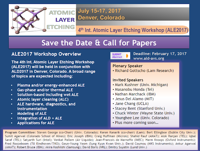
4th Int. Atomic Layer Etching Workshop ALE2017 in Denver USA July 15-17

Here is a message and update from Steve George and Keren Kanarik Co-Chairs of ALE2017:

ALE2017 will be held in conjunction with the 17th International Conference on Atomic Layer Deposition in Denver, Colorado. ALE2017 is scheduled on July 15-17, 2017. Preliminary details are posted at: https://aldconference.avs.org/.


ALE2017 will embrace many topics including:

  • Plasma and/or energy-enhanced ALE
  • Gas-phase and/or thermal ALE
  • Solution-based including wet ALE
  • Selective ALE
  • ALE hardware, diagnostics, & instrumentation
  • Modeling of ALE
  • Atomic layer cleaning (ALC)
  • Integration of ALD + ALE
  • Applications for ALE
Confirmed invited speakers for ALE2017 that will cover many of the above topics:
  • Rick Gottscho (Lam Research)
  • Mark Kushner (Univ. Michigan)
  • Masanobu Honda (Tokyo Electron)
  • Nathan Marchack (IBM)
  • Jesus Del Alamo (MIT)
  • Jane Chang (UCLA)
  • Stacey Bent (Stanford Univ.)
  • Chuck Winter (Wayne State Univ.)
  • Younghee Lee (Univ. Colorado)
ALE2017 will begin with a poster session in the evening on July 15. The plenary talks for both ALD2017 and ALE2017 are on the morning of July 16. Rick Gottscho, Executive Vice President of Global Products from Lam Research, will be presenting the ALE Plenary talk. The invited and contributed talks for ALE2017 will continue on July 16-17. In addition, there will be a networking area devoted to ALE next to the ALE posters

The abstract submission deadline for ALE2017 is February 17, 2017.


Welcome to the new web page of ALD Lab Saxony


ALD Lab Saxony is a division of Cool Silicon and combines several universities and resarch institutes to the largest German ALD cluster. Please explore our website to discover the world of Atomic Layer Deposition and to receive informations, news and announcements from the ALD community.

Please have a look on our news blog and our events section for latest information on recent activities and upcoming events.


Picosun wants you to join the ALD Powerhouse!

Picosun is the leading supplier of high quality Atomic Layer Deposition (ALD) thin film coating solutions for industrial production. Due to the growing interest towards ALD and co-operation with Picosun throughout the global industrial scene, we are constantly seeking new persons to complete our highly motivated and skillful organization. We offer you a challenging and versatile job in a dynamic, fast developing high-tech company with a supportive team and active, positive spirit.


Come to work in Picosun’s global family! We are happy to receive applications any time. Please send your open application and CV to info@picosun.com.

At the moment we are hiring for the following positions (click the titles to read more):

PICOSUN EUROPE (GERMANY)

General manager
Regional service manager

PICOSUN CHINA

General manager

PICOSUN USA

Sales manager
Regional service manager

PICOSUN FINLAND (HQ) – KIRKKONUMMI, MASALA

Process engineers
Field service engineers
Production workers
Project manager
Product manager
Mechanical designers
Purchasing manager
Production manager

 Photo, Björn Engström, Oravais, Ostrobothnia, Finland.

Friday, November 25, 2016

The ALD Passivation Market for Solar Cells is Evolving


Levitech Reports: Almere, the Netherlands – November 23, 2016 – The ongoing evolution from Al BSF cells to new PERC and n-type cell concepts will continue in the coming years. This production shift is made possible by the development of high volume capable Al2O3 deposition systems. The intrinsic properties of ALD are a perfect match with the requirements from cell design and technological point of view, both for PERC as well as n-type cells. Additionally, ALD systems result in a proven CoO benefit as compared to PECVD due to the increased maintenance interval and its beneficial effect on cell efficiencies.


从 Al BSF 电池到新型 PERC 和 n 型电池概念的持续演进将在未来的几年 中继续保 持下去。高產量 Al2O3 沉积系统 的发展推动了这一生产转变。从电池的设计 和 技 术 的 角 度 来 讲 ,无 论 是 PERC 还是 n 型电池,ALD 的固有属性可谓正应所需。除 此 之外,鉴于 ALD 系统可以增加维修间隔 并改善电池效率,它还能够带来 PECVD 不 具备的实际 CoO 益处。
 

Novel high-speed ALD outperforms current techniques for making displays

The Holst Centre in the Netherlands reports: Fast and industry-compatible, spatial atomic layer deposition (sALD) promises to revolutionize production of thin-film displays. Now researchers at Holst Centre have shown that sALD can deliver semiconductor layers with better performance than physical vapor deposition (PVD) at the same – and potentially even higher – throughputs. An easily scalable, atmospheric-pressure process, sALD could soon become the preferred method for creating large-area thin-film and flexible devices. 

 
A key step in producing next-generation ultra-high definition) displays is the creation of a highly uniform layer of an amorphous oxide semiconductor such as indium-gallium zinc oxide (IGZO). Today, this is typically done using a PVD technique known as sputter deposition. Sputtering requires expensive vacuum equipment and can also prove difficult to correctly control material composition and thickness over large areas. This results in variable transistor performance, particularly in thin film applications such as displays.

Now Holst Centre has shown that sALD offers an industry-compatible alternative which improves display performance and at the same time could cut production costs. The team has used the technique to create semiconductor layers with charge carrier mobilities (a key measure of semiconductor performance) of 30 to 45 cm2/Vs. This compares to typical mobilities around 10 cm2/Vs for sputtering. The sALD layers also exhibited low off current, switch-on voltages around 0 V and excellent bias stress stability.

"Spatial ALD offers all the performance advantages of traditional ALD – superior control of layer thickness and composition, large-scale uniformity and unparalleled conformability – but at 10-100 times the speed. So a typical 50-nm thick layer can be produced within the standard 1 minute window demanded by today's industrial processes," said Paul Poodt, Program Manager sALD at Holst Centre.

"The performance of sALD means semiconductor layers could become much thinner, enabling even higher throughputs and lower material consumption," added Gerwin Gelinck, Program Director Flexible and Large Area Transistor Electronics at Holst Centre. "In fact, its performance characteristics are preserved even when scaling down the semiconductor thickness to less than 5 nm. This can lead to novel semiconductor structures, such as super-lattices, with even higher electron mobilities."

The Holst Centre team and partners are now taking steps towards the upscaling and commercialization of these sALD processes and related equipment.

Thursday, November 24, 2016

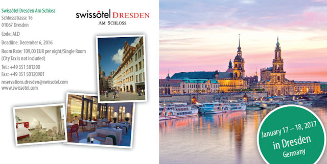
ALD For Industry kicking of the new year in Dresden

We are very happy for the interest from the ALD Equipment Suppliers and ALD Supplier Ecosystem to attend, present, exhibit and sponsor "ALD For Industry" kicking of the new ALD year 2017 in Dresden Germany 17-18th of January. 

Herzlichen Dank Ihnen allen !!!

Exhibition & Sponsoring


Link to ALD fro Industry Program HERE

#ALD4Industry (follow in Twitter)

In an European context ALD was invented independently twice in Europe (Russia & Finland) and since the last 15 years Germany has grown to become one of the strongest European markets for ALD in R&D, chemicals, equipment and end users. Here, Dresden and Saxony is a unique ALD hotspot due to a strong semiconductor and equipment industry. 
As you can see we have managed to put together a fantastic program with representatives from the European ALD Equipment Industry : Picosun (FIN), Beneq (FIN), Sentech (GER), FHR Anlagenbau (GER), Encapsulix (FRA), ASM International (NL) and special guests from the USA  - Ultratech CNT!
In addition, representatives from the chemical industry (Air Liquide), customers (Robert Bosch) and research institutions from Germany (Fraunhofer) and Finland (Aalto University and VTT Finland) will make invited and contributing talks. Topics will cover industrialization of ALD beyond the semiconductor industry:
▪ MEMS & Sensors ▪ Display ▪ Lightning ▪ Barriers ▪ Photovoltaics

Please visit EFDS for all information for this event and how to register HERE!


Monday, November 21, 2016

Sub 7nm Metrology is tough

Why the semiconductor industry needs breakthroughs, and why it’s getting tougher to provide them.

Saturday, November 19, 2016

Why is EUV so difficult and why should we ALD people care about that

Inspired by a recent article by Mark LaPedus, bad weather over Germany and coming back alive after a flue I had to return to my favorite ALD topic.  As I remember it EUV was scheduled for insertion at 32 nm and has been pushed node by node ever since then. 10 years ago when I worked at the DRAM company Qimonda (RIP) I was on a small double patterning team and at that time I got my first insights into this exciting topic and I have followed it ever since. I would say that for an ALD process engineer the HKMG stack became boring once it came into production at 45 nm. 32/28 nm let´s tune the HIG source 2 degrees Zzzzzzz. Just make up you´re mind - should we go first or last? As we care.... joking aside the three big ones, Applied Materials, Lam Research and Tokyo Electron, all failed taking control of the ALD HKMG business and this was rightfully so conquered by ASMI with a good help from Finnish and Korean ALD Technology at its finest (Microchemistry and Genitech). With respect to EUV and ALD Enabled Pattering PEALD has become a key factor and may explain partially why ASM has been successful also in that field.

Ever since ALD became part of the patterning/litho community it just feels like we are taken much more serious than when we were stuck mainly playing around with funky materials from the periodic table. In short, multiple patterning and EUV is just so much cooler! 

The situation now is that Samsung may start using EUV at 7 nm and the rest may wait until 5 nm. At least that is the current situation that I have from the last month of online media reports. That Samsung may be an early adopter for EUV maybe explained by that they have to also realize DRAM scaling sub 20 nm (more details in the article linked below).

In one sense skipping EUV has been a fantastic driver for double patterning and followed by quadruple patterning technologies realized by advanced etch processes and ALD liners. The single- and multiwafer ALD & PEALD equipment market and silicon precursor revenue volume has benefited enormously from this.

Self-aligned contact and via patterning is an established method for patterning multiple contacts or vias from a single lithographic feature. It makes use of the intersection of an enlarged feature resist mask and underlying trenches which are surrounded by a pre-patterned hardmask layer. This technique is used in DRAM cells and has been extended to patterning of active areas (see "Crossed self-aligned patterning"). It is also used for advanced logic to avoid multiple exposures of pitch-splitting contacts and vias [Wikipedia]
However, one thing that is difficult to realize with multiple patterning technology is hole patterns (described in the figure above) and here I don´t think about the regular den matrix used for e.g. DRAM cell arrays but the rather randomized pattern used for contact holes and BEOL vias. So even though you´re ALD biased at some point in time it could slow down scaling for interconnects and then that would also impact the ALD business.

So that is why it should be of interest for any ALD guy to closely follow and understand the EUV situation. Please find here some insights by Mark LaPedus at Semiconductor Engineering on what the EUV problem is all about and in great technical detail as well.

One of the most complex technologies ever developed is getting closer to rollout. Here’s why it took so long, and why it still isn’t a sure thing. November 17th, 2016 - By: Mark LaPedus, Semiconductor Engineering.

Also I can highly recommend the Wikipedia page on Multiple patterning which receives regular updates. 

To inspire you even more just take time to read this excellent review by W.M.M. Kessels et al on ALD enabled pattering: "The use of atomic layer deposition in advanced nanopatterning", Nanoscale, 2014,6, 10941-10960, DOI: 10.1039/C4NR01954G. There is definitely more to come and just maybe those holes can be made by ALD as well.


Tuning mechanical properties of ATO nanolaminates by ALD

ALD nanolaminates were first introduced in high volume manufacturing in Finland for TFEL-displays. Today even a see through version display is produced by Beneq (Lumineq). Nanolaminates have also found applications in optics by combining materials with a high difference in refractive index to tune optical properties. Also any ALD manufactured devices in the semiconductor industry can be regarded as an ALD nanolaminates like for instance the MIM stack in the DRAM capacitor cell for 90 nm and below or the HKMG stack used for transistors starting at 45 nm.

Since then, ALD nanolaminate barriers have also become technologically very important for highly flexible OLED (light-emitting diode) displays expected to go in production during 2017 for e.g. smart phone displays. Rumors in the industry say that both Samsung Electronics, LG Display and Chinese manufacturers are adopting ALD barrier production technology and that possible one of the next Iphones will have ALD barrier technology.

One of the mostly reported ALD barrier stacks consists of a repetition of a Al2O3/TiO2 bi-layer stack so called ATO nanolaminates or multilayers. These are employed to encapsulate the OLED from gas and water penetration otherwise killing the device. The key is to reduce the thickness drastically as compared to PVD or CVD barriers and thereby gaining flexibility while keeping the barrier properties for gas and water diffusion and therefore most importantly the barriers must also be pinhole free. Any pinhole will kill the diode and lead to a pixel failure. I´ve been told that a typical acceptance level for pixel failure for tablet sized displays is three (3!).


(Color online) Residual stress of the ATO nanolaminate as a function of the (a) ALD temperature, and (b) bilayer thickness. The error bars present the maximum measurement uncertainty as explained in Sec. II. © 2016 American Vacuum Society. Reproduced from J. Vac. Sci. Technol. A 35, 01B105 (2017); http://dx.doi.org/10.1116/1.4966198, with the permission of AIP Publishing and corresponding Author Oili M. E. Ylivaara
 
Until today there are not too many published reports available on residual stress, adhesion and mechanical properties in ATO nanolaminates published. Please find below the link to the Open Source publication from researchers at VTT, University of Jyväskylä and Aalto University in Finland, systematically investigating those properties as dependence from bi-layer thickness and ALD process temperature as shown above and much more. Even though the focus in this study is not on barrier properties I think there is a lot to learn here for the OLED community, especially since you operate under relatively low process temperature conditions (<100C) you must have a lot of residual stress in those flexible barriers.

Besides this report, you can also find an earlier very nice poster from Riikka Puurunen here that focuses on tuning the electrical properties of ATO nanolaminates. All this work were performed in a Picosun SUNALE(TM) R-150 reactor.

Aluminum oxide/titanium dioxide nanolaminates grown by atomic layer deposition: Growth and mechanical properties

Oili M. E. Ylivaara, Lauri Kilpi, Xuwen Liu, Sakari Sintonen, Saima Ali, Mikko Laitinen, Jaakko Julin, Eero Haimi, Timo Sajavaara, Harri Lipsanen, Simo-Pekka Hannula, Helena Ronkainen and Riikka L. Puurunen
 
J. Vac. Sci. Technol. A 35, 01B105 (2017); http://dx.doi.org/10.1116/1.4966198

Thursday, November 17, 2016

Program Released - ALD for Industry, EFDS Workshop 17-18 January 2017, Dresden, Germany

Last week we released the program for the tutorials for the  ALD for Industry, EFDS Workshop 17-18 January 2017, Dresden, Germany. Now we are very proud to release the full program for the Workshop the following day!

Link to ALD fro Industry Program HERE

#ALD4Industry (follow in Twitter)

In an European context ALD was invented independently twice in Europe (Russia & Finland) and since the last 15 years Germany has grown to become one of the strongest European markets for ALD in R&D, chemicals, equipment and end users. Here, Dresden and Saxony is a unique ALD hotspot due to a strong semiconductor and equipment industry. 

As you can see we have managed to put together a fantastic program with representatives from the European ALD Equipment Industry : Picosun (FIN), Beneq (FIN), Sentech (GER), FHR Anlagenbau (GER), Encapsulix (FRA), ASM International (NL) and special guests from the USA  - Ultratech CNT!

In addition, representatives from the chemical industry (Air Liquide), customers (Robert Bosch) and research institutions from Germany (Fraunhofer) and Finland (Aalto University and VTT Finland) will make invited and contributing talks. Topics will cover industrialization of ALD beyond the semiconductor industry:

▪ MEMS & Sensors ▪ Display ▪ Lightning ▪ Barriers ▪ Photovoltaics

Please visit EFDS for all information for this event and how to register HERE!

Workshop - Wednesday, January 18, 2017

09:00 Welcome to ALD for Industry
Dr. Sven Richter, Dr. Jonas Sundqvist, Dr. Christoph Hossbach EFDS & ALD Lab Saxony

09:20 ALD/MLD of flexible inoganic-organic hybrid thin films towards future energy harvesting and storage technologies
Prof. Maarit Karppinen; Department of Chemistry, School of Chemical Technology, Aalto University, Finland

10:00 ALD technology for the continuation of Moore’s law
Dr. Harald Profijt; Corporate R&D, ASM International, Netherlands

10:30 ALD for Life Science Applications
Dr. Ganesh Sundaram; Ultratech, Cambridge Nanotech, USA

10:50 Coffee Break

11:20 Solid precursors for ALD: challenges and opportunities
Dr. Nicolas Blasco; Air Liquide, France

11:40 ALD for optics
Dr. Adriana Szeghalmi; Friedrich-Schiller-Universität Jena, Institute of Applied Physics, Germany

12:00 Opportunities, challenges and solutions for ALD thin-film encapsulation in flexible electronics applications
Dr. Mikko Söderlund; Beneq Oy., Finland

12:20 Lunch Break

13:20 Industrial deployment of nano-engineered ultrabarriers for encapsulation of organic electronics
Dr. Jacques Kools; Encapsulix S.A., France

13:40 ALD applications in MEMS manufacturing
Dr. Florian Schön; Robert Bosch GmbH, Germany

14:00 ALD and 3D coatings
Dr. Tero Pilvi; Picosun Oy., Finland

14:20 Thin films in 3D structures: metrology with microscopic lateral high-aspect-ratio structures
Mikko Utriainen; VTT Technical Research Centre of Finland Ltd., Finland

14:40 Coffee Break

15:00 Where no man has gone before - unique equipment enables unique research
Dr. Hannes Klumbies; FHR Anlagenbau, Germany

15:20 ALD systems for no damage, high uniformity and stability of multilayer deposition
Dr. Hassan Gargouri; SENTECH Instruments GmbH, Germany

15:40 ALD process optimization by equipment simulation
Dr. Jörg Schuster; Fraunhofer ENAS, Germany

16:00 Closing remarks and discussion
Dr. Sven Richter, Dr. Jonas Sundqvist, Dr. Christoph Hossbach
EFDS & ALD Lab Saxony

16:20 End of Workshop Day
 

Wednesday, November 16, 2016

Oxford Instruments Plasma Technology free webinars

Oxford Instruments Plasma Technology has a new media centre that has just gone live, allowing you unlimited access to their on-demand webinars, videos and more!

The two most recent webinars:

Growth and Characterisation of 2D Materials Beyond Graphene
Dr Ravi Sundaram, Oxford Instruments & Dr Tim Batten, Renishaw

SiC Via Etching for RF Devices
Oxford Instruments Plasma Technology 

Lam Research Tech brief on Atomic Layer Etching - ALE


Lam Research has just published a great Tech Brief covering Atomic Layer Etching on their Blog (Tech Brief: All About ALE ). Thanks Terry Francis for sharing this one!

The article covers the following:
  • Plasma Etch Basics
  • Plasma Etch Challenges
  • Atomic Layer Etching
  • Benefits of ALE
  • Growing Need for ALE

References


Tuesday, November 15, 2016

Special Issue: Atomic Layer Deposition for Energy and Environmental Applications

Here is a Special issue in Advanced Materials Interfaces: Atomic Layer Deposition for Energy and Environmental Applications LINK. The issue is guest edited by Neil P. Dasgupta, Liang Li, and Xueliang Sun.

The ALD Energy and Environment special issue has 11 invited research articles and 5 review articles  from leading ALD experts. The focus is on the following applications:
  • photo-voltaics
  • batteries
  • supercapacitors
  • photoelectrochemical cells
  • transparent electrodes
  • sensors
  • environmental barrier layers. 
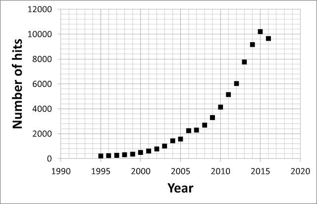
The editors argue that ALD for Energy, judging by the number of publications the last 15 years (Web of Science database) is one of the faster growing application fields. Since we have a christian holiday tomorrow in Saxony I had some time to make a plot based on Google Scholar, which includes also patents. Yes you can see exactly the same growth trend. So folks ALD and Energy is coming and that is why you should check it out below (Embedded Twitter link to the journal).

Google Scholar year by year for "atomic layer deposition" AND energy. Obviously energy can also be used for binding energy etc. but I think the message is clear.

Monday, November 14, 2016

Tutorial on Fast Spatial Atmospheric ALD by David Muñoz-Rojas from LMGP-CNRS

We are happy that Dr. David Muñoz-Rojas from LMGP-CNRS, Grenoble will come to Dresden in January 17th 2017 to give a Tutorial at ALD for Industry on Spatial ALD "Speeding up the unique assets of ALD". Until then please enjoy this recent presentation available on Youtube - pretty amazing stuff!


Dr. David Muñoz-Rojas - Laboratoire des Matériaux et du Génie Physique (LMGP) Université Grenoble Alpes, Grenoble, France - presents a Waterloo Institute for Nanotechnology (WIN) seminar titled: "Atmospheric Pressure Spatial Atomic Layer Deposition (AP-SALD): a new technique allowing the fast and scalable “printing” of functional oxides" (Embedded Youtube)


Aalto University present light detector with record-high sensitivity that may revolutionize imaging

Aalto University has presented a new light detector with record-high sensitivity that may revolutionize imaging. The research team led by Prof. Hele Savin claim that that the new light detector can capture more than 96 % of the incoming photons from visible, ultraviolet through to infrared wavelengths. The key feature is a nanostructured antireflection without limitation to specific wavelengthe or incident angle.
You probably guessed it by now - yes the new detector uses ALD - an inversion layer deposited by ALD.
"We also addressed electrical losses present in traditional sensors that utilize semiconductor pn-junctions for light collection. Our detector does not need any dopants to collect light - instead we use an inversion layer generated by atomic layer deposited thin film."

Read more at: http://phys.org/news/2016-11-detector-record-high-sensitivity-revolutionize-imaging.html#jCp

Read more in this news release by Aalto University : LINK

The Plasma ALD Guy presented the latest PEALD statistcs at AVS 63 in Nashville

The Mysterious Plasma ALD Guy presented the latest PEALD statistcs at AVS 63 in Nashville:

Saturday, November 12, 2016

Tutorials on Atomic Layer Deposition in Dresden Jan 17, 2017

ALD Lab Saxony, IHM TU Dresden, Fraunhofer IKTS and EFDS invites you to visit Dresden January 17-18 to learn the latest in ALD processing, technology and applications as part of the EFDS ALD for Industry Workshop. After the tutorials there will be an opportunity to visit ALD labs and clean rooms at the Technical University Dresden (IHM and NaMLab) and Fraunhofer Institute for Ceramic Technologies and Systems IKTS.


The 2nd day will be the main workshop day with invited talks from leading researchers and industry experts on the broad range of topics. The workshop will focus on non-Semiconductor industrial applications of today and the emerging markets with an expected industrialization in the next 5 years. Presentations will focus on the latest topics and the state of the art in the field of Atomic Layer Deposition. In parallel there will be an exhibition, giving great opportunities for face to face meetings and to share product information. The workshop will provide an excellent platform for discussions and networking during the program as well as during the social events.

More information will follow!

Tutorial - Tuesday, January 17, 2017

12:30 Introduction and fundamentals of ALD
Prof. Johann W. Bartha; IHM, TU Dresden, Germany

13:00 ALD of metals
Dr. Colin Georgi; Fraunhofer ENAS, Germany

13:30 Overview of ALD equipment and technologies
Dr. Christoph Hossbach; IHM, TU Dresden, Germany

14:00 Coffee Break

14:30 Speeding up the unique assets of ALD
Dr. David Muñoz-Rojas; LMGP-CNRS, Grenoble

15:00 In situ metrology techniques in ALD
Marcel Junige; IHM, TU Dresden, Germany

15:30 ALD applications, equipment and precursor market outlook 2017 to 2020
Dr. Jonas Sundqvist; Fraunhofer IKTS, Germany / Techcet LLC, USA


Welcome to Dresden from ALD Lab Saxony!

Friday, November 11, 2016

Abstract submission is now open for the joint EuroCVD 21 - Baltic ALD 15 meeting in Linkoping, Sweden (June, 2017)

Abstract submission is now open for the joint EuroCVD 21 - Baltic ALD 15 meeting in Linkoping, Sweden (June, 2017):


Abstract Submission

Abstracts will only be accepted though the online abstract submission system, which will be available on November 10, 2016. The deadline for submission is January 10, 2017.

The abstract will consist of two parts: the extended abstract and the summary:

1.The extended abstract can be up to 2 A4 pages, and must follow the extended abstract template available below for download. Please download the template here (Word .docx format). Save the completed extended abstract as a .pdf for submission. Note: only .pdf files will be accepted in the online submission process.

2.The summary will be maximum 1600 character overview of the extended abstract. This should be written in as plain text as possible, with no references or figures. This summary will be pasted into a text submission box during the submission procedure.

Abstract submission closes on January 10, 2017 by midnight GMT. All abstracts should be submitted by this date. Authors will be notified of acceptance of their contributions and the type of presentation (oral or poster) by February 10, 2017.

It is important to note that the authors are solely responsible copy-editing and formatting their abstract documents. The accepted abstracts will be published as received, and any errors in formatting, spelling, grammar, or scientific content will not be corrected. If you have any technical difficulties with the submission process, please contact the organizing committee at cvdald17.abstract@meetagain.se. Other questions about the conference can be directed to henrik.pedersen@liu.se.

The scientific committee will vet the submitted abstracts, and notify the submitting author about the acceptance decision. Accepted abstracts will further be assigned as an oral or poster presentation according to the scientific committee’s decision. The two page abstract will appear in an electronic collection of abstracts distributed to the conference attendees during registration. The 1600-character summary will be published in the conference booklet. Publication of both the extended abstract and summary is contingent on registration of the submitting author.

Presenters will be notified about the scientific committee's decision by email.