Thursday, July 21, 2016

Signed the contract to supply ALD equipment to Chinese DMEGC for high efficiency solar cells

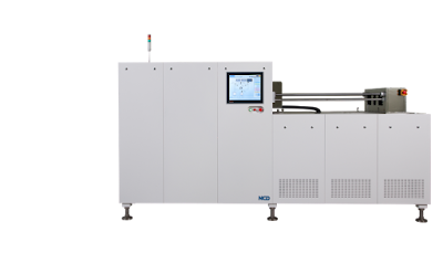
NCD has just contracted with Chinese DMEGC to supply solar cell manufacturing equipment which would produces over 100MW. This equipment is Lucida GS Series ALD system for mass-producing high efficiency crystalline solar cell using Al2O3-ALD passivation to reduce surface defects on the rear side of wafers. This is paramount achievement because it is export of mass production equipment to China of the Mecca of solar cell production through winning against big international competitors. The production capability of this equipment has been improved through our a lot of production experience comparing to the previous systems. It certainly shows that the customer has proved the technology of NCD and the excellence of the equipment, and NCD would make it the most memorable turning point for our future oversea sales.

Lucida™ GS Series ALD
High throughput atomic layer deposition system for surface passivation of c-Si solar cells


Lucida™ GS series

Lucida™ GS series + Automation


Applications
·         Al2O3 surface passivation of c-Silicon solar cells
·         Applications of mass-production
·         Industrial fully-automated production equipment
·         High throughput : up to 3400 wafers/hour of 156 x 156
Features
·         Al2O3 thin films with good thickness uniformity
·         Advanced process kit and small volume chamber for short gas cycle times
·         Extremely materialize ALD mechanism
·         Small foot print
·         Totally integrated process module
·         Easy process control
·         Automatic cassette to cassette operation
Technical specifications

Model
Material
Wafer size
(mm2)
Thickness
(nm)
Throughput
(wph)
Lucida™ GS800
Al2O3
156x156
10
>1700
Lucida™ GS1200
Al2O3
156x156
10
>2400
Lucida™ GS1600
Al2O3
156x156
10
>3400


Ultratech CNT in Dublin at ALD2016 presenting latest work on Superconductivity, SAMS Area-Selective ALD (ASD), Molybdenum Nitride and product developments

The Platinum Sponsor, supporting over 450 ALD research systems worldwide, will bring its science team to the ALD conference to present latest work and discuss leading edge application developments with delegates. Available at booth #15 and presenting as follows.


Plasma enhanced atomic layer deposition of molybdenum nitride
Adam Bertuch*1, Brent Keller2, Ganesh Sundaram1, Jeffrey Grossman2
1Ultratech - Cambridge NanoTech, USA, 2Department of Material Science and Engineering, Massachusetts Institute of Technology, USA
Tuesday 26 July:  Plasma-enhanced deposition and etching  -  Tuesday 26 July 15:45-17:15
16:30-16:45
Controlling smoothness of thin platinum ALD films
Ritwik Bhatia*1, Ralf Heilmann2, Alexander Bruccoleri3, Brandon Chalifoux2
1Ultratech-Cambridge Nanotech, USA, 2Massachusetts Institute of Technology, USA, 3Izentis LLC, USA
Wednesday 27 JULY:  Noble metals  -  Wednesday 27 July 08:15-10:15
10:00-10:15
Plasma enhanced atomic layer deposition of superconducting NbN films
Mark Sowa*1, Yonas Yemane2, J Provine3, Fritz Prinz4
1Ultratech/CNT, USA, 2Stanford University, Department of Applied Physics, USA, 3Stanford University, Department of Electrical Engineering, USA, 4Stanford University, Department of Mechanical Engineering and Department of Materials Science and Engineering, USA
Tuesday 26 July:  Poster session 2  -  Tuesday 26 July 17:15-19:00


Sunday, July 17, 2016

The 3rd International Conference on ALD Applications & 2016 China ALD Conference

Following the successes of the previous two international Conferences on ALD Applications and China ALD Conferences since 2010, the 3rd International Conference on ALD Applications & 2016 China ALD Conference will be a four-day meeting, dedicated to the fundamentals and applications of Atomic Layer Deposition (ALD) technology in various fields. It will be held in Suzhou, China, from October 16 to 19, 2016. This conference will feature plenary sessions, oral sessions, poster sessions and industrial exhibitions.

 
Please submit your abstract for Oral or Poster presentation to the email address: cald@fudan.edu.cn by 31 August 2016. Preregistration opens on 15 July 2016.

For more information, please visit the C-ALD website: http://www.c-ald.com/

Organizing Committee chairs: 
 Prof. Shi-Jin Ding, Fudan University (sjding@fudan.edu.cn
Prof. Yongfeng Mei, Fudan University (yfm@fudan.edu.cn
 

2016 General meeting of HERALD at ALD Conference

The 2016 general meeting of the HERALD COST Action MP1402 will take place during the 16th International Conference on Atomic Layer Deposition, which is taking place in the Convention Centre Dublin, Ireland, on 24th-27th July 2016. The final morning of the conference is being devoted to HERALD, in parallel with other conference sessions.

27th July 2016, Liffey Hall 1:

8:45-10:15 HERALD Showcase: Presentation by working group leaders of scientific collaborations in each WG, with opportunity for discussion from all members. Discussion of HERALD targets for widening participation and structuring the ALD community in Europe in the future.

10:15-11:00 HERALD Poster Session: Opportunity for all members to display and discuss posters. There will be no review or selection of abstracts, but the intention to display a poster must be indicated via registering on the eventbrite page by 13th July.

11:00-12:30 Launch of HERALD White Paper on 'Atomic-level processing' and panel discussion: A panel discussion on the future of atomic-level processing for European manufacturing, and in the global context. All are welcome to attend and put their questions to the panellists.

The HERALD sessions are open to all delegates of the ALD2016 conference at no extra fee. HERALD members are strongly encouraged to attend. Travel reimbursements through HERALD are not available, except for the collaboration competition that was previously advertised.


Please register your intention to attend part or all of the HERALD sessions via this eventbrite page by 13th July, so as to facilitate seating, catering and poster boards:

https://www.eventbrite.com/e/herald-sessions-at-ald2016-ireland-tickets-26329089014

The password for the eventbrite page is HERALD 

Tuesday, July 12, 2016

Oxford Instruments to present recent developments in ALD and ALE in Dublin at ALD2016

Oxford Instruments, a company that truly master both Atomic Layer Deposition and Atomic Layer Etching, will be giving two talks at the Joint ALD2016 Conference and ALE2016 Workshop in Dublin, Ireland in less than two weeks. Naturally one on each topic!

Oxford Instruments is Platinum sponsor of the conference and you will have an opportunity to meet with their Deposition and Etch Experts at the Exhibition and Social events.

Harm Knoops
Oxford Instruments Plasma Technology, UK / Researcher at TU Eindhoven, NL
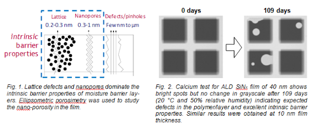
Low-temperature plasma ALD of silicon nitride moisture barrier layers

Wednesday 27 JULY: Silicon-based materials - Wednesday 27 July 14:00-15:30
15:15-15:30

ALD has demonstrated to be able to provide excellent moisture barrier layers, which are vital for the encapsulation of organic (opto-)electronic devices, such as organic light-emitting diodes (OLEDs) and thin-film photovoltaic cells. Very low water vapor transmission rates (WVTR) have been shown using oxide layers prepared by ALD (Al2O3 and TiO2) but not yet for nitride layers. In this work, moisture permeation barrier layers of SiNx prepared by ALD using SiH2(NHtBu)2 (BTBAS) precursor and Ar-N2 plasma were investigated.1 Intrinsic WVTR values in the range of 10−6 g/m2/day were obtained, indicating excellent barrier properties for ALD SiNx layers as thin as 10 nm.


Mike Cooke, CTO
Oxford Instruments, UK
Atomic layer etching (ALE) in close-to-conventional plasma etch tools

Tuesday 26 July: Plasma-enhanced deposition and etching - Tuesday 26 July 15:45-17:15
15:45-16:15

Plasma etching equipment and expertise is widespread, and cyclical etch processes are well known for high rate silicon etching. With the recent surge in interest in atomic layer etching, many groups are attempting to perform ALE in their existing tools. This talk discusses the limitations and options of using conventional tools for ALE, and gives results for both conventional and modified equipment.


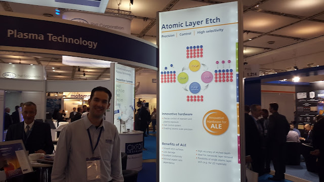
Oxford Instruments releasing new innovative hardware for ALE (Atomic Layer Etching) Harm Knoops at SEMICON Europa 2015, Dresden, Germany.
In addition, you may be interested in talk given by Dmitry Suyatin on III/V Nanowire splitting by ALE - work all performed on an Oxford Instruments Plasmalab 100 at Lund Nano Lab, Sweden

Dmitry Suyatin
Staff Engineer, Lund Nano Lab, Lund University, Sweden
Monday 25 July, Monday 25 July 13:45-15:15
Liffey Hall 1
Workshop: Non-traditional ALE approaches

To study the ALE process for III/V nanowires GaP nanowires were grown by metal organic vapor phase epitaxy (MOVPE) from gold seed particles on GaP substrates and then mechanically transferred to Si surface. An ALE process optimized for Si etching was used to etch the GaP nanowires by applying a 30 nm (105 cycles) etch recipe. Surprisingly, we discovered that we were able to split the nanowires longitudinal into too wires (as shown in Figure 1, below).


Meet Picosun at ALD2016 Ireland and join the PicoParty(TM)

Picosun is announcment: Meet #Picosun at Stand #40 at #ALD2016_Ireland! Claim your gift, win an iPad - and don't forget the PicoParty™!

Monday, July 11, 2016

ALD 2016 panel discussion atomic-level processing

At this years ALD Confernce in Ireland there will be a panel discusion a panel discussion on the future of atomic-level processing for European manufacturing, and in the global context. The discussion is co-hosted by the HERALD COST Action, but all are welcome to attend and put their questions to the panellists. 

As important background information you are all very much welcome to download the white paper "The future of atomic level processing" written by Simon Elliott, Co-Chair of ALD2016 and initiator and Chair of the HERALD COST Action.
Executive Summary
Atomic-level control of materials processing will be needed in the semiconductor industry within the next 5-10 years, and will be a powerful enabling technology for other high-tech manufacturing sectors. This will be possible if atomic-level precision can be achieved with the traditional fabrication steps – deposition, patterning and etching. There is therefore a strong need for coordinated research now into how the current concept of atomic layer deposition may be developed into selective-area patterning and atomically controlled etching.


White Paper download: LINK

The panel will be moderated by Jonas Sundqvist, co-chair of ALD2016 and the current panel members are:
  • Dr. Suvi Haukka, ASM Microchemistry, Finland
  • Dr. David Thompson, Applied Materials, USA
  • Dr. Jean-Marc Girard, Air Liquide, France
  • Prof. Mikko Ritala, University of Helsinki, Finland
  • Prof. Fred Roozeboom, Eindhoven University of Technology / TNO - Solliance, The Netherlands"

PLEASE SUBMIT YOUR QUESTIONS TO

Chair: Jonas Sundqvist (jonas.sundqvist@baldengineering.com)
Link: LINK


Applied Materials Releases Selective Etch Tool - The Producer® Selectra™ Etch system

As reported by By Ed Korczynski, Sr. Technical Editor Solid State Technology : Applied Materials has disclosed commercial availability of new Selectra(TM) selective etch twin-chamber hardware for the company’s high-volume manufacturing (HVM) Producer® platform. Using standard fluorine and chlorine gases already used in traditional Reactive Ion Etch (RIE) chambers, this new tool provides atomic-level precision in the selective removal of materials in 3D devices structures increasingly used for the most advanced silicon ICs. The tool is already in use at three customer fabs for finFET logic HVM, and at two memory fab customers, with a total of >350 chambers planned to have been shipped to many customers by the end of 2016.

Fulls story : http://semimd.com/blog/2016/06/29/applied-materials-releases-selective-etch-tool/


Full information as released by Applied Materials can be found here : http://www.appliedmaterials.com/products/producer-selectra-etch

 
The Producer® Selectra™ Etch system introduces unprecedented capabilities for sustaining the momentum of Moore’s Law through further scaling of 3D logic and memory chips. This process can remove target materials with unprecedented selectivity to one or more films. (appliedmaterials.com)

Dublin, Ahoy! Beneq will be everywhere at ALD2016

As promoted by Beneq - The ALD event of the year is approaching. As you know, Beneq is a platinum sponsor of ALD 2016 (the 16th International Conference on Atomic Layer Deposition), which will be held at the Convention Centre Dublin, Ireland, 24-27, July 2016. 
If you are coming to the event (it is not too late too book!), you can find us everywhere at the event: we will have a stand at the exhibition, we have several presentations in the conference, and we will have a large event team you can book meetings with.

Meet us at the Beneq ALD Boat Bar

This year, there is also a new attraction: The Beneq ALD Boat Bar. It will be our meeting room, lounge area and the heart of the best ALD discussions. The bar will be open every day of the event (Monday through Wednesday) in the White Bar of MV Cill Airne, right next to the convention centre.

You are cordially invited to join us for a pint on board. We believe that the discussions at our boat bar will be what this year’s ALD conference will be remembered for. Get in touch with your favorite Beneq person to get your personal invitation!

Meet us at Booth number 30

The conference also comprises an ALD exhibition. On the Beneq stand, we will have many interesting ALD objects on show, from the latest research samples to a selection of ALD coated end products.

This is also where you can get more information about the multitude of ALD applications we have been working with and all our latest products (stay tuned for more exciting product news before the event!). The number of the Beneq booth is 30. Come and take a look.

Meet us in Beneq presentations at ALD2016

The Beneq team also has several presentations in conference program. Here are the details:

1) Sami Sneck will be speaking in the session Transparent conductive oxides and optical applications 1 in the morning of Wednesday July 27th. His presentation is about Development of the world's most transparent display - enabled by ALD.

2) Mikko Söderlund will be presenting about Large area sheet-to-sheet spatial ALD system for high-throughput coating applications in poster session 2 on Tuesday 26th of July.

3) In the same poster session, also Kari Härkönen from our Development Services team will be presenting. His topic is ALD-based 3D NIR filter and refractive index control for Rugate filters.

We are all set and ready to board. See you in Dublin!

Sunday, July 10, 2016

MSP´s Ultra High Purity Vapor Filtration For Semiconductor ALD And CVD Applications

As reported by MSP : MSP’s ultra-high efficiency semiconductor Vapor and Process Gas (VPG) filters achieve the highest filtration industry efficiency rating, twelve 9s or 99.9999999999% at 2.5nm, for semiconductor application. VPG filters remove particles from low pressure, high temperature gas/vapor mixtures for use in atomic layer deposition (ALD) and chemical vapor deposition (CVD) applications.


The Model 2920 VPG Filter™ is an ultra- high efficiency filter designed for Vapor and Process Gas filtration. The VPG Filter has an estimated particle penetration of less than one part per trillion and a filter efficiency of 99.9999999999% (twelve 9s) at 2.5 nm. This 2.5nm, part-per-trillion particle penetration, twelve-9 efficiency rated filter is the highest rated filter in the filtration industry for semiconductor applications.

Conventional high-purity, point-of-use gas filters are used in a compressed gas line for particle removal. In contrast, the VPG™ filter is generally used downstream of a vaporizer under vacuum flow conditions to remove particles from a gas/vapor mixture with the carrier gas—such as nitrogen, argon or helium—being mixed with a chemical precursor vapor containing hafnium, zirconium, or other elemental species of interest for atomic layer deposition (ALD) as well as chemical vapor deposition (CVD) applications.

FILTER EFFICIENCY

The particle removal efficiency of a compressed gas filter can be determined directly by counting particles upstream and downstream of a filter by a laser particle counter, or a condensation particle counter. The efficiency of a vapor and process gas filter can only be determined indirectly by particle counting using an inert gas that is compatible with the particle counter used for the test. The measurement results can then be extended to cover conditions similar to those encountered in the actual process through mathematical modeling.

For vapor/ process gas mixture filtration, the filter may be exposed to operating pressures as low as 10 Torr, temperatures as high as 300C, and chemically reactive vapor in the mixture. Direct filter efficiency measurement is generally impossible. Experimental measurement with mathematical extension provides an alternative.

MSP has developed a predictive model to extend the test result obtained by a condensation particle counter under normal room temperature and pressure conditions into the vacuum flow conditions of the VPG filter in a semiconductor thin film deposition tool.

For the VPG-A3 filter the particle penetration is 1 x 10**6, or 1 part per million at 100nm. At 10nm, the penetration is 1 part per billion. At the lower detection limit of the condensation particle counter of 2.5 nm, the penetration is less the 1 part per trillion. The filter efficiency is thus 99.9999% (six 9s) at 100nm, 99.9999999% (nine 9s) at 10nm, and 99.9999999999% (twelve 9s) at 2.5nm.

MSP research shows that the VPG-A3 filter is an ultra-high efficiency filter capable of removing almost all particles from a gas/vapor mixture stream from 2.5nm to 100nm. In filtration, the term “absolute filter” is generally used for filters with a particle penetration that is too low to detect. The VPG-A3 filter is therefore an Absolute Nano-Particle Filter™, capable of removing substantially all nano-particles from 2.5 nm to 100 nm to a very low and essentially non-detectable level. This 2.5nm, part-per-trillion penetration, twelve 9 efficiency filter is the highest rated filter for [vapor/process gas filtration in the semiconductor industry.

PRESSURE DROP, OPERATING LIFE, AND FILM THICKNESS UNIFORMITY

The particle removal efficiency is but one of several filter characteristics for vapor/process gas filtration. Other important characteristics include the filter pressure drop, the filter life, and the physical design of the filter that can influence the film thickness and its uniformity. All these factors are taken into consideration in the design of the VPG family of filters from MSP to insure reliable operation and long service life under the most demanding process environment in semiconductor film deposition processes.

Updates and information for ALD 2016 Conference – 24 – 27 July in Dublin, Irleand

Here are some recent updates and information for ALD 2016 Conference – 24 – 27 July.


Speakers and Conference Programme

The conference programme for the the conference can be viewed here.

Delegate Information

Delegate information detailed here to help you plan your visit to Dublin: 
http://ald2016.com/delegate-information/

Poster printing:

Details regarding the format for printing can be found here:  Poster Printing Instructions for ALD2016.  Please note that all authors are required to print their own posters and the document includes details of a local company that is located close to the Convention Centre.

ALD2016 Exhibitors

Information regarding set up at The CCD and conference information can be found here: http://ald2016.com/exhibition-information/

SoLayTec launches new product and proves cell efficiency gain of 0,2% compared to PECVD AlOx

During the last two exhibitions, new products of Tempress and SoLayTec were revealed. Especially for the next PERC2.0 expansions those products are highly requested by the market. The 2nd Generation InPassion ALD combined with the newest direct PECVD can annually produce up to 130MW including the integrated anneal process.

The 2nd Generation InPassion ALD combined with the newest direct PECVD can annually produce up to 130MW including the integrated anneal process.
The SoLayTec ALD technology is based on spatial separation of precursor gasses instead of time based separation. The different gasses are confined in specific process areas while the wafers pass by. Every point on the wafer is sequentially in contact with the wafers. This creates  the (real) ALD effect and reaction. - See more at: http://www.solaytec.com/technology/spatial-ald#sthash.09CPLKVy.dpuf

SoLayTec InPassion ALD process module with a Field Replaceable process unit (www.solaytec.com)
Field Replaceable Un()
The SoLayTec ALD technology is based on spatial separation of precursor gasses instead of time based separation. The different gasses are confined in specific process areas while the wafers pass by. Every point on the wafer is sequentially in contact with the wafers. This creates  the (real) ALD effect and reaction. - See more at: http://www.solaytec.com/technology/spatial-ald#sthash.09CPLKVy.dpu
 
Furthermore, two weeks ago the 25th Intersolar exhibition and EUPVSEC conference were held in Munich. In several presentations the InPassion ALD was an important topic. Research institute Imec presented its latest results regarding n-type IBC cells on 156x156mm2 using Al2O3 from SoLayTec. Furthermore Hanwha Q Cells presented its evaluation results of InPassion ALD versus MW-PECVD and SoLayTec gave an overview of its successful PERC integration project of one of their key customers.

PERC2.0

“For PERC integration the Al2O3 ALD machine only, is not the complete solution. A customer also needs a PECVD capping machine for covering the Al2O3 layer. So far a customer needed at least 6 direct PECVD tubes to meet the ALD output of 3600wph. Since 10th SNEC exhibition in Shanghai Tempress introduced the SPECTRUM PECVD which has at least the same nett capacity as the InPassion ALD. So now capex wise we have a highly cost effective solution available for our customers”, said Roger Görtzen, co-founder of SoLayTec and director marketing and sales. “Especially if we take into account that the uptime, throughput, TMA usage and efficiency gain are even better than our main competitor. On top of that, the newly introduced 2nd generation InPassion ALD has been improved a lot. The main point that has been improved is the uptime and nett throughput of the machine”, according to Roger Görtzen.

Munich Intersolar / EUPVSEC

During the 32nd PVSEC in Munich, Hanwha Q CELLS published the results of the evaluation of the InPassion ALD and compared the results with their mainstream MW-PECVD system. The main conclusion is that the InPassion ALD gives an 0.15% up to 0.25% better efficiency for multi-cSi PERC compared to MW-PECVD AlOx. This gives a benefit in extra margin for the customer of about 300.000Euro/year. “At SoLayTec we are very proud of this result, confirming our efficiency benefits at an important tier one cell manufacturer”, said Roger Görtzen.

Since 2011 Tempress and SoLayTec are both part of the Industrial Affiliation program within imec. This week the imec research team and its partners presented the latest results of their large area n-type IBC cells of 22.8%. In the past imec already proved that ALD Al2O3 was a good passivation material for p+ emitters, but in this work the ALD from SoLayTec plays a significant role to passivate also the n+ emitter. In the past standard passivation method was always by using Wet thermal SiOx, but now also for IBC concepts the gain is +0,3% by using the ALD Al2O3 layer. “For our customer this gives a wider opportunity to use our ALD system, besides PERC applications also for other high efficiency cell concepts like: n-PERT, IBC, PERL and the latest Topcon approach”, states Roger Görtzen.

Furthermore the process team of SoLayTec recently performed a PERC integration at one of our customers in Asia. This successful ramp-up of a standard multi cell line into mono PERC reached a daily capacity of 50.000 PERC solar cells, with a stable cell efficiency of 20.6%.

Tuesday, July 5, 2016

Picosun and University of Helsinki shed new light on ALD

ESPOO, Finland, 4th July, 2016 – Picosun Oy, the leading supplier of advanced Atomic Layer Deposition (ALD) thin film technology, provides equipment and solutions for commercial utilization of photo-assisted ALD. Photo-ALD enables novel ALD processes, area-selective film deposition, low deposition temperatures, savings on precursor chemical consumption and costs, and lower environmental impact of the ALD processing.


Photo-assisted ALD utilizes light to enable ALD film growth. Whereas in regular ALD film grows from two gaseous precursors which react on the coated surface one by one, in photo-ALD only one chemical is needed – light takes care of the rest. 
 

“Picosun’s ambition is to take ALD where it has never gone before, to enable novel, disruptive industrial solutions and cutting-edge new products for our customers. We are very happy and proud that our photo-ALD system has enabled great results at our long-term collaboration partner, University of Helsinki. It is fascinating to introduce this technology to our industrial partners to help them find new ways to solve their manufacturing challenges,” states Juhana Kostamo, Managing Director of Picosun.
 
 
“The photo-ALD method has been investigated only marginally this far, mostly because of the lack of proper equipment. Now, using Picosun’s photo-ALD tools we have been able to develop this technology and related chemistry for several key ALD processes. Potential applications can be found in MEMS (MicroElectroMechanical Systems), sensors and other advanced microelectronics (for example, selective ALD to keep the chip contact areas clean), and solar cell manufacturing,” comments Prof. Mikko Ritala from the University of Helsinki, Finland. 
 
In photo-assisted ALD, the coated surface is exposed to alternate pulses of precursor vapor and flashes of high intensity light. The energy of light makes the precursor molecules on the surface chemically convert into the desired coating material. Alternatively, two precursors can be used but the other becomes reactive only when illuminated. Obviously, when only one precursor is required, both costs and environmental effect of the processing are lower. In conventional ALD relying fully on gaseous precursors, area-selective film growth is particularly difficult to achieve and often requires additional processing steps for deposition and etching of passivation layers. Light, on the other hand, is easy to block from the areas that need to be left uncoated and sharply defined patterns can be created without direct contact to substrate or exposure to chemicals directing the film growth. Also, when the energy of light replaces the energy of heat, the driving force of the conventional thermal ALD, processing can be done at much lower temperatures than in regular ALD.