Thursday, January 7, 2016

The Critical Materials Council to be managed by TECHCET in 2016

 The Critical Materials Council for Semiconductor Fabricators, originally established by ISMI/SEMATECH in the early 1990’s, will be managed by TECHCET CA LLC starting January 01, 2016. Under its new name CMC Fabs, the membership-based organization of semiconductor fab & fabless manufacturers will continue working to identify and remediate issues impacting the supply, availability, and accessibility of both current and emerging semiconductor process materials. In keeping with SEMATECH tradition, the work of the international council takes place in a non-competitive environment for the benefit of the semi device fabrication community. Topics addressed are identified and prioritized by the member companies.


The organization has a new website at cmcfabs.org, which includes an overview of the Council’s mission, news of upcoming events and a Members Only portal for access to minutes of monthly phone/WebEx meetings and workshop details. The site also features access for Members to the TECHCET Critical Materials Reports and the related quarterly updates.

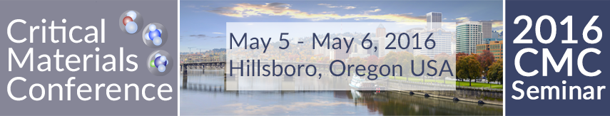
The next face-to-face meeting of CMC Fabs will take place May 3-6, 2016 in Hillsboro, Oregon. The meeting will include the annual CMC Materials Seminar held on May 5-6 that is open to the public. Sessions include a market briefing, supply chain issues and methods, the evolution of emerging materials in ALD / ALE, and the materials revolution around carbon. Speakers will be drawn from fabs, suppliers and analysts to address topics of concern and interest to the Council, and the semiconductor materials supply chain.


CMC Fabs is a unit of TECHCET CA LLC, a firm focused on Process Materials Supply Chains, Electronic Materials Technology, Materials Market Research and Consulting for the Semiconductor, Display, Solar/PV, and LED Industries. The company has been responsible for producing the SEMATECH Critical Material Reports since 2000.

Wednesday, January 6, 2016

News Flash - Volvo XC90 first car with ALD High-k/Metal Gate FinFET technology

Recently we had Audi and Samsung announcing that ALD High-k DRAM volatile memory will be used in future joint electronics in Audi cars. At CES in Las Vegas Nvidia Corp. unveiled a new, lunchbox-size super-computer for self-driving cars and said Volvo Car Group will be the new device's first customer. Volvo plans to install the device in 100 cars to be launched in 2017 as part of a large-scale trial of autonomous driving technology in Göteborg, Sweden. [Reuters]

Googling around I found what Logic is used and it seems to be 16 nm TSMC FinFET technology and then we  should have round about 10 ALD process steps or maybe even more!


Nvidia Drive PX 2 (Bild:Nvidia/Screenshot: Golem.de). Since it says 16nm and not 14nm we can assume that the CPU is fabricated by TSMC in Taiwan.


Nvidia CEO Jen-Hsun Huang Keynote speaker at CES shows the Hardware module for Drive PX 2. (Bild: Nvidia)


This is how happy Zlatan Ibrahimovic was the first time he sat in his Volvo 2015 XC90 that he picked up in Paris Auto show from Volvo boss Håkan Samuelsson. Let´s hope Zlatan get the ALD upgrade as well.


Some ASM A412 Large Batch Furnaces form inside a TSMC 300mm Fab (Photo : Copyright® Taiwan Semiconductor Manufacturing Company Limited 2010-2016, All Rights Reserved. )

Tuesday, January 5, 2016

JVSTA ALD & ALE issue is here!

JVSTA ALD & ALE issue is here - Goldig as they say in German!


Review Articles

Atomic layer deposition on polymer fibers and fabrics for multifunctional and electronic textiles

Alexandra H. Brozena, Christopher J. Oldham and Gregory N. Parsons

J. Vac. Sci. Technol. A 34, 010801 (2016); http://dx.doi.org/10.1116/1.4938104

ALD & CVD Metal Manganese Precursors from Canada


The other day we had a paper by Barry Lab on how to make your own gold ALD precursor and now here another hot topic in ALD & CVD of Metal Manganese and for sure also this paper is from Canada as well! Manganese is being evaluated by Intel, Imec and others for sub 10 nm Cu barrier in BEOL metallization. Even if those barriers are just a couple of nano meters thin it is big business since the potential in BEOL is huge if the processes were to be used for a multiple wafer passes of the BEOL Cu metallization. Recently at 20/14 nm. It will be interesting to follow if Manganese will put up a fight against Cobalt or the slugger Ruthenium for future interconnect barriers and Cu caps.

Base-Free and Bisphosphine Ligand Dialkylmanganese(II) Complexes as Precursors for Manganese Metal Deposition

Jeffrey S. Price, Preeti Chadha, and David J. H. Emslie
Organometallics, Article ASAP, DOI: 10.1021/acs.organomet.5b00907
Publication Date (Web): December 30, 2015


Graphical abstract
 

The solid-state structures and the physical, solution magnetic, solid-state magnetic, and spectroscopic (NMR and UV/vis) properties of a range of oxygen- and nitrogen-free dialkylmanganese(II) complexes are reported, and the solution reactivity of these complexes toward H2 and ZnEt2 is described. The compounds investigated are [{Mn(μ-CH2SiMe3)2}] (1), [{Mn(CH2CMe3)(μ-CH2CMe3)2}2{Mn(μ-CH2CMe3)2Mn}] (2), [Mn(CH2SiMe3)2(dmpe)] (3; dmpe = 1,2-bis(dimethylphosphino)ethane), [{Mn(CH2CMe3)2(μ-dmpe)}2] (4), [{Mn(CH2SiMe3)(μ-CH2SiMe3)}2(μ-dmpe)] (5), [{Mn(CH2CMe3)(μ-CH2CMe3)}2(μ-dmpe)] (6), [{Mn(CH2SiMe3)(μ-CH2SiMe3)}2(μ-dmpm)] (7; dmpm = bis(dimethylphosphino)methane), and [{Mn(CH2CMe3)(μ-CH2CMe3)}2(μ-dmpm)] (8). Syntheses for 14 have previously been reported, but the solid-state structures and most properties of 24 had not been described. Compounds 5 and 6, with a 1:2 dmpe/Mn ratio, were prepared by reaction of 3 and 4 with base-free 1 and 2, respectively. Compounds 7 and 8 were accessed by reaction of 1 and 2 with 0.5 equiv or more of dmpm per manganese atom. An X-ray structure of 2 revealed a tetrametallic structure with two terminal and six bridging alkyl groups. In the solid state, bisphosphine-coordinated 38 adopted three distinct structural types: (a) monometallic [LMnR2], (b) dimetallic [R2Mn(μ-L)2MnR2], and (c) dimetallic [{RMn(μ-R)}2(μ-L)] (L = dmpe, dmpm). Compound 3 exhibited particularly desirable properties for an ALD or CVD precursor, melting at 62–63 °C, subliming at 60 °C (5 mTorr), and showing negligible decomposition after 24 h at 120 °C. Comparison of variable-temperature solution and solid-state magnetic data provided insight into the solution structures of 28. Solution reactions of 1-8 with H2 yielded manganese metal, demonstrating the thermodynamic feasibility of the key reaction steps required for manganese(II) dialkyl complexes to serve, in combination with H2, as precursors for metal ALD or pulsed CVD. In contrast, the solution reactions of 18 with ZnEt2 yielded a zinc–manganese alloy with an approximate 1:1 Zn/Mn ratio.

MV Vacuum Inlet Traps for ALD Processes

Many times I get questions on how to protect the pump for your ALD reactor - last time this afternoon actually. A fist step is to put a trap before the pump. Either a cold trap (e.g. H2 cooled or N2 cooled). A water cooled trap is standard for many processes using metal halides (e.g. TiCl4) and NH3 to condense ammonium chloride. For high-k stuff like TMA and metal alkyl amides  you can use a large surface area trap like this one from MV Products. However for large amounts of precursor in large batch ALD furnaces running 24/7 you have to talk to the experts when designing a reliable abatement system - Saftey first!


NORTH BILLERICA, MA--(Marketwired - Jan 5, 2016) - MV Products has introduced a line of vacuum pump inlet traps that are designed to protect vacuum pumps used in Atomic Layer Deposition (ALD) processes in research and production environments.

MV Vacuum Inlet Traps for ALD Processes are designed to prolong vacuum pump life and reduce service intervals by removing large solids and volatile precursors from the vacuum stream. Featuring stainless steel construction and multiple plumbing options, two models are offered: the MV Multi-Trap® for production use that is capable of up to 2,500 IN3 of solids accumulation and the PosiTrap® for smaller research and development applications.

Utilizing replaceable filter elements, MV Vacuum Inlet Traps for ALD Processes can be equipped with stainless steel gauze, micron-rated polypro-pylene, activated alumina or charcoal, Sodasorb®, and other types to remove residual solvent vapor acids and particulates. The MV Multi-Trap® includes a knock-down stage and can be configured with up to six stages of filters or a single large 13" H x 14" dia. pleated high-temp. polyester filter.

MV Vacuum Inlet Traps for ALD Processes are priced depending upon size and configuration. Price quotations are available upon request.

Call for abstracts - Novel High k Application Workshop 2016, NaMLab, Dresden

In collaboration with the EU COST networking project HERALD (working group 4), NaMLab invites to the ‘Novel High-k Application Workshop’ on March 14th and 15th, 2016. New challenges offered by the application of high-k dielectric materials in micro– and nanoelectronics will be discussed by more than 80 participants from industry, research institutes and universities. The workshop was initiated as a stimulating European platform for application-oriented scientists to exchange ideas and discuss latest experimental results on MIM-capacitors, process technologies, leakage & reliability as well as characterization of high-k dielectrics integrated in silicon based micro– and nanoelectronics. In addition, new results in the field of ALD dielectrics in solar cells, transparent conduction oxides (TCOs) and atomic layer etching (ALE) will be discussed.

 A long list of speakers already confirmed their participation at the workshop. A preliminary program can be found here: http://www.namlab.com/news/events-1/novel-high-k-application-workshop


To participate in the workshop, please apply by the end of January 2016 with a ½ page abstract (oral or poster) describing the work you would like to present. Mail your abstract to ALD@namlab.com

Since the HERALD project aims to promote participation from new EU member countries, additional travel grants (up to €300 per person) are available. If you would like to apply for a travel grant, please state this in your email.

Sponsors:

Monday, January 4, 2016

The Conference Registration for ALD2016 in Dublin is now Open!


Conference Registration - 16th International Conference on Atomic Layer Deposition (ALD 2016 Ireland) incorporating Atomic Layer Etching 2016 Workshop: http://ald2016.com/event-registration/
 
Early Registration: until 31 March 2016
Standard: 1 April to 17 June 2016
Late Registration: 18 June to 18 July 2016


Welcome to the 16th Atomic Layer Deposition Conference


The 16th International Conference on Atomic Layer Deposition (ALD 2016) will be a three-day meeting dedicated to the science and technology of atomic layer controlled deposition of thin films.  In every year since 2001, the conference has been held alternately in United States, Europe and Asia, allowing fruitful exchange of ideas, know-how and practices between scientists. This year, the ALD conference will incorporate the Atomic Layer Etching 2016 Workshop, so that delegates at the two events can interact freely.  The conference will take place on 24-27 July 2016 at the Convention Centre Dublin, Ireland.

Atomic Layer Deposition (ALD) is used to fabricate ultrathin and conformal thin film structures for many semiconductor and thin film device applications. A unique attribute of ALD is that it uses sequential self-limiting surface chemistry to achieve control of film growth in the monolayer or sub-monolayer thickness regime. ALD is receiving attention for its applications in leading-edge electronic technologies, advanced microsystems, displays, energy capture and storage, solid state lighting, biotechnologies and medical technologies. Indeed ALD is particularly advantageous for any advanced technology that requires control of film structure in the nanometer or sub-nanometer scale.
As in past conferences, the meeting will be preceded by one day of tutorials. An industry trade show will be held in conjunction with the conference, to act as common ground for academia and industry to meet and discuss the future applications of ALD. Extra opportunities for collaboration will be provided through working groups of the COST Action ‘Hooking together European research in atomic layer deposition (HERALD)’.

This conference offers an excellent opportunity to learn about the most recent R&D activities in ALD science and technology from researchers around the world. We look forward to your participation.
ALD 2016 Co-Chairs:

Simon Elliott, Tyndall National Institute , Ireland Jonas Sundqvist, Division of Solid State Physics, Lund University, Sweden
Simon Elliott
Tyndall National Institute,
Ireland
Jonas Sundqvist
Division of Solid State Physics,
Lund University, Sweden

Sunday, January 3, 2016

ALD History Blog: Baltic ALD 2015, Tartu: travel notes by Riikka Puurunen

ALD History Blog: Baltic ALD 2015, Tartu: travel notes by Riikka Puurunen - The 13th International Baltic Conference on Atomic Layer Deposition, Baltic ALD 2015 was organised in Tartu, Estonia, September 28-29, 2015. Conference chairs were Prof. Jaan Aarik and Dr. Kaupo Kukli. Conference website: http://www.bald2015.ee/. Right after the conference, on September 30, 2015, there was the yearly meeting day of the HERALD COST network on ALD (http://www.european-ald.net/). I have not visited Tartu before, and it was very interesting to attend this Baltic ALD conference in the historical city of Tartu, where the first report of ALD (then, ALE) is from year 1983. ... more »

Saturday, January 2, 2016

Tokyo Electron release Triase+™ EX-II™ TiN Plus HT, a Single-Wafer Metallization System

Tokyo Electron Single Wafer SFD (Sequential Flow Deposition) has been dominating the market for e.g. TiN DRAM Capacitor electrodes for a long time. Recently (2013) it was updated to AFSD as in Advanced Sequential Flow Deposition. Tokyo Electron used to claim that they had this position because they had ClF3 chamber in-situ clean technology, but there are a number of other reasons. For those of you familiar with the TiCl4/NH3 ALD process know that there are two major issues:
  1. Growth nucleation - for thermal oxide it can be as many as 100 deposition cycles before growth starts.
  2. Low growth rate of 0.3 to 0.4 Å/cycle


SFD already addressed booth issues and with ASFD Tokyo Electron addressed lower thermal budget and improved conformality for high aspect ratio applications. Now it is very interesting to see what will happen when Tokyo Electron has released their new version of the ASFD process and the Trias Platform - The Triase+TM EX-IITM TiN* Plus HT single-wafer metallization system with HT as in High Temperauture. One reason to target high temprature is to achieve better performance (lover contact resistance) for Ti/TiN/W in for example:

1) Burried Word Lines in DRAM & coming RRAM

Since the introduction by Qimonda in 2008 (65nm DRAM) all companies uses burried tungsten word lines. 2014 Micron also presnted this technology for RRAM. Since this is a front end process there is absolutely no concern of process temperature.


Micron and Sony get together to build a 27-nm 16Gb Cu-ReRAM (IEDM 2014) 

2) High aspect ratio low resistivity electrodes and gates. 

Thinner electrode materials are needed due to geometrical constraints for scaled devices using high aspect ratio electrodes and metal gates like in DRAM and 2nd generation 3DNAND.


Samsung sub 20 nm DRAM technology presented at IEDM 2015 (Solid State Technology)

Samsung 1st generation 3DNAND investigated by Chipworks showing high aspect ratio metal gates and contacts.

Tokyo Electron Limited (TEL) announced today that it will begin accepting orders for the Triase+TM EX-IITM TiN* Plus HT single-wafer metallization system in April 2016.


Its base model, the Triase+ EX-II TiN, is a high-speed single-wafer ASFD* system with an optimized reactor chamber and unique gas injection mechanism. Since its introduction in January 2013, the Triase+ EX-II TiN has established itself as the standard for single-wafer ASFD TiN metallization systems, and has been adopted by memory and logic device manufacturers throughout the world. The Triase+ EX-II TiN Plus, an upgraded model that became available for booking in July 2015, has also been enthusiastically received in the market.
The continued scaling of semiconductor technologies has required that TiN processes in advanced device manufacturing become more detailed and diverse than ever before. TiN deposition systems must now overcome new technical challenges at highly sophisticated levels.

The EX-II TiN Plus HT, which will soon be available to order, has specialized hardware for high-temperature processes and is capable of depositing TiN film of a lower resistance and lower impurity-key technical requirements for advancing semiconductor scaling. Customers already using the Triase+ EX-II TiN or the EX-II TiN Plus can upgrade to the EX-II TiN Plus HT by modifying their existing systems, thereby reducing investment costs.

"The Triase+ EX-II TiN Plus HT is the latest generation system in the series," said Takeshi Okubo, Executive Officer and General Manager, SDBU at TEL. "It is equipped to perform high-temperature processes to satisfy new technical requirements resulting from the scaling of semiconductors, while maintaining the excellent within-wafer uniformity and step coverage achieved by the preceding EX-II TiN Plus. TEL will keep tackling difficult technology development issues to deliver high value-added products for broad-ranging thin film deposition applications."

* TiN: Titanium Nitride; ASFD: Advanced Sequential Flow Deposition, a low-temperature processing method for forming nanoscale metal films with highly-engineered properties.

NovaldMedical - an ALD Life Science Company from Finland

NovaldMedical - Here is a new interesting ALD applications company from Finland for Atomic Layer Deposition (ALD) application development to serve enhanced drug delivery, formulation engineering and industrial pharmaceutical manufacturing. [Thanks Riikka for tweeting this one!] Below is an overview of NovaldMedicals offering


Low temperature coatings

Cost-efficiency is one of the most frequent keywords in the health-care sector. In daily life, products such as instruments for diagnostics sample collection and analysis as well as for therapies,... read more →

Atomic Layer Deposition (ALD)

ALD is an industrial, surface controlled, self-limiting layer-by-layer technique for depositing thin films from gaseous phase of the precursors. The two most important advantages of ALD are excellent conformality and... read more → 

Pharmaceutical Development

The costs and risk of failure in drug discovery and development are increasing and development is becoming more challenging. Drug discovery creates new candidates for drug development. Drug development is... read more →

Medical Devices

The medical device category of products enables an extremely large variety of technical and biological needs to be fulfilled depending on the component or system involved. Proven biocompatibility and biofunctionality... read more →  


Thursday, December 31, 2015

ALD History Blog: VPHA & New Year 2016

ALD History Blog: VPHA & New Year 2016:

At the turn of the new year, it is always good to look back on the past year. Significant progress in VPHA occurred in VPHA in 2015 regarding many aspects:

- Better organization to allow the VPHA to proceed "by itself". VPHA-reading-overview-file, VPHA-reading-workflow and info@ vph-ald.com address enable the VPHA participants to find reading that is useful for the progress of the whole VPHA.
- VPHA organizational presentations were delivered at ALD Russia and Baltic ALD. The goal was to invite more people to get interested in VPHA and join it, which succeeded.... more »

Wednesday, December 30, 2015

How to make your own Gold ALD Precursor in the lab!

Yay! Now it is here the end of an interesting story 2015 from Barry Lab in Canada on making Gold ALD - all the details on how to make a gold ALD precursor! You can download the supporting information for free to the fresh article in Chemistry of Materials

Shoping List:
  • HAuCl4 x H2O (49.9 weight % Au) Strem Chemicals
  • 5 gTrimethylphosphine from Strem Chemicals diluted to 1.31 M solution in toluene
  • 4 x 25 mL bottles MeLi (1.6 M in diethyl ether) from Sigma-Aldrich
  • Anhydrous dichloromethane from Sigma-Aldrich
  • tetrahydrothiophene from Sigma-Aldrich
  • methyl iodide from Sigma-Aldrich
  • Diethyl ether purified using an Mbraun Solvent Purification System.


If you done your synthesis correct you should get a thickness curve like this (with a typical Canadian hockey stick incubation function) (figure from supporting information, Chem. Mater. DOI: 10.1021/acs.chemmater.5b04562)


Read the instructions below carefully & Happy New Year

P.S. by the way you may need one of these too - a Picosun PEALD reactor from Finland  a Picosun Picoplasma Lapin Kulta Edition.

Tuesday, December 29, 2015

CEA-Leti showcases 300mm quantum computing on silicon-on-insulator platform

Thanks Rob for Sharing this one in the FEP Group on LinkedIn as Semiconductor Today reported yesterday : Researchers in France believe they have made preliminary steps towards establishing a silicon-on-insulator (SOI) complementary metal-oxide-semiconductor (CMOS) platform for quantum information processing. Quantum information processing promises a revolution in cryptography and database searching. In particular, the superposition of quantum amplitudes enables a radical form of parallel processing for which a large number of potential super-efficient algorithms have been developed (and implemented on a relatively small scale in various model/prototype systems).

CEA-Leti and CEA-Inac have adapted a quantum dot technology originally developed for very-large-scale integration (VLSI) CMOS circuits. The dots are located beneath the gate electrode of field-effect transistors [Romain Lavieville et al, Nano Letters, vol15, p2958, 2015]. The dots can be populated with a small number of charge carriers (electrons or holes, depending on nFET or pFET structure), when the operating temperature is 0.1K.
 
What makes this extraordinary interesting is that the work is not done on some 10x10mm test coupon cluster tool but in a state of the art 300mm fab using standard leading edge CMOS equipment and some advanced lithography and patterning to produce those Si-nanowire - it is all production technology just around the corner.

Check out the beautiful ALD HKMG stack below - The HfSiON gate dielectric could actually be MOCVD since they do not explicitly state ALD in the paper. MOCVD High-k is used in production in the IBM common platform which next door neighbor in Grenoble to CEA/Leti, STMicro is member of together with Samsung, Globalfoundries and Panasonic.
 

TEM image showing the cross section of the 3.4 nm diameter CVD grown silicon nanowire (3.4 nm), the 7 nm thick SiO2 gate oxide, the 1.9 nm HfSiON, and the 5 nm ALD TiN/polysilicon gate [Figure from graphical abstract, Romain Lavieville et al, Nano Letters, vol15, p2958, 2015].

Sunday, December 27, 2015

Protecting silver cultural heritage objects with atomic layer deposited corrosion barriers [Open Acess]

Many ALD reactors out there are standing idle over the Christmas holidays and maybe this is a good opportunity to sneak into the lab and run some ALD protective coating on your silver silver objects you have at home. Here is an Open Source article from University of Maryland, E-squared Art Conservation Science and The Walters Art Museum on how to protect silver objects by Al2O3 ALD using a Beneq TFS500 reactor.

Protecting silver cultural heritage objects with atomic layer deposited corrosion barriers

Amy E. Marquardt, Eric M. Breitung, Terry Drayman-Weisser, Glenn Gates and R. J. Phaneuf


ALD coatings on silver knives: silver knives a bare, without an ALD coating, b with a 100 nm Al2O3 ALD coating deposited with a 0.5 s TMA pulse/1 s N 2 purge (fast deposition), and c 140 nm Al2O3 ALD coating deposited with a 1 s TMA pulse/4 s N 2 purge (slow deposition). (Heritage Science 2015, 3:37  doi:10.1186/s40494-015-0066-x)

Abstract:

Introduction

Silver, prized throughout history for its luster and shine, develops a black Ag 2 S tarnish layer that is aesthetically displeasing when exposed to atmospheric pollutants. Tarnishing, and subsequent polishing, leads to irreversible material loss and object damage. Currently, nitrocellulose coatings are often used to prevent silver from tarnishing, however non-uniform coatings and degradation over time limit their effectiveness. Atomic layer deposition (ALD) has been explored as a new method for creating dense, uniform, and conformal coatings on 3-dimensional (3D) objects that are more effective than nitrocellulose in preventing silver from tarnishing.

Results

To create high quality ALD coatings on 3D objects, slowing down the ALD process is critical to ensure proper precursor exposure. Non-ideal deposition of organo-oxy-metallic compounds can occur with fast deposition rates that do not allow sufficient flow around 3D objects. The coatings can be removed by dissolving the Al2O3 ALD films in aqueous NaOH. Thicker ALD films prevent defects from occurring on non-ideal surfaces and effectively prevent silver objects from tarnishing under ambient aging conditions

Conclusion

Thick ALD films, deposited with sufficiently long precursor pulse and purge times, may be effective in preventing complex, 3D non-mixed media silver cultural heritage objects from tarnishing. 
Amy, a Ph.D. candidate in the Department of Materials Science and Engineering at University of Maryland, created this video for a Thinkable competition. In it, she explains in a non-technical way how she is is creating and applying ceramic films to silver artifacts to protect them from tarnish. The virtually invisible films are applied using atomic later deposition (ALD) and are only nanometers thick. Amy's technique protects (www.youtube.com)


Thin Film System TFS 500 for ALD research and batch production (www.beneq.com)


Previous posts on Silver protection:

Feb 1, 2014 ... More information on the BENEQ nSILVER coating you can find here and below you can watch a Video on development of silver saving ...
Oct 16, 2014 ... Novel protective coatings for silv

Saturday, December 26, 2015

MOF integration routes enabled by the MOF-CVD process by Imec & Friends

2015 - The year of The MOF - Here is yet another publication on MOF that you should download and read if you have access to Nature Materials. Here scientists at Imec (Belgium), CSIRO Manufacturing Flagship (Australia), MBI, National University of Singapore and KU Leuven (Belgium) are using different paths to integrate CVD MOF deposition on to patterned structures. One path involves a conformal ZnO liner deposited on a 300 mm ASM Emerald PEALD reactor. So as I understand it Imec is actually now running MOFs in their leading edge 300 mm CMOS line, whih is pretty cool. Unless this work was done elsewhere like at the Hols Centre across the border in the Netherlands, who also have a 300mm ASM Emerald process module.

For your convenience I went through the process of acquiring a online license to publish the abstract and one picture from Nature - Bitteschön!


MOF integration routes enabled by the MOF-CVD process: lift-off patterning and coating of fragile features: a, Schematic diagram of MOF pattern deposition by MOF-CVD and subsequent lift-off of a patterned photoresist. b,c, Scanning electron microscopy images of the manufactured ZIF-8 patterns. d, Schematic diagram of the production of ZIF-8-coated polydimethylsiloxane pillars by soft lithography and MOF-CVD. e, Scanning electron microscopy image of MOF-CVD-coated PDMS pillars. f, Scanning electron microscopy image of identical PDMS pillars after conventional solution processing of ZIF-8. The MOF-CVD processing steps are indicated with a dashed line in a and d. Oxide and MOF films are represented in red and blue, respectively. Scale bars, 100μm for b, 10μm for c, 20μm for e,f, 1μm for insets. (Figure from Nature Materials doi:10.1038/nmat4509, Nature Publishing Group licence for online publishing: 3776661121061)

Chemical vapour deposition of zeolitic imidazolate framework thin films

Ivo Stassen, Mark Styles, Gianluca Grenci, Hans Van Gorp, Willem Vanderlinden, Steven De Feyter,  Paolo Falcaro, Dirk De Vos, Philippe Vereecken & Rob Ameloot
Nature Materials doi:10.1038/nmat4509

Integrating metal–organic frameworks (MOFs) in microelectronics has disruptive potential because of the unique properties of these microporous crystalline materials. Suitable film deposition methods are crucial to leverage MOFs in this field. Conventional solvent-based procedures, typically adapted from powder preparation routes, are incompatible with nanofabrication because of corrosion and contamination risks. We demonstrate a chemical vapour deposition process (MOF-CVD) that enables high-quality films of ZIF-8, a prototypical MOF material, with a uniform and controlled thickness, even on high-aspect-ratio features. Furthermore, we demonstrate how MOF-CVD enables previously inaccessible routes such as lift-off patterning and depositing MOF films on fragile features. The compatibility of MOF-CVD with existing infrastructure, both in research and production facilities, will greatly facilitate MOF integration in microelectronics. MOF-CVD is the first vapour-phase deposition method for any type of microporous crystalline network solid and marks a milestone in processing such materials.

Aussie receive Award and spends it all on an ALD trip to Boston

I once got an award and spend it all on a trip across the Baltic pond on a 2 week trip to Helsinki to learn about in-situ ALD from the Master Anti Rahtu and twice to visit two other masters in in-situ ALD Jaan Aarik and Kaupo Kulki in Tartu, Estonia. Here we have a lucky ALD-Guy from Down Under who gets to travel across the globe from Melbourne to Boston to spend 2 weeks of ALD in the Cambridge Nanotech ALD Applications Lab. This must be travel money well spent!

Please send us a picture!

As reported by Melbourne Centre for Nanofabrication: Congratulations to MCN (ANFF-VIC) Process Engineer, Dr Lachlan Hyde for nabbing a coveted Frater Award at this year's annual ANFF showcase in Brisbane. The Frater's are local/international travel awards aimed at fostering technical and professional growth of ANFF staff. Lachlan will be using his award to travel to Ultratech/Cambridge NanoTech's labs in Boston for a two week stint devoted to ALD process development.


MCN (ANFF-VIC) Process Engineer, Dr Lachlan Hyde receive Frater Award at this year's annual ANFF showcase in Brisbane. (Source MCN)

MCN are operating a Cambridge Nanotech ALD Fiji F200 & Savannah s100 ALD systems. The MCN is a world-class nanofabrication centre, combining cutting-edge technologies with the knowledge and skills of expert process engineers. The MCN represents a $50million investment in micro- nanotechnology infrastructure as a joint venture between six Victorian Universities and the CSIRO. It is located in the heart of the South-East Melbourne Innovation Precinct and is openly accessible to any researchers in academia, CSIRO or industry. The MCN is the largest and broadest capability within the Australian National Fabrication Facility (ANFF). By connecting the national research facilities in micro/nano fabrication, ANFF enables research institutions and industry clients around Australia to identify partners, collaborate and innovate. (http://nanomelbourne.com/)


Ultratech/CambridgeNanoTech provides thin film coating services of a variety of materials and they  have many ALD systems in their applications laboratory dedicated to coating services. In addition, they have invested in a variety of analytical instruments in house that are used to analyze and optimize deposited films ensure for quality and uniformity. (http://www.cambridgenanotechald.com/)


Friday, December 25, 2015

Self-assembled block copolymer template and ALD from Israel University of Technology

Here is a cool paper from from Prof. Gitti Frey and Moshe Moshonov at Technion, Israel Institute of Technology, Haifa Israel on Self-assembled block copolymer template and ALD. This is a rather hot topic for future nano patterning. They are using an ALD reactor that I did not come across until now - a MVD100E Applied MST system with an integrated oxygen plasma module to do ALD of ZnO into the organic films and self assembly of Block Copolymers.


The MVD100E Applied MST is a 200 mm tool capable of Molecular Vapor Deposition (MVD) and ALD for R&D or pilot manufacturing. It is designed for high performance, flexibility and reliability for the most demanding applications. Corporate and Academic Research Labs have called it their most versatile and reliable piece of equipment (http://www.appliedmst.com/mvd-100e/)

Here is also a video that I found on Youtube on how to operate the MVD100E tool from The Integrated Nanosystems Research Facility at The University of California, Irvine (INRF UCI).


Directing Hybrid Structures by Combining Self-Assembly of Functional Block Copolymers and Atomic Layer Deposition: A Demonstration on Hybrid Photovoltaics

Moshe Moshonov and Gitti L. Frey
Langmuir, 2015, 31 (46), pp 12762–12769 DOI: 10.1021/acs.langmuir.5b03282


The simplicity and versatility of block copolymer self-assembly offers their use as templates for nano- and meso-structured materials. However, in most cases, the material processing requires multiple steps, and the block copolymer is a sacrificial building block. Here, we combine a self-assembled block copolymer template and atomic layer deposition (ALD) of a metal oxide to generate functional hybrid films in a simple process with no etching or burning steps. This approach is demonstrated by using the crystallization-induced self-assembly of a rod–coil block copolymer, P3HT-b-PEO, and the ALD of ZnO. The block copolymer self-assembles into fibrils, ∼ 20 nm in diameter and microns long, with crystalline P3HT cores and amorphous PEO corona. The affinity of the ALD precursors to the PEO corona directs the exclusive deposition of crystalline ZnO within the PEO domains. The obtained hybrid structure possesses the properties desired for photovoltaic films: donor–acceptor continuous nanoscale interpenetrated networks. Therefore, we integrated the films into single-layer hybrid photovoltaics devices, thus demonstrating that combining self-assembly of functional block copolymers and ALD is a simple approach to direct desired complex hybrid morphologies.

Wednesday, December 23, 2015

ETH Zurich prints the tiniest inkjet color picture of the world

ETH Zurich reports: Researchers of ETH Zurich and ETH start-up company Scrona achieve a new world record! They have printed a color picture depicting clown fishes around their sea anemone home. This picture is as tiny as the cross-sectional area of a human hair.


The tiniest inkjet color picture of the world is as small as the cross-sectional area of a human hair or a single pixel of a retina display. (Photograph: Scrona/ETH Zurich)

Full story: https://www.ethz.ch/en/news-and-events/eth-news/news/2015/12/tiniest-color-picture-ever-printed.html

Dancing water molecules at the SrO on surface of ruthenates

Here is a very recent publication from TU Wien in Nature on adsorption of H2O molecules on a SrO surface of strontium ruthenate that should be very interesting for all ALD guys working with this process and material for e.g. MIM Capacitors. There is also a recent highlight of the publication in EurekAlert! http://www.eurekalert.org/pub_releases/2015-12/vuot-sph122115.php


This is a visualization of a dancing H2O molecule dissociating on the SrO crystal surface. (EurekAlert!, Credit : TU Wien)

EurekAlert! reports: "We studied strontium ruthenate - a typical perovskite material," says Ulrike Diebold. It has a crystalline structure containing oxygen, strontium and ruthenium. When the crystal is broken apart, the outermost layer consists of only strontium and oxygen atoms; the ruthenium is located underneath, surrounded by oxygen atoms.

A water molecule that lands on this surface splits into two parts: A hydrogen atom is stripped off the molecule and attaches to an oxygen atom on the crystal's surface. This process is known as dissociation. However, although they are physically separated, the pieces continue to interact through a weak "hydrogen bond".

It is this interaction that causes a strange effect: The OH group cannot move freely, and circles the hydrogen atom like a dancer spinning on a pole. Although this is the first observation of such behaviour, it was not entirely unexpected: "This effect was predicted a few years ago based on theoretical calculations, and we have finally confirmed it with our experiments" said Diebold

Adsorption of water at the SrO surface of ruthenates

Daniel Halwidl, Bernhard Stöger, Wernfried Mayr-Schmölzer, Jiri Pavelec, David Fobes, Jin Peng, Zhiqiang Mao, Gareth S. Parkinson, Michael Schmid, Florian Mittendorfer, Josef Redinger & Ulrike Diebold 
Nature Materials Published online, , doi:10.1038/nmat4512

Although perovskite oxides hold promise in applications ranging from solid oxide fuel cells to catalysts, their surface chemistry is poorly understood at the molecular level. Here we follow the formation of the first monolayer of water at the (001) surfaces of Srn+1RunO3n+1 (n = 1, 2) using low-temperature scanning tunnelling microscopy, X-ray photoelectron spectroscopy, and density functional theory. These layered perovskites cleave between neighbouring SrO planes, yielding almost ideal, rocksalt-like surfaces. An adsorbed monomer dissociates and forms a pair of hydroxide ions. The OH stemming from the original molecule stays trapped at Sr–Sr bridge positions, circling the surface OH with a measured activation energy of 187 ± 10meV. At higher coverage, dimers of dissociated water assemble into one-dimensional chains and form a percolating network where water adsorbs molecularly in the gaps. Our work shows the limitations of applying surface chemistry concepts derived for binary rocksalt oxides to perovskites.


3774700967338

Tuesday, December 22, 2015

A fresh review in Advanced Materials on ALD modelling

Here is a fresh review in Advanced Materials on ALD modelling from Simon Elliott and co-workers at Tyndall National Institute University College Cork. It contains an rather interesting part on MLD/ALD combination.

The article lists the following four major challenges for modelling ALD:
  1. Computing Precursor Volatility
  2. The Effect of Weak Interactions on Adsorption
  3. Modeling Plasma-Enhanced ALD
  4. Simulating Processes Over Long Time Scales

Modeling Mechanism and Growth Reactions for New Nanofabrication Processes by Atomic Layer Deposition

Simon D. Elliott, Gangotri Dey, Yasheng Maimaiti, Hayrensa Ablat, Ekaterina A. Filatova1 and Glen N. Fomengia
Article first published online: 21 DEC 2015
DOI: 10.1002/adma.201504043


Recent progress in the simulation of the chemistry of atomic layer deposition (ALD) is presented for technologically important materials such as alumina, silica, and copper metal. Self-limiting chemisorption of precursors onto substrates is studied using density functional theory so as to determine reaction pathways and aid process development. The main challenges for the future of ALD modeling are outlined.


Queen Elisabeth investigating The Tyndall Effect sporting a clean room hat and Class 100 stealth clean room gloves at a visit to Tyndall Institute, University College Cork in 2011.


Monday, December 21, 2015

New CNT based device from MIT that catches hard to detect molecules

MIT News Reports: Engineers at MIT have devised a new technique for trapping hard-to-detect molecules, using forests of carbon nanotubes. The team modified a simple microfluidic channel with an array of vertically aligned carbon nanotubes — rolled lattices of carbon atoms that resemble tiny tubes of chicken wire. The researchers had previously devised a method for standing carbon nanotubes on their ends, like trees in a forest. With this method, they created a three-dimensional array of permeable carbon nanotubes within a microfluidic device, through which fluid can flow. Now, in a study published this week in the Journal of Microengineering and Nanotechnology, the researchers have given the nanotube array the ability to trap certain particles. To do this, the team coated the array, layer by layer, with polymers of alternating electric charge.


A patterned and cylindrical structure made up of carbon nanotubes. (Courtesy of the researchers, MIT)


A zoomed in view of carbon nanotubes, showing individual tubes. (Courtesy of the researchers, MIT) 

Picosun is bringing ALD technology to Outer Space

Spaceworthy encapsulants from Picosun

Picosun Oy, leading supplier of highest quality Atomic Layer Deposition (ALD) thin film coating solutions for industrial manufacturing, successfully applies ALD technology to protect sensitive electronic components against harsh environmental conditions.


ALD oxide nanolaminates developed by Picosun have been proven to efficiently protect printed circuit board (PCB) components from aging effects such as corrosion and tin whisker formation. Corrosion typically occurs on the interface between the board and the component. Gaps in the solder tin covering the sharp edges of the component’s conducting pins may leave them vulnerable against environmental factors such as humidity, liquid and gaseous impurities. This is particularly detrimental in several high end applications where unfaltering component performance is required, such as in aerospace electronics. ALD forms ultra-thin, hermetic, inert, flexible, and protective film over the whole board, isolating even the most sensitive points from the ambient conditions. Due to the nanometer-scale thickness, the ALD film has negligible impact on the PCB functionality.

“Production-scale processing of PCBs requires production-optimized ALD technology. Picosun has unmatched and the most comprehensive expertise in providing large scale ALD solutions to various industries, not only to semiconductor and IC manufacturing but also for protection of 3D items – coins, watch and jewelry parts, and medical implants being just a few examples. Expanding our business to PCB encapsulation is yet another example of ALD’s penetration throughout the spectrum of today’s industrial manufacturing”, states Juhana Kostamo, Managing Director of Picosun. 

The Picosun-ESA contract is a part of an activity funded by the ESA programmes European Component Initiative Phase 4 and Strategic Initiative. Disclaimer: The views expressed herein can in no way be taken to reflect the official opinion of the European Space Agency.

Sunday, December 20, 2015

ALD is Global - Blog visitors All Time

As you can imagine ALD has a global interest and it is always existing to follow which countries that make it to the top 10 on a weekly basis.


This week we have The UK and Taiwan making it to the top 10 kicking out Sweden and The Netherlands. Above is the overall visitor statistics since the start. US is for sure still in the lead and France has taken up a new No.2 position pushing down Germany one down - Vive la France! Interestingly there was 5 visitors from Brazil today.

Here are some of the most popular posts in December - as you can see it is the leading edge stuff people enjoy reading about.


Essay on the history of ALD - Molecular Layering

As Riikka just announced - Now it is here the Essay on the history of creation and development of the molecular layering technique (ML) and later known as atomic layer deposition (ALD). We´re collecting contributions to make it an Open Access and are short of $1,000 of the total $3,000 needed - please contact either me or Riikka Puurunen if you would like to contribute!


Prof. V.B. Aleskovskii and his student S.I. Kol’tsov

From V. B. Aleskovskii's “Framework” Hypothesis to the Method of Molecular Layering/Atomic Layer Deposition

Anatolii A. Malygin, Victor E. Drozd, Anatolii A. Malkov and Vladimir M. Smirnov

Chemical Vapor Deposition, Volume 21, Issue 10-11-12, pages 216–240, December 2015,
DOI: 10.1002/cvde.201502013

Abstract: This essay is dedicated to the history of creation and development of the molecular layering technique (ML) which, in the modern community of non-Russian scientists, is commonly referred to as atomic layer deposition (ALD). Basic research in the field of chemical transformations of solid surfaces using the ML method in the light of the “framework” hypothesis proposed by V. B. Aleskovskii in 1952 is discussed. A number of questions raised by international scientists including those involved in the Virtual Project on the History of ALD (VPHA, 2013), and scientists from conferences in Helsinki (Finland, May 2014.), Kyoto (Japan, June 2014), and personal communications amongst peers are addressed. For the first time in English, this article provides information about V. B. Aleskovskii and S. I. Kol'tsov who are closely associated with development of the ML technique in the Soviet Union. This paper also informs the scientific community about research groups currently engaged in ML research in Russia and introduces the scientific school of “Chemistry of highly organized substances”, founded and supervised by V. B. Aleskovskii.
 
The authors express their deep gratitude to all the colleagues who initiated the writing of this review, particularly R. Puurunen and A. Abdulagatov. Special thanks to A. Abdulagatov for his valuable suggestions that helped strengthen the content of this article. The topic suggestions that have been sent to us by our colleagues from different countries have allowed us to more clearly define the structure and content of this article and we have tried our best to cover them all in detail. Great thanks to Puurunen Riikka (Finland), Sundqvist Jonas (Sweden), Pedersen Henrik (Sweden), Koshtyal Yury (Russia), van Ommen, J. Ruud, (the Netherlands). We would like to acknowledge the Russian science Foundation for partial financial support (contract No. 14-13-00597).

Saturday, December 19, 2015

How to ALD in Metal-Organic Framworks (MOFs) using Ultratech/CNT Savannah

Here is a fresh open source publication on a rather hot topic - using ALD in Metal-Organic Framworks (MOFs). It is really a fantastic publication giving step by step detailed instructions how to perform the materials synthesis. The researchers come from Northwestern University, Argonne National Laboratory and King Abdulaziz University. They are using ALD to deposit into the extremely well defined porous material. The ALD processing is performed in the popular Ultratech/Cambridge Nanotech Savannah reactor using a grid powder holder (see description below). Some of the researchers are involved in a startup company, NuMat Technologies, which is seeking to commercialize metal-organic frameworks.

 
Background:  MOFs are a class of crystalline materials that have a well-defined and atomically precise structures, exceptional porosities and the tunability of : 
  • particle size
  • pore size
  • surface area
  • density
  • topology
  • molecular affinity 
Beacuse of these exceptional properties MOFs are being investigated for a broad range of applications like: 
  • gas storage 
  • gas separation
  • heterogeneous catalysis
  • sensing
  • light harvesting
  • drug delivey 
Please check for all the details in the open-source publication below and real all the details:

Scalable synthesis and post-modification of a mesoporous metal-organic framework called NU-1000

Timothy C Wang,    Nicolaas A Vermeulen, In Soo Kim, Alex B F Martinson, J Fraser Stoddart, Joseph T Hupp & Omar K Farha  

Nature Protocols, 11, 149–162 (2016) doi:10.1038/nprot.2016.001

The synthesis of NU-1000, a highly robust mesoporous (containing pores >2 nm) metal-organic framework (MOF), can be conducted efficiently on a multigram scale from inexpensive starting materials. Tetrabromopyrene and (4-(ethoxycarbonyl)phenyl)boronic acid can easily be coupled to prepare the requisite organic strut with four metal-binding sites in the form of four carboxylic acids, while zirconyl chloride octahydrate is used as a precursor for the well-defined metal oxide clusters. NU-1000 has been reported as an excellent candidate for the separation of gases, and it is a versatile scaffold for heterogeneous catalysis. In particular, it is ideal for the catalytic deactivation of nerve agents, and it shows great promise as a new generic platform for a wide range of applications. Multiple post-synthetic modification protocols have been developed using NU-1000 as the parent material, making it a potentially useful scaffold for several catalytic applications. The procedure for the preparation of NU-1000 can be scaled up reliably, and it is suitable for the production of 50 g of the tetracarboxylic acid containing organic linker and 200 mg–2.5 g of NU-1000. The entire synthesis is performed without purification by column chromatography and can be completed within 10 d.


Structure of NU-1000 and developed post-synthetic modification methods on this platform. The blue, red and black spheres represent zirconium, oxygen and carbon, respectively. The perfluoro alkane SALIed into NU-1000 is represented in green, and the gold sphere shows the location of a metal cluster introduced into NU-1000 using AIM. [doi:10.1038/nprot.2016.001 Nature Publishing Group, Licence number 3772371203825]


Equipment setup for 250-mg-scale AIM modification for Al-AIM. (a,b) The metal screen constituting the power holder (a) and the reaction chamber of the ALD instrument (b). 
[doi:10.1038/nprot.2016.001 Nature Publishing Group, Licence number 3772371203825]


Friday, December 18, 2015

European researchers reach graphene production breakthrough, under project GRAFOL

Graphene-info reports: Researchers involved in the €10.6 million European research project called GRAFOL have reportedly demonstrated a cost-effective roll-to-roll production tool capable of making large sheets of graphene on an industrial scale. The tool operates at atmospheric pressure and at reduced operating temperature, and is proclaimed by the researchers "the best route to low-cost manufacture".


Graphene-enhanced perovskite PV (Graphene-info)

SAMCO Signs Distributor Contract with Swedish SiC CVD OEM

On December 1, 2015, SAMCO Inc. signed an international distributor agreement with Epiluvac AB, a Swedish manufacturer of silicon carbide (SiC) CVD systems. The agreement terms grant SAMCO exclusive distribution rights in Japan, Taiwan, Singapore, Malaysia and the Philippines.


Visit Epiluvac: http://epiluvac.com/

As a global enterprise, SAMCO is marketing its dry etching and various CVD systems in Asia, Europe and North America in addition to gaining market share within Japan. SAMCO's dry etching and plasma CVD technology serves applications involving wide band-gap semiconductor materials (e.g. RF devices, LEDs, semiconductor laser fabrication, power devices, etc.). Recently, SAMCO has placed its focus on selling production systems for next-generation GaN and SiC power devices, which are cornerstones to "green electronics" that have a large impact on energy conservation.


Epiluvac (headquartered in Lund, Sweden) is a technology company that has engaged in the development, production, and sale of SiC CVD systems used by research institutions around the world for power device applications since its establishment in 2013.


Having combined Epiluvac's SiC CVD system with its existing product lineup of plasma CVD, dry etching, and surface treatment systems, SAMCO offers a "one stop solution" for customers involved with SiC power device applications.

SAMCO from Japan launches ALD System for SiC and GaN Gate Oxides

Many reports on action in the 200mm fab and equipment market space these days. Here is another launch for Power Electronics (SiC and GaN). As reported by Semiconductor Today: SAMCO Inc of Kyoto, Japan, a supplier of plasma etch, chemical vapour deposition (CVD) and surface treatment systems to compound semiconductors device makers, has launched an atomic layer deposition (ALD) system focusing on gate oxide formation of silicon carbide (SiC) and gallium nitride (GaN) power devices.


SAMCO's new AL-1 ALD system.

SAMCO designs and manufactures dry etching systems, PECVD, and UV-ozone and plasma cleaning systems, delivering processing solutions for wide-bandgap semiconductor devices such as RF devices, LEDs, laser diodes and power devices.

SAMCO's new AL-1 ALD system deposits pinhole-free AlOxand SiO2 films, which are optimal for the gate oxide in GaN MOSFET, GaN MOS-HFET and 4H-SiC MOSFET devices. The system features precise film thickness control at the atomic-layer level (1.2Å per cycle at a deposition temperature of 350°C). The deposited AlOx film (with a breakdown voltage of 7.5MV/cm) also provides what is claimed to be excellent step coverage (with an aspect ratio of 32:1, width of 1.25μm, and depth of 40μm) with just 103nm-thick oxide films.

SAMCO says that the AL-1 is capable of depositing uniform oxides on an 8-inch wafer or three 4-inch wafers and is suitable for R&D and pilot production.

To strengthen its turn-key solutions for next-generation power device production, on 1 December SAMCO also signed a distributor agreement with Epiluvac AB of Lund, Sweden (which produces SiC CVD systems used in power device research).