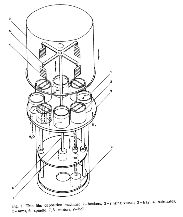
%20(1).png)
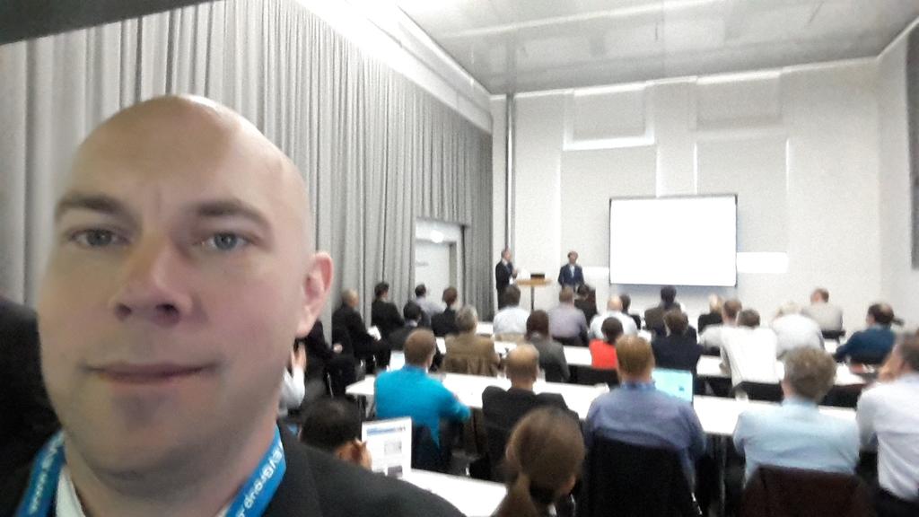
SEMICON Europa this year has turned out to be a major event for ALD and exciting nanoelectronic materials research. Here are photos taken from The ALD Day October 6th, 2015!
More details on this event you can find here : http://baldengineering.blogspot.de/2015/10/ald-ale-and-exciting-nanoelectronic.html
We are already looking forward to SEMICON Europa 2016 in Grenoble, France and to co-chair an ALD Sympoium there yet one more time!
SEMICON Europa ALD 2014, Grenoble : http://baldengineering.blogspot.de/2014/10/voila-3rd-ald-lab-dresden-symposium-at.html

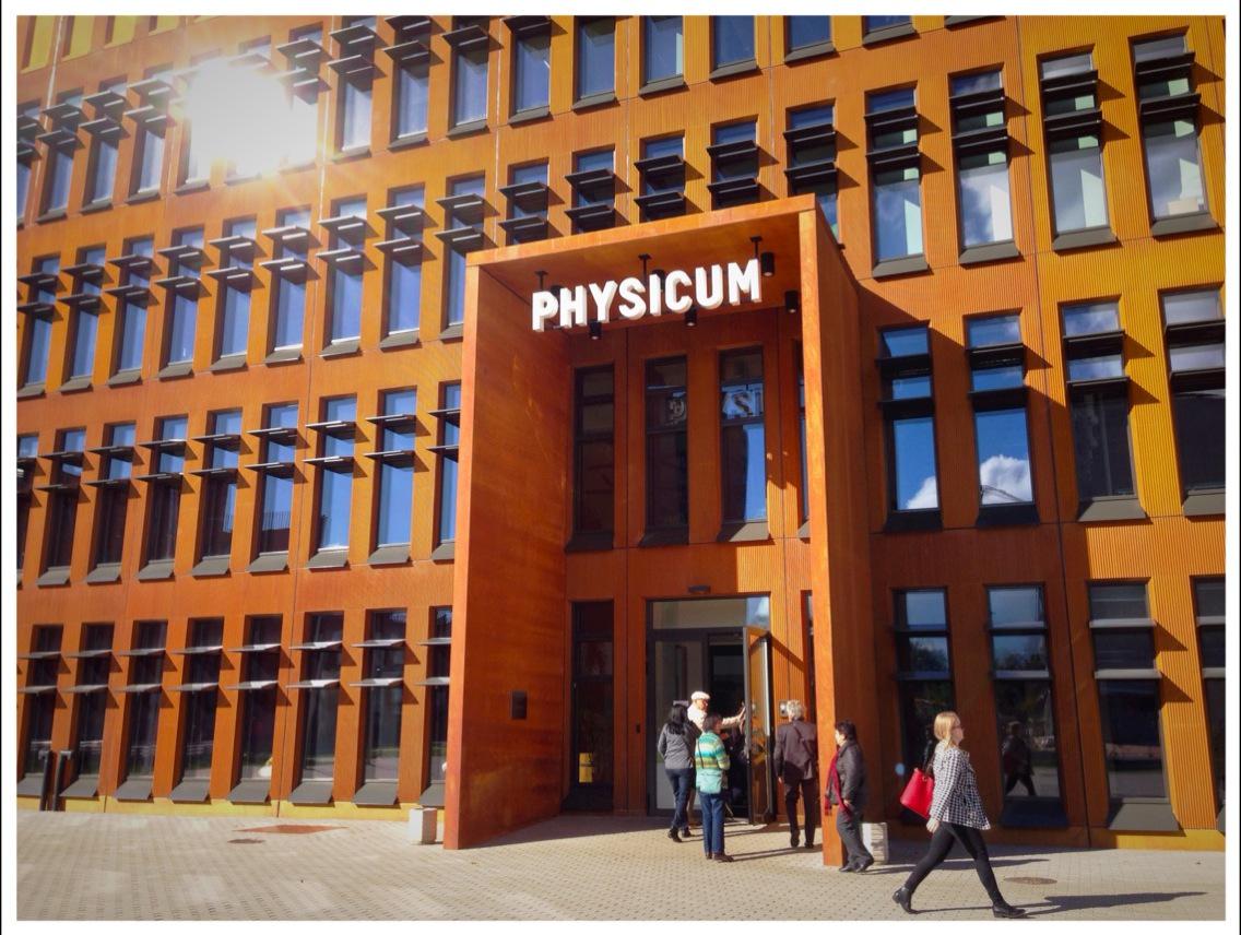
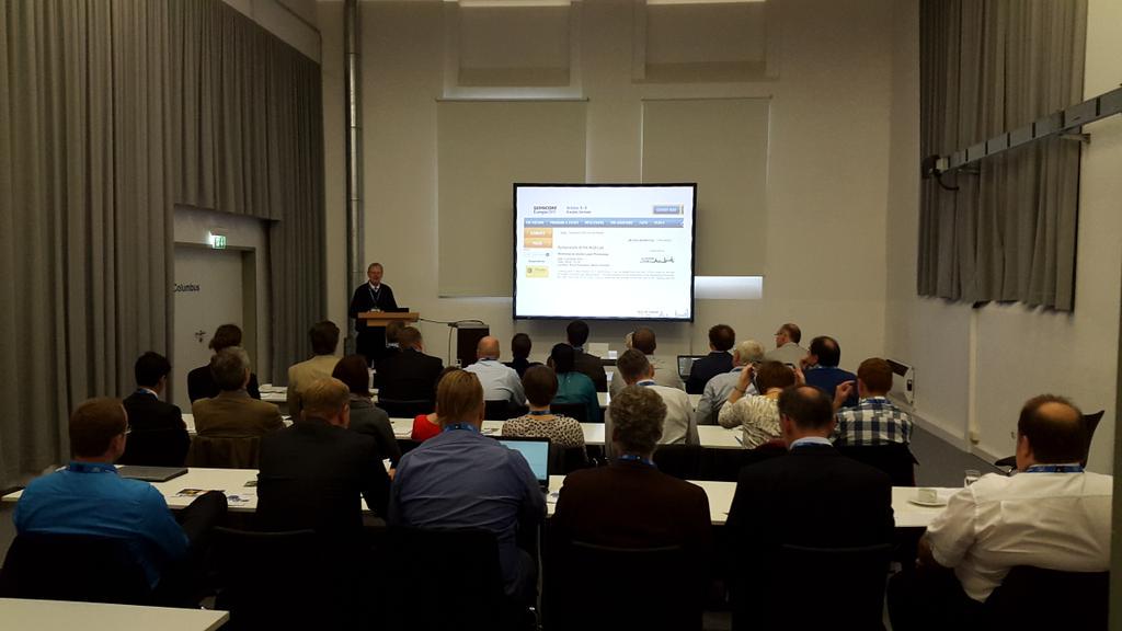
Columbus, Tuesday Oct 6, 13:45, ALD / ALE Sympoium of The ALD Lab Dresden, Messe Dreaden, Germany

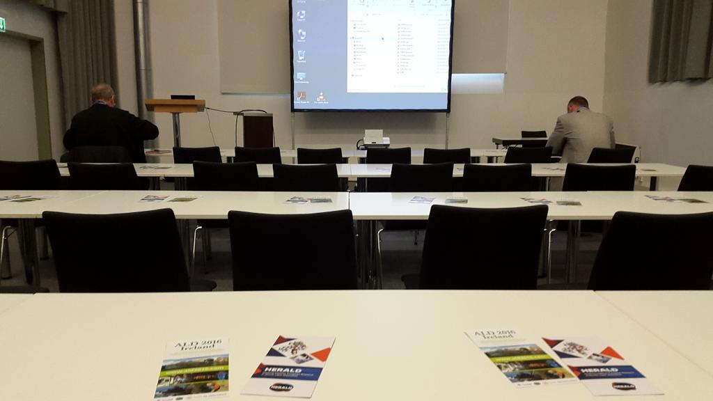
Waiting for the ALD Storm!
Welcome
Prof. Johann W. Bartha, TU Dresden
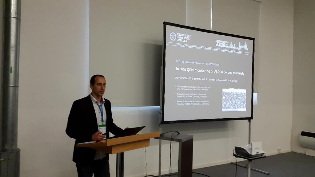
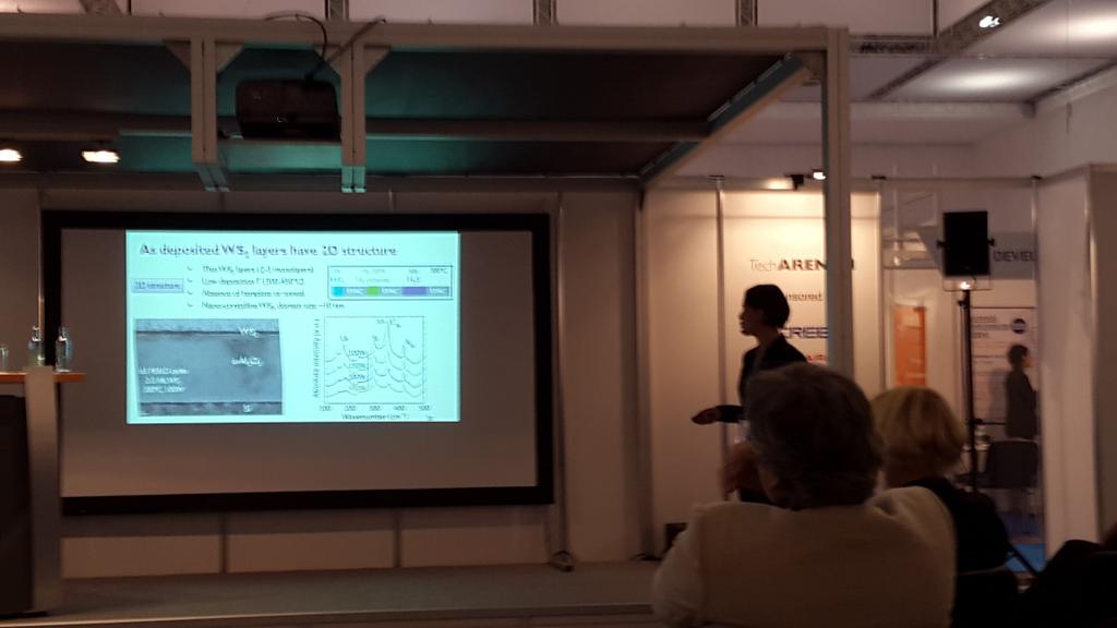
In situ monitoring of Atomic Layer Deposition in porous materials
Martin Knaut, TU Dresden
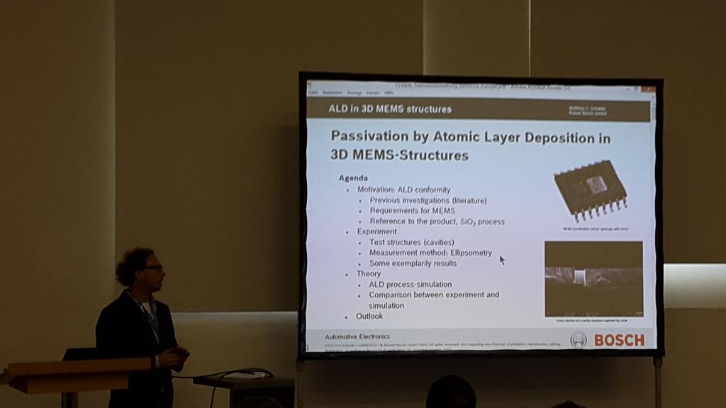
Passivation of MEMS by Atomic Layer Deposition
Matthias Schwille, Robert Bosch
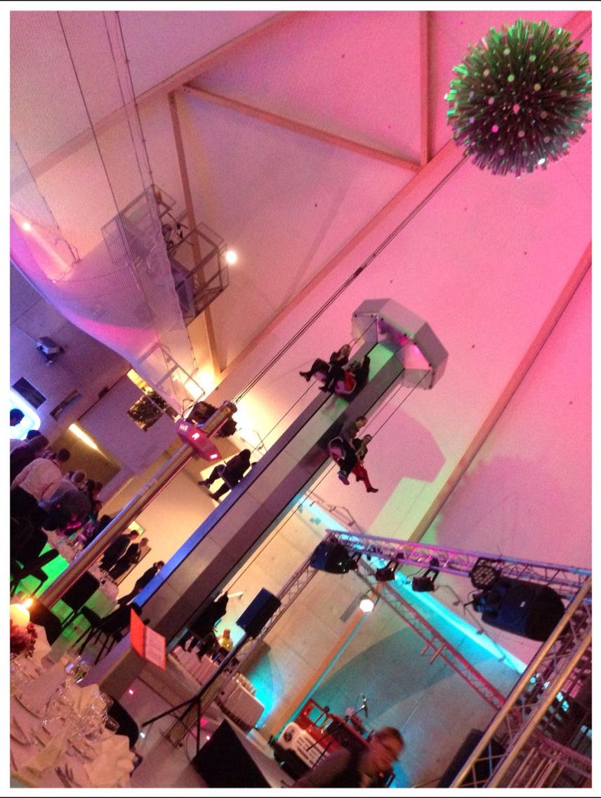
Symposium is full - please help me throw out a PVD guy
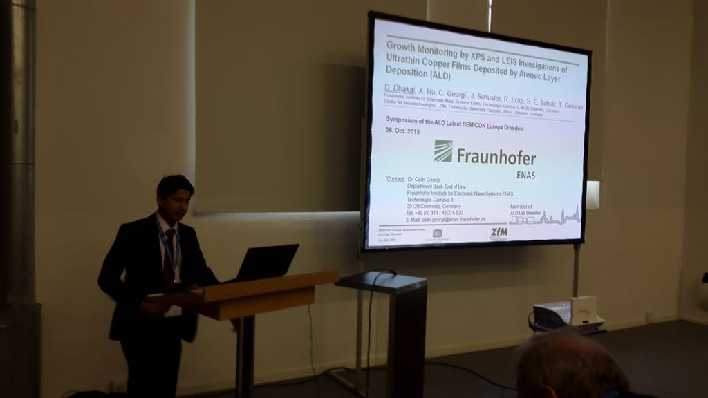
Growth Monitoring by XPS and LEIS Investigations of Ultrathin Copper Films Deposited by Atomic Layer Deposition
Dileep Dhakal, TU Chemnitz/FhG ENAS
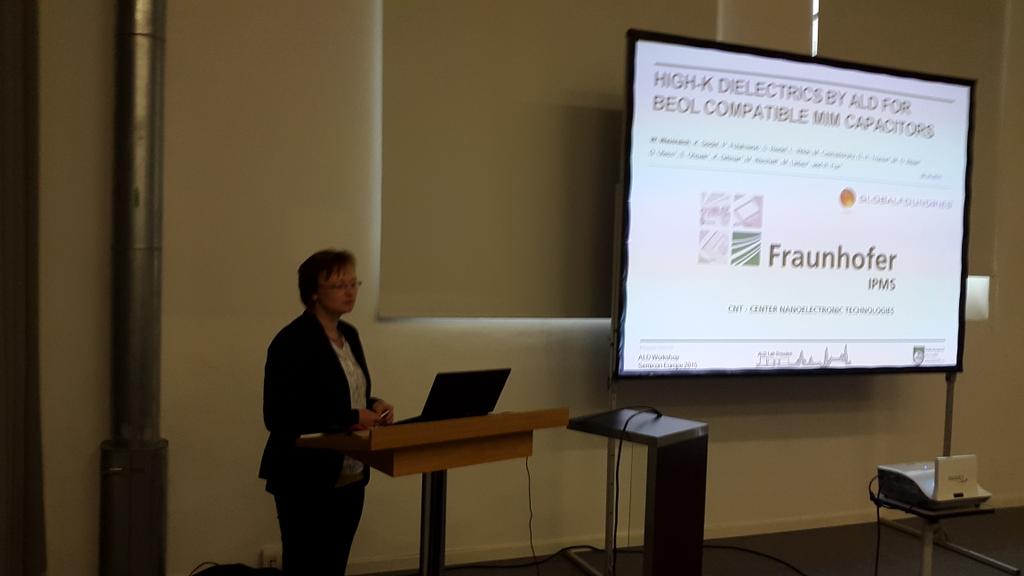
High-k dielectrics by ALD for BEOL compatible MIM
Wenke Weinreich, FhG IPMS-CNT
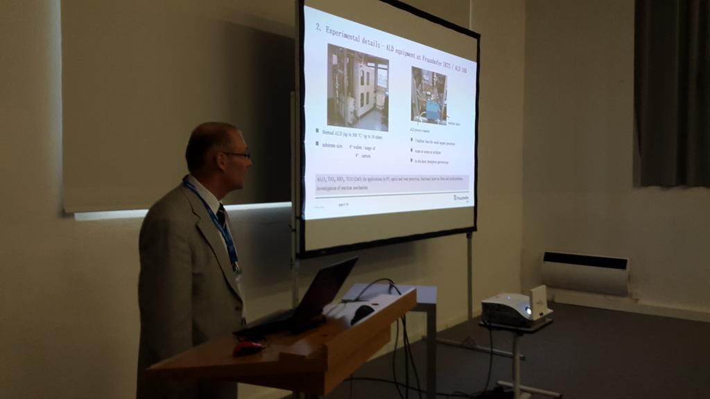
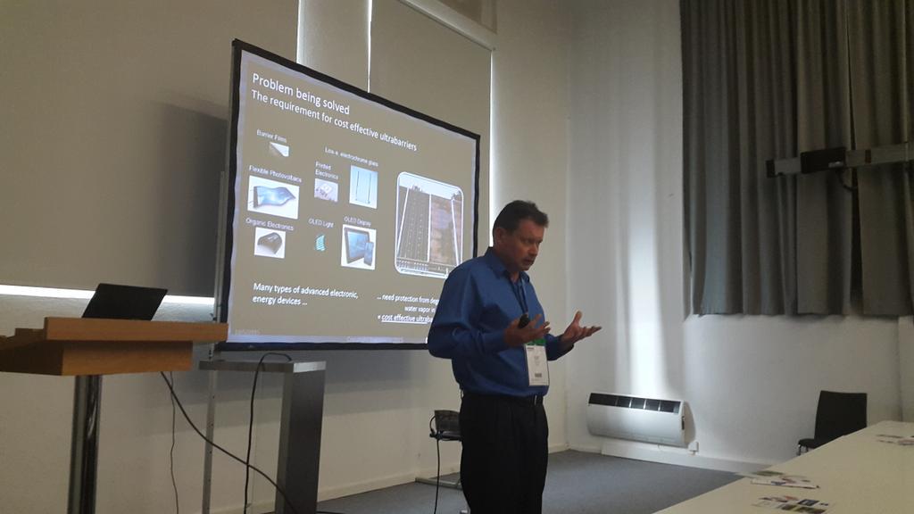
ALD coatings for applications as permeation barrier and protective layer in fiber-reinforced materials
Mario Krug, FhG IKTS
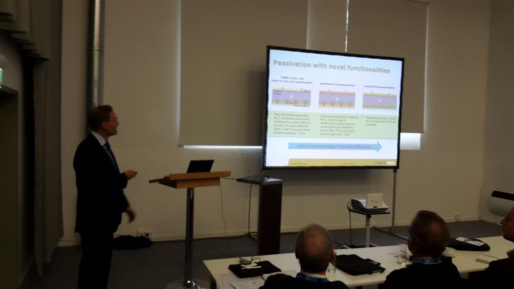
ALD for solar cell application
Ingo Dirnstorfer, NaMLab
Plasma enhanced ALD process for TiO2- and WO3- films
Alexander Strobel, FH Zwickau

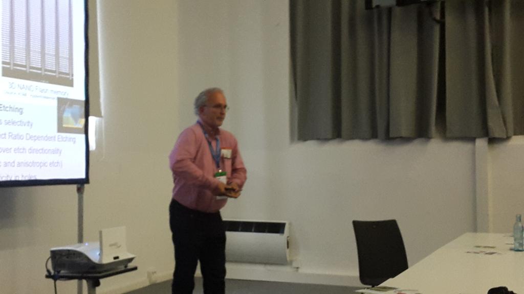
Why do we need Atomic Layer Etching
Jonas Sundqvist, Lund University/TU Dresden
Spatial Atomic Layer Deposition and Atomic Layer Etching
Prof. Fred Roozeboom, TU Eindhoven / TNO Eindhoven
Atomic Layer Etching: What Can We Learn from Atomic Layer Deposition?
Harm Knoops, Oxford Instruments/TU Eindhoven

Hardmask and side wall protection during dry etching with plasma enhanced deposition during dry etching for ALE purposes
Stephan Wege, Plasway
Industrial High Throughput Atomic Layer Deposition Equipment and Process for OLED Encapsulation
Jacques Kools, Encapsulix
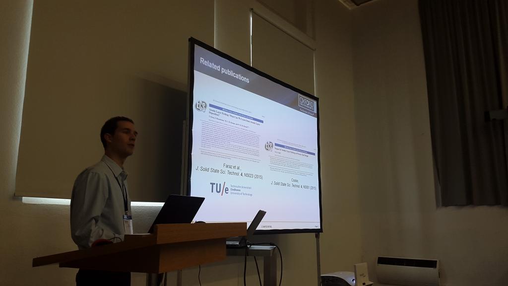
Monolayer controlled deposition of 2D transition metal dichalcogenides on large area substrates
Annelies Delabie, Imec
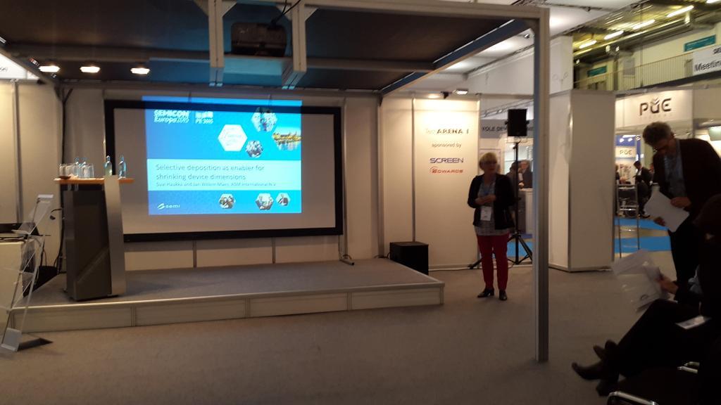
Selective Deposition as Enabler for Shrinking Device Dimensions