Header


%20(1).png)
Sunday, October 25, 2015
VPHA ALD history blog: ALD-history-evolving-file has a table of contents
VPHA ALD history blog: ALD-history-evolving-file has a table of contents: The ALD-history-evolving-file has been updated today, mainly to accommodate the Update to the Introduction. At the same time, to make it eas...
VPHA ALD history blog: VPHA status update 2015-10-21
VPHA ALD history blog: VPHA status update 2015-10-21: An email status update was sent on October 21, 2015, to VPHA co-authors and prospective co-authors. Shortened version below. If you would...
VPHA ALD history blog: Minor Wikipedia update: ALE essay added
VPHA ALD history blog: Minor Wikipedia update: ALE essay added: One of the action items in the Virtual Project on the History of ALD (VPHA) is to update the Wikipedia Atomic Layer Deposition section htt...
Self-Correcting Process for High Quality Patterning by Atomic Layer Deposition
Self-Correcting Process for High Quality Patterning by Atomic Layer Deposition
Fatemeh Sadat Minaye Hashemi, Chaiya Prasittichai, and Stacey F. Bent
ACS Nano, 2015, 9 (9), pp 8710–8717

Author Fatemah Hashemi discusses their new atomic layer deposition (ALD) approach, which combines selective etching with selective depositon. Read the related ACS Nano article at http://pubs.acs.org/doi/abs/10.1021/a...
Nanoscale patterning of materials is widely used in a variety of device applications. Area selective atomic layer deposition (ALD) has shown promise for deposition of patterned structures with subnanometer thickness control. However, the current process is limited in its ability to achieve good selectivity for thicker films formed at higher number of ALD cycles. In this report, we demonstrate a strategy for achieving selective film deposition via a self-correcting process on patterned Cu/SiO2 substrates. We employ the intrinsically selective adsorption of octadecylphosphonic acid self-assembled monolayers on Cu over SiO2 surfaces to selectively create a resist layer only on Cu. ALD is then performed on the patterns to deposit a dielectric film. A mild etchant is subsequently used to selectively remove any residual dielectric film deposited on the Cu surface while leaving the dielectric film on SiO2 unaffected. The selectivity achieved after this treatment, measured by compositional analysis, is found to be 10 times greater than for conventional area selective ALD.
Saturday, October 24, 2015
Ferroelectric HfO2 enable giant pyroelectric energy conversion and highly efficient supercapacitors
A new application for energy harvesting and storage of ferroelectric hafnium oxide has been investigated and proven by researchers at NaMLab in Dresden, RWTHA Aachen and TU Munich, Germany. One major advantage of the use of hafnium oxide over other materials is the low cost of fabrication of these films while it has been proven feasible by existing semiconductor process technology like in ALD in CMOS high-k / metal gate and high-k node dielectric for DRAM capacitors.
To summarize this investigation:

To summarize this investigation:
- Ferroelectric phase transitions in Si:HfO2 thin films yield giant pyroelectricity.
- Si:HfO2 for highly efficient supercapacitors is first reported.
- Si:HfO2 shows highest figures of merit for pyroelectric energy harvesting.
- Si:HfO2 for electrocaloric cooling and infrared sensing is first reported.
Ferroelectric phase transitions in nanoscale HfO2 films enable giant pyroelectric energy conversion and highly efficient super capacitors

Temperature- and field-induced phase transitions in ferroelectric nanoscale TiN/Si:HfO2/TiN capacitors with 3.8 to 5.6 mol% Si content are investigated for energy conversion and storage applications. Films with 5.6 mol% Si concentration exhibit an energy storage density of ~40 J/cm3 with a very high efficiency of ~80% over a wide temperature range useful for supercapacitors. Furthermore, giant pyroelectric coefficients of up to −1300 µC/(m2 K) are observed due to temperature dependent ferroelectric to paraelectric phase transitions. The broad transition region is related to the grain size distribution and adjustable by the Si content. This strong pyroelectricity yields electrothermal coupling factors k2 of up to 0.591 which are more than one order of magnitude higher than the best values ever reported. This enables pyroelectric energy harvesting with the highest harvestable energy density ever reported of 20.27 J/cm3 per Olsen cycle. Possible applications in infrared sensing are discussed. Inversely, through the electrocaloric effect an adiabatic temperature change of up to 9.5 K and the highest refrigerant capacity ever reported of 19.6 J/cm3 per cycle is achievable. This might enable energy efficient on-chip electrocaloric cooling devices. Additionally, low cost fabrication of these films is feasible by existing semiconductor process technology.
Thursday, October 22, 2015
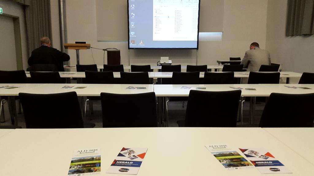
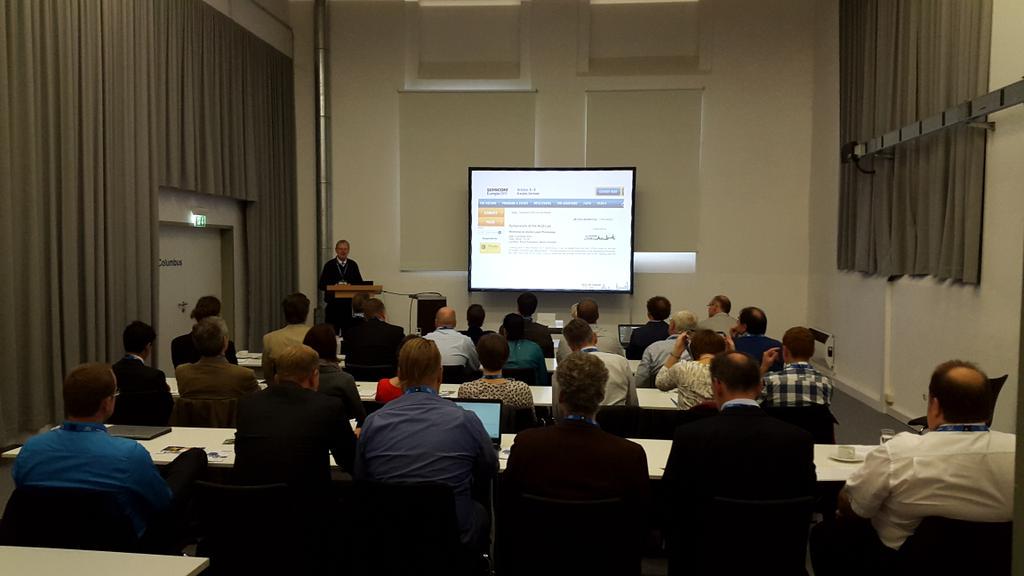
Next week : RAFALD a three-day ALD workshop November 16–18 in Grenoble, France
Atomic layer deposition, or ALD, will be the central topic at RAFALD, a three-day workshop organized from November 16–18 by several Grenoble-based ALD experts. On the docket: materials, equipment, processes, and simulation—all for an audience of professionals from industry and academia plus students enrolled in engineering programs. 50 to 100 attendees are expected.

ALD is used extensively in microelectronics and Grenoble, home to some top-notch equipment and facilities, has become one of France’s major ALD centers. The organizers are planning to build on this workshop—the first national event of its kind in France—to launch a national network dedicated to ALD. The new network could reach beyond microelectronics, attracting professionals from the energy, textile, biology, and organic electronics sectors.
- Contact: carmen.jimenez@grenoble-inp.fr
- Webite: www.rafald.org
Lundi : Tutoriels - MINATEC
- Historique et principes de base de l'ALD (F. Donsanti),
- Précurseurs (S. Danièle)
- Equipements (J. Kools)
- Appplications actuelles et émergentes (C. Vallée)
Session Posters
Mardi : Sessions scientifiques - MINATEC
- Simulations et précurseurs ALD
- Croissance, caractérisations et applications émergentes
Mercredi : Sessions scientifiques et construction du réseau - Campus Saint Martin d'Hères. Amphi OUEST Chimie
- Présentation du Labex CEMAM.
- Construction du réseau RAFALD, Réseau EU COST HERALD.
Microorganisms in the sea organize their power supply via nanowire power cables
Sorry guys, all that hard work only to find out that microorganisms in the sea organize their power supply via nanowire power cables.
Phys.org reports:


Phys.org reports:
"Electrical energy from the socket - this convenient type of power supply is apparently used by some microorganisms. Cells can meet their energy needs in the form of electricity through nanowire connections. Researchers from the Max Planck Institute for Marine Microbiology in Bremen have discovered these possibly smallest power grids in the world when examining cell aggregates of methane degrading microorganisms. They consist of two completely different cell types, which can only jointly degrade methane. Scientists have discovered wire-like connections between the cells, which are relevant in energy exchanges."
Electrical energy from
the socket - this convenient type of power supply is apparently used by
some microorganisms. Cells can meet their energy needs in the form of
electricity through nanowire connections. Researchers from the Max
Planck Institute for Marine Microbiology in Bremen have discovered these
possibly smallest power grids in the world when examining cell
aggregates of methane degrading microorganisms. They consist of two
completely different cell types, which can only jointly degrade methane.
Scientists have discovered wire-like connections between the cells,
which are relevant in energy exchanges.
Read more at: http://phys.org/news/2015-10-microorganisms-sea-power-nanowire-cables.html#jCp
Read more at: http://phys.org/news/2015-10-microorganisms-sea-power-nanowire-cables.html#jCp

Archaea (red) yield eight electrons from the oxidation of a single methane molecule. The electrons travel via the nanowires to the sulphate reducing bacteria (green). The bacteria use those electrons to convert one molecule sulphate into hydrogen sulphide. Credit: MPI f. Marine Microbiology
Electron micrograph of the nanowires shows connecting archaea and
sulphate reducing bacteria. The wires stretch out for several
micrometres, longer than a single cell. The white bar represents the
length of one micrometre. The arrows indicate the nanowires
(A=ANME-Archaeen, H=HotSeep-1 partner bacteria). Credit: MPI f.
Biophysical Chemistry
Read more at: http://phys.org/news/2015-10-microorganisms-sea-power-nanowire-cables.html#jCp
Read more at: http://phys.org/news/2015-10-microorganisms-sea-power-nanowire-cables.html#jCp
More information:
Gunter Wegener et al.
Intercellular wiring enables electron transfer between methanotrophic
archaea and bacteria, Nature (2015). DOI: 10.1038/nature15733
Read more at: http://phys.org/news/2015-10-microorganisms-sea-power-nanowire-cables.html#jCp
Read more at: http://phys.org/news/2015-10-microorganisms-sea-power-nanowire-cables.html#jCp
Electron micrograph of
the nanowires shows connecting archaea and sulphate reducing bacteria.
The wires stretch out for several micrometres, longer than a single
cell. The white bar represents the length of one micrometre. The arrows
indicate the nanowires (A=ANME-Archaeen, H=HotSeep-1 partner bacteria).
Credit: MPI f. Biophysical Chemistry
Read more at: http://phys.org/news/2015-10-microorganisms-sea-power-nanowire-cables.html#jCp
Read more at: http://phys.org/news/2015-10-microorganisms-sea-power-nanowire-cables.html#jCp
Successful industrialization of high-density 3D integrated silicon capacitors for ultra-miniaturized electronic components
Three high-tech SMEs finalize the joint EU-funded PICS project on innovative ALD materials and manufacturing equipment
Caen, Oct. 22, 2015 – Two years after the launch of the PICS project
(funded by the FP7 funding instrument dedicated to research for the
benefit of SMEs), three European SMEs, IPDiA, Picosun and SENTECH
Instruments along with CEA-Leti and Fraunhofer IPMS-CNT announce the
major technological results achieved during this program.

Two new dielectric stacks were developed and integrated into the IPDiA
3D trench capacitors by IPDiA, CEA-Leti and Fraunhofer IPMS-CNT. The
initial specifications were fulfilled and proven by electrical
measurements. A new record on capacitance density (>500nF/mm² at
3.3V) and an extended operation voltage (10V with 150nF/mm²) were
obtained, which expands IPDiA’s ability to meet current market
requirements particularly in the field of medical or aeronautics.
Qualification procedure was initiated during the project by launching
preliminary reliability studies and it will continue in the coming
months.
Read more... (369.11 kB)

Prototype of medical pills integrating temperature sensor and RF transceiver

3D trench capacitors integrated into Silicon
Publication Overview
| Title of Publication | Author(s) | Link |
|---|---|---|
| Picosun ALD enables a new generation of medical devices | Picosun | click here |
| Innovative ALD materials and tools or high densIty 3D integrated capacitors | Fraunhofer IPMS | click here |
| Presentation: NIL industrial Days (19-20 March 2015, Berlin) | Pinnow (SENTECH) | click here |
| Presentation: EuroNanoForum (10-15 June 2015, Riga) | C. Billard (CEA) | click here |
| Presentation: "Development of innovative ALD materials for high density 3D integrated capacitors” ALD Symposium, SEMICON Europe 2014 (7-9 October 2015, Grenoble) | M. Czernohorsky (Fraunhofer IPMS-CNT) | click here |
| Presentation: "Ultra-thin high density capacitors for advanced packaging solutions" 20th European Microelectronics and Packaging Conference & Exhibition (September 13-16, 2015 in Friedrichshafen, Germany) | K. Seidel (Fraunhofer IPMS-CNT) | click here |
| Presentation: "HfO2-Al2O3 nanolaminate dielectric for ultra-high integrated MIM capacitors" RAFALD workshop (November 16-18, 2015 Grenoble, France). | A. Lefevre | click here |
| PICS Poster | click here |
Wednesday, October 21, 2015
Picosun's PICOPLASMA™ technology a hit
Picosun Oy, reports continuous success for its plasma ALD technology.
Picosun’s patented* PICOPLASMA™ source system is now available on cluster integrated, SEMI S2 certified PICOSUN™ P-seriesproduction ALD modules. The remote, inductively coupled plasma with highly reactive radicals extends the selection of ALD processes and allows damage-free coating of sensitive substrates such as plastics, polymers, or metal foils. A prime example of this is the first low temperature ALD graphene deposition in a PICOSUN™ plasma ALD tool**.

Graphene depsoited by Xi'an Jiaotong University in a Picosun ALD reactor. A whole new method for the synthesis of graphene at low temperatures by means of remote plasma-enhanced atomic layer deposition (PEALD)
The PICOPLASMA™ source system is also ideal for deposition of conductive materials such as pure metals or nitrides without risk of short-circuiting or particle formation. Its optimized design enables constant breakthroughs in ALD metal processes, such as the recently reported full wafer gold deposition using Picosun’s plasma ALD technology***.

The PICOPLASMA™ source system can be mounted on existing PICOSUN™ ALD reactors or the whole PEALD system can be installed as one compact, small footprint deposition unit capable of easy implementation, quick maintenance, and low cost-of-ownership. The system can also be fully automated by integrating it into the PICOPLATFORM™ cluster tool.
“Plasma-assisted ALD processes, such as high quality noble metal or nitride layers, are becoming essential in the manufacturing of various microelectronic components. Especially in compound semiconductor device and MEMS manufacturing low processing temperatures, enabled by plasma ALD, are often crucial. The non-destructive, radical-based processing with our PICOPLASMA™ systems is enabling the future technology nodes for global semiconductor industries,” summarizes Juhana Kostamo, Managing Director of Picosun.
* Patent No. US 9,095,869; multiple patents pending
Tuesday, October 20, 2015
UPDATE Sweden will organize next EuroCVD 21 & Baltic ALD 15 conferences in 2017 in Linköping
On Monday it was decided - Sweden will organize next EuroCVD 21 conference in summer of 2017 and today it was confirmed that Baltic ALD 15 will co-organised in Linköping, Sweden.


The confirmed organizing committee Headed by Henrik Pedersen (Linköping Univ.) as conference chair and supported by Mats Boman (Uppsala Univ.), Jonas Sundqvist (Lund University/TU Dresden) and Seán Barry (Carleton Univ.)

Congratulations to Henrik Pedersen making this possible! More news will follow.
Thursday, October 15, 2015
Electrical and thermal conduction in ultra-thin freestanding ALD tungsten nanobridges
The long term master of ALD and especially W/Al2O3 laminates S.M. George and his ALD team in Boulder, Colorado have now manufactured one of the most amazing bridges that I have ever seen and it has electrical and thermal conduction as well!

Electrical and thermal conduction in ultra-thin freestanding atomic layer deposited W nanobridges
Nathan T. Eigenfeld, Jonas C. Gertsch, George D. Skidmore, Steven M. George, Victor M. BrightNanoscale, 2015, Advance Article
DOI: 10.1039/C5NR04885K, Paper
Work presented here measures and interprets the electrical and thermal
conductivities of atomic layer deposited (ALD) free-standing single film
and periodic tungsten and aluminum oxide nanobridges with thicknesses
from ∼5–20 nm and ∼3–13 nm, respectively. Electrical conductivity of the
W films is reduced by up to 99% from bulk, while thermal conductivity
is reduced by up to 91%. Results indicate phonon contribution to thermal
conductivity is dominant in these ALD films and may be substantially
reduced by the incorporation of periodicity in the ALD W/Al2O3
nanolaminates. Additionally, thin film conduction modeling demonstrates
nano-structured grain features largely dictate electron and phonon
conduction in ALD W. New fabrication methods have allowed for the
development of free-standing ultra-thin structures with layers on the
order of several nanometers utilizing ALD. While the literature contains
diverse studies of the physical properties of thin films prepared by
traditional micro-fabrication sputtering or chemical vapor deposition
techniques, there remains little data on freestanding structures
containing ALD generated materials. Specifically, knowledge of the
electrical and thermal conductivity of ALD generated materials will aid
in the future development of ultra-thin nano-devices.
RASIRC Methods for Safe and Stable Delivery of Hydrogen Peroxide Gas and Hydrazine Gas for ALD
Company presents technical sessions and exhibits at AVS Symposium
San Diego, Calif – October 14, 2015 – RASIRC will showcase a family of new technologies at the AVS 62nd International Symposium & Exhibition, October 18-23 in San Jose, California. Hydrogen peroxide gas with and without water as well as recent data on hydrazine gas for processing next generation semiconductor materials will be covered in two oral presentations and an exhibit (booth #437). The company will present “Novel Delivery of Unstable Precursors for Atomic Layer Deposition” on Monday October 19 at 4:40PM in the More Moore! II session. The company will also present “H2O2 Gas: Revolutionary new molecule for ALD” in a Technology Spotlight session.

“Next generation semiconductor devices have low thermal process budgets. Hydrogen peroxide gas and hydrazine are active molecules that allow for low temperature processing without the damage plasma can create,” said Jeffrey Spiegelman, RASIRC President and Founder. “Our Peroxidizer® and BRUTE™ product lines represent a breakthrough in stable delivery of what has been historically difficult chemicals to deliver in process.”
Hydrogen Peroxide and Hydrazine Delivery
Hydrogen peroxide in aqueous form is commonly used in semiconductor manufacturing for cleaning and surface preparation operations. However, it has limited general utility in aqueous form due to the volatility of water. In its pure state, hydrogen peroxide is highly unstable and has a propensity to decompose, forming water and oxygen. RASIRC technology uses a proprietary delivery system where 99.6% hydrogen peroxide is dissolved in non-volatile solvent.
Next generation devices have low thermal budgets and high aspect ratio structures that create new challenges for ALD grown nitride films. Hydrazine (H2NNH2) has been proposed as a thermal ALD low temperature nitride source. Hydrazine is highly flammable and its flash point decreases with reduced water content. RASIRC developed a new method and formulation for the delivery of anhydrous Hydrazine. Precursor vapor pressure is maintained at levels viable for ALD. Moreover, the addition of a proprietary solvent lowers the risk of explosion by raising the solution flash point.
Preliminary ALD data will be presented showing unique properties of these new precursors along with theoretical data on precursor delivery under variable ALD conditions.
About the Peroxidizer
The Peroxidizer is a high concentration hydrogen peroxide (H2O2) vaporizer designed specifically for the needs of next generation semiconductor processes. The Peroxidizer is the first commercial vaporizer capable of delivering concentrations greater than 5% H2O2 gas by volume from 30% H2O2 liquid source.
About BRUTE vaporizers
BRUTE Peroxide delivers anhydrous hydrogen peroxide (H2O2) for semiconductor fabrication processes such as atomic layer deposition (ALD) and atomic layer etch (ALE). BRUTE Peroxide is the only commercially available technology that can deliver up to 99.9% H2O2 gas by volume into a vacuum.
RASIRC BRUTE Hydrazine delivers water-free hydrazine (N2H4) gas into atomic layer deposition (ALD) processes. BRUTE hydrazine includes a vaporizer pre-loaded with hydrazine liquid.
AVS Symposium & Exhibition Presence
For more information about H2O2 Gas and Hydrazine delivery systems, AVS Symposium attendees are invited to visit RASIRC in booth #437. Representatives will be available to discuss technologies and test results.
Monday, October 12, 2015
New R2R ALD tool has passed factory acceptance tests at VDL ETG
According to a report on LinkedIn Flexible Electronics Group: A new R2R ALD machine operating fully at atmospheric pressure has past all factory acceptance tests this week at VDL Enabling Technologies Group (VDL ETG), The Netherlands.

The tool can deposit various atomic layers like aluminum oxide, zinc oxide, hydrogen sulfide, etc. without making use of a vacuum chamber. The adopted technology allows for extremely fast deposition rates that can even exceed by 50-100 times the deposition rates achieved in conventional vacuum-based R2R ALD tools. Built-in air bearings guarantee the scratch-free handling of the webs used as flexible substrates. The deposition can take place at temperatures as low as 80-100 degrees Celsius, which makes this R2R ALD tool extremely useful for the deposition of barriers, buffer layers, optical films, etc. in flexible electronic devices produced on plastic foils.
ALD Dielectric film with a refractive index close to air
From North Carolina State University, here is an amazing use of ALD Al2O3 and ZnO dielectric film that has optical and electrical properties similar to air, but is strong enough to be incorporated into electronic and photonic devices - making them both more efficient and more mechanically stable. Full report here and in the actual publication below as well in this supporting information file with free access : http://onlinelibrary.wiley.com/store/10.1002/adfm.201502854/asset/supinfo/adfm201502854-sup-0001-S1.pdf?v=1&s=22a54d6412037acca3bb9709f8286a3fb4877e9f
Ordered 3D Thin-Shell Nanolattice Materials with Near-Unity Refractive Indices
Xu A. Zhang, Abhijeet Bagal, Erinn C. Dandley, Junjie Zhao, Christopher J. Oldham, Bae-Ian Wu, Gregory N. Parsons and Chih-Hao Chang
Advanced Functional Materials, DOI: 10.1002/adfm.201502854


By manipulating the structure of aluminum oxide, a dielectric material, researchers were able to improve its optical and mechanical properties. The key to the film's performance is the highly-ordered spacing of the pores, which gives it a more mechanically robust structure without impairing the refractive index. You can see the structure here, on the micrometer scale.
The refractive indices of naturally occurring materials are limited, and there exists an index gap between indices of air and available solid materials. With many photonics and electronics applications, there has been considerable effort in creating artificial materials with optical and dielectric properties similar to air while simultaneously being mechanically stable to bear load. Here, a class of ordered nanolattice materials consisting of periodic thin-shell structures with near-unity refractive index and high stiffness is demonstrated. Using a combination of 3D nanolithography and atomic layer deposition, these ordered nanostructured materials have reduced optical scattering and improved mechanical stability compared to existing randomly porous materials. Using ZnO and Al2O3 as the building materials, refractive indices from 1.3 down to 1.025 are achieved. The experimental data can be accurately described by Maxwell Garnett effective media theory, which can provide a guide for index design. The demonstrated low-index, low-scattering, and high-stiffness materials can serve as high-quality optical films in multilayer photonic structures, waveguides, resonators, and ultra-low-k dielectrics.
Sunday, October 11, 2015
Wafer-scale single-domain-like graphene by defect-selective ALD of hexagonal ZnO
Korean researchers report defect-selective atomic layer deposition (ALD) for stitching grain boundaries of CVD graphene with ZnO to increase the connectivity between grains. In the present ALD process, ZnO with a hexagonal wurtzite structure was selectively grown mainly on the defect-rich grain boundaries to produce ZnO-stitched CVD graphene with well-connected grains.
Wafer-scale single-domain-like graphene by defect-selective atomic layer deposition of hexagonal ZnO
Kyung Sun Park, Sejoon Kim, Hongbum Kim, Deokhyeon Kwon, Yong-Eun Koo Lee, Sung-Wook Min, Seongil Im, Hyoung Joon Choi, Seulky Lim, Hyunjung Shin, Sang Man Koo and Myung Mo Sung

Large-area graphene films produced by means of chemical vapor deposition (CVD) are polycrystalline and thus contain numerous grain boundaries that can greatly degrade their performance and produce inhomogeneous properties. A better grain boundary engineering in CVD graphene is essential to realize the full potential of graphene in large-scale applications. Here, we report a defect-selective atomic layer deposition (ALD) for stitching grain boundaries of CVD graphene with ZnO so as to increase the connectivity between grains. In the present ALD process, ZnO with a hexagonal wurtzite structure was selectively grown mainly on the defect-rich grain boundaries to produce ZnO-stitched CVD graphene with well-connected grains. For the CVD graphene film after ZnO stitching, the inter-grain mobility is notably improved with only a little change in the free carrier density. We also demonstrate how ZnO-stitched CVD graphene can be successfully integrated into wafer-scale arrays of top-gated field-effect transistors on 4-inch Si and polymer substrates, revealing remarkable device-to-device uniformity.
UK collaboration seeks to develop new ultra-barrier materials based on graphene interlayers & roll to roll ALD
As reported by New Electronics : The Centre of Process Innovation (CPI) has announced that it has joined a UK based collaboration called ‘Gravia’, to develop the next generation of ultra-barrier materials using graphene for the production of flexible transparent plastic electronic based displays for the next generation of smartphones, tablets and wearable electronics.

The graphene market is predicted to be worth more than £800million by 2023 and could transform the manufacturing landscape in the UK.The project, including the University of Cambridge, FlexEnable and the National Physical Laboratory (NPL), expects to deliver a feasible material and process system. It builds upon existing investments by Innovate UK and the EPSRC in this area.

CPI Cleanroom
“The collaboration brings together world class supply chain expertise across the UK to bridge the gap from Graphene research to the manufacturing of commercial flexible display screens,” said James Johnstone, business development manager at CPI.
“CPI’s role in the project is to use roll-to-roll atomic layer deposition technologies to scale up, test and fabricate the ultra barrier materials.”

Beneq Roll to Roll Atomic Layer Deposition Tool - CPI offers a roll to roll atomic layer deposition (ALD) tool which is capable of handling films up to 600mm wide with thicknesses ranging from 20 – 200 µm and can produce an active coat width of 480mm.
The incorporation of graphene interlayers offers potential for flexible displays. Its gas blocking properties will enable barrier materials that are flexible, transparent, robust, and impervious to many molecules. Gravia will seek to accelerate product development, improving upon current ultra barrier performance and lifetimes by producing consistent barrier materials and processes on large area substrates by utilising specialist growth techniques. The key challenge will be to develop large-area poly-crystalline graphene films which maximise performance whilst mitigating process imperfections.
TEL signs $262 million deal with SUNY Poly to stay in Albany
As reported by Times Union : Tokyo Electron Ltd. has signed a five-year, $262.5 million extension of its research and development agreement with SUNY Polytechnic Institute in a deal that keeps the Japanese computer chip manufacturing equipment maker in Albany through 2020.

The agreement, which took effect Oct. 1 and will be officially announced Thursday, comes 12 years after the company, known in the industry as TEL, chose Albany for its first research lab outside of Japan.

The newly inked deal also is critical because TEL, which makes manufacturing equipment used in chip factories, or "fabs," is expected to play a key role in one or more manufacturing development programs in Albany involving at least $1 billion in spending by the semiconductor industry and hundreds of new jobs, the exact details of which have yet to be made public.
"New York continues to be a wonderful partner to TEL," Tetsuro Higashi, CEO of TEL said in a statement provided to the Times Union. "Through SUNY Poly, Gov. Cuomo has created one of the finest R&D centers in the world for creating next-generation chip technology, and we look forward to our continued collaboration and innovation."
Wednesday, October 7, 2015
3M licensing agreement with Lotus Applied Technology TransFlexALDTM spatial ALD
As reported today : 3M has entered into a licensing agreement with Lotus Applied Technology to access Lotus’s TransFlexALDTM spatial Atomic Layer Deposition (ALD) and barrier materials patent portfolio. TransFlexALD technology enables high-speed, low-cost deposition of single layer “ultra-barrier” coatings on rolls of polymer film using ALD. These coatings play a critical role in the encapsulation of moisture- and oxygen-sensitive electronics, such as OLED (organic light emitting device) lighting and displays, quantum dot films, photovoltaics, and flexible electronics.

“We are pleased to partner with Lotus AT and for the potential of their ALD technology to expand our ultra barrier film solutions portfolio as we integrate it with 3M’s proven technology strengths,” said John Banovetz, vice president of 3M’s Corporate Research Laboratory. “This licensing agreement and our continued product innovation will help 3M increase the performance of our ultra barrier films and offer cost-effective barrier solutions that will allow our customers to provide more competitive products in the flexible electronics markets they serve.”
3M is a leading manufacturer of flexible, transparent ultra barrier films providing encapsulation solutions for display (3M™ Flexible Transparent Barrier Film) and other sensitive electronic applications.

“We are excited to partner with 3M, a distinguished technology leader in the field of ultra barrier films,” said Eric Dickey, president of Lotus Applied Technology. “This technology offers the opportunity to radically improve the performance of single-layer barrier coatings, and 3M’s experience and expertise in this field will enable its rapid deployment in a field of applications that have been demanding higher performance at lower cost.”
(http://lotusat.com) Founded in 2007, Lotus Applied Technology was formed through a spinoff of the thin film process group within Planar Systems, Inc., a pioneer in Atomic Layer Deposition technology and manufacturing. Housed in a fully dedicated 20,000 square foot thin film processing and R&D facility in Hillsboro, Oregon, our team of technologists has been working together for over 20 years, developing innovative solutions to thin film processing challenges. Our equipment set includes a wide array of thin film deposition, lithography, and patterning equipment, including a versatile set of ALD equipment:
- Six P400 Conventional Pulse-Based Batch ALD reactors
- Roll to Roll ALD Research Scale Reactor
- TransFlex Roll to Roll ALD Pilot Scale Reactor
- Vortex Rotary Batch Reactor
Atomic Layer Processing at SEMICON Europa 2015
Here are some ALD related pictures from SEMICON Europa in Dresden. Not only ALD since this year ALE and RIE was also a hot topic in the afternoon of the ALD Lab Dresden Symposium on Tuesday (see previous post). Biggest news here is that Oxford Instruments has released new innovative hardware for ALE!

Oxford Instruments releasing new innovative hardware for ALE (Atomic Layer Etching). Harm Knoops (right) and Andreas Stamm (left)

Assuming Oxford Instrument have big success with selling ALE hardware we will definitely start seeing an increase in ALE publications in the future and maybe the upward trend of ALD will follow or the technologies will merge into one for "Atomic Layer Processing" or like some of us like to call it - ALX. This was actually the message from many of the presenter in the ALD Symposium (Prof. Bartha, Prof. Roozeboom, and Stephan Wege from Plasway), including this one from myself. The OEM market for ALX will definitely be very innovative and interesting in the years to come.

The Sentech stand a German OEM selling both Etch, PECVD and ALD / PEALD equipment together with very powerful in-situ ellipsometry metrology.

Nice to see that there is a lot of new activities in the European precursor supplier business. Here the team from EpiValence. EpiValence is focusing on working in collaboration with organisations looking for advanced chemicals and materials. Starting with research and development through to full scale up. You may also notice the close collaboration with iCAM (see their stand futher below)

A cross section of the popular Japanese ALD valves from KTZ SCT

Plasma Therm makes very technological advanced ICP RIE tools (Versaline) with lamp heated (!) chambers. Why these guys don´t make a PEALD chamber I don´t know - fast gas switching they do master for their Plasma wafer dicing process, which seems to be their cash cow.


Quick stop at the STREM to talk to Jamal Belgacem about some need for new precursor and to pick up the latest catalogues for ALD precursors

I had a nice chat with Peter Barlow at iCAM - The Bubbler Maters from Wales - about building a new flexible solid evaporator for precursor screening.
Tuesday, October 6, 2015
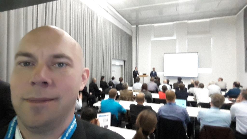
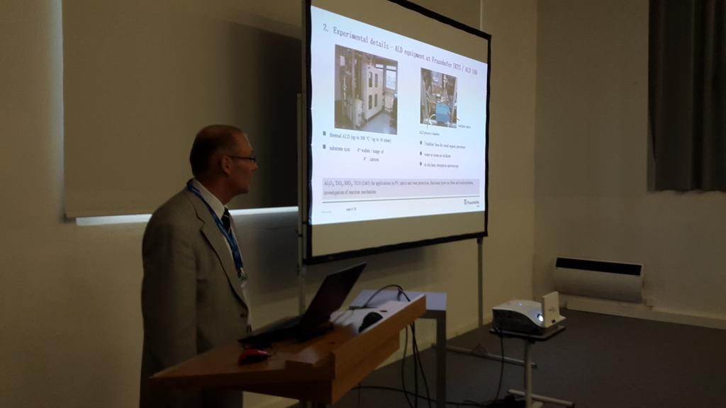
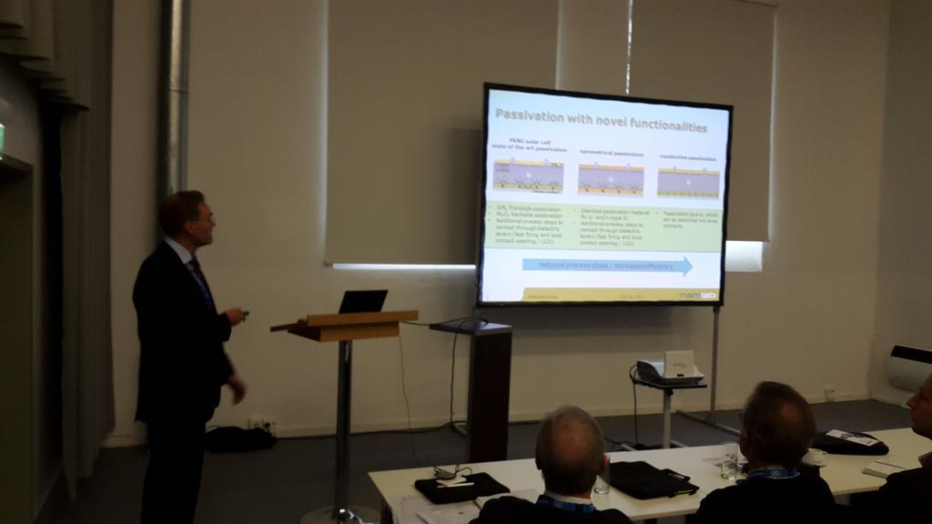
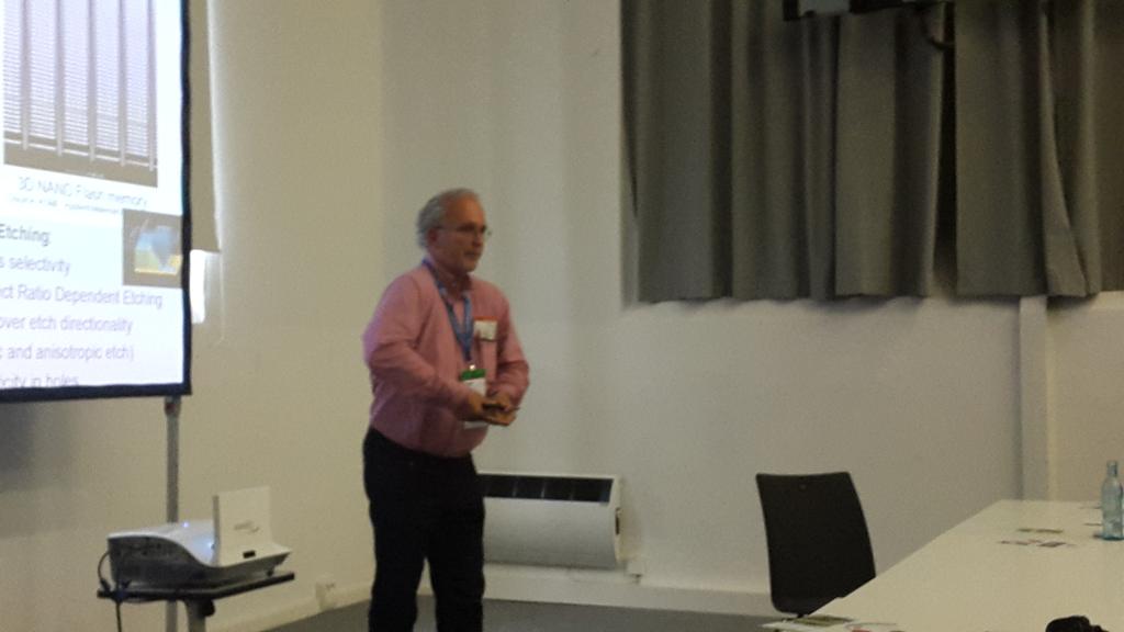
Photoshow : ALD Lab Dresden Symposium at SEMICON Europa 2015
SEMICON Europa this year has turned out to be a major event for ALD and exciting nanoelectronic materials research. Here are photos taken from The ALD Day October 6th, 2015!
More details on this event you can find here : http://baldengineering.blogspot.de/2015/10/ald-ale-and-exciting-nanoelectronic.html
We are already looking forward to SEMICON Europa 2016 in Grenoble, France and to co-chair an ALD Sympoium there yet one more time!
SEMICON Europa ALD 2014, Grenoble : http://baldengineering.blogspot.de/2014/10/voila-3rd-ald-lab-dresden-symposium-at.html

Columbus, Tuesday Oct 6, 13:45, ALD / ALE Sympoium of The ALD Lab Dresden, Messe Dreaden, Germany

Waiting for the ALD Storm!
Welcome
Prof. Johann W. Bartha, TU Dresden
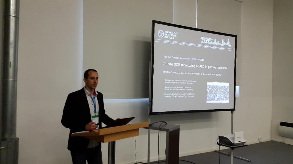
In situ monitoring of Atomic Layer Deposition in porous materials
Martin Knaut, TU Dresden
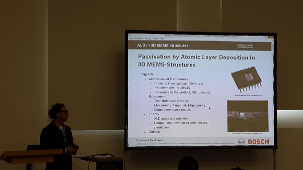
Passivation of MEMS by Atomic Layer Deposition
Matthias Schwille, Robert Bosch
Symposium is full - please help me throw out a PVD guy
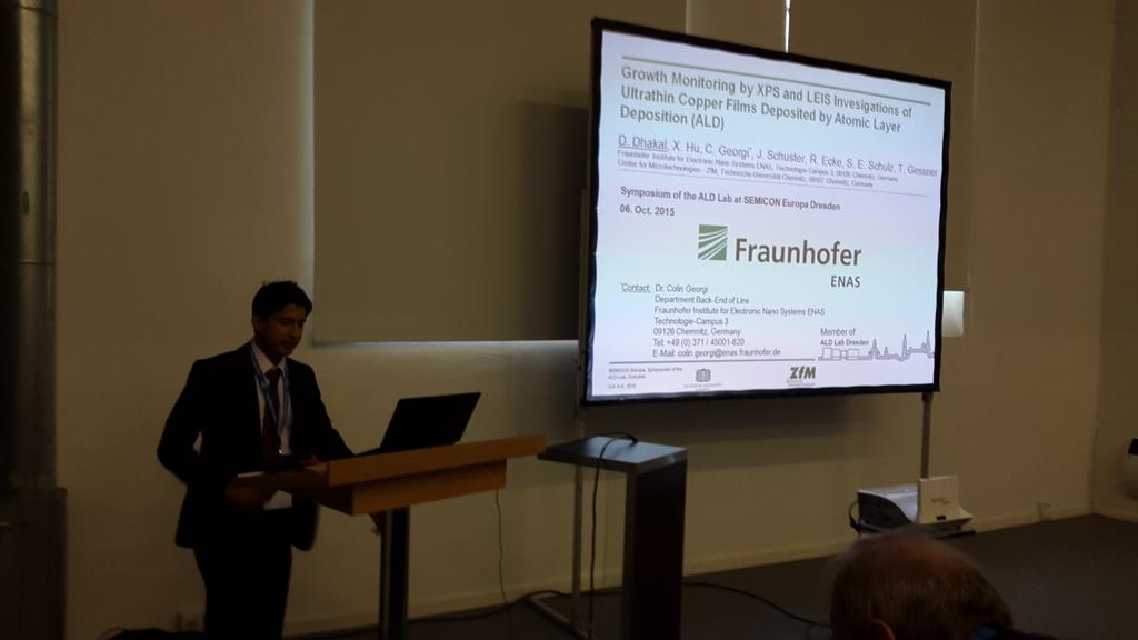
Growth Monitoring by XPS and LEIS Investigations of Ultrathin Copper Films Deposited by Atomic Layer Deposition
Dileep Dhakal, TU Chemnitz/FhG ENAS
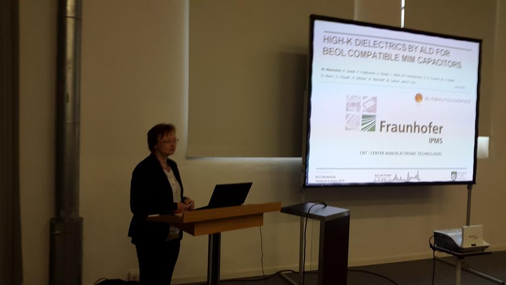
High-k dielectrics by ALD for BEOL compatible MIM
Wenke Weinreich, FhG IPMS-CNT
ALD coatings for applications as permeation barrier and protective layer in fiber-reinforced materials
Mario Krug, FhG IKTS
ALD for solar cell application
Ingo Dirnstorfer, NaMLab
Plasma enhanced ALD process for TiO2- and WO3- films
Alexander Strobel, FH Zwickau

Why do we need Atomic Layer Etching
Jonas Sundqvist, Lund University/TU Dresden
Spatial Atomic Layer Deposition and Atomic Layer Etching
Prof. Fred Roozeboom, TU Eindhoven / TNO Eindhoven
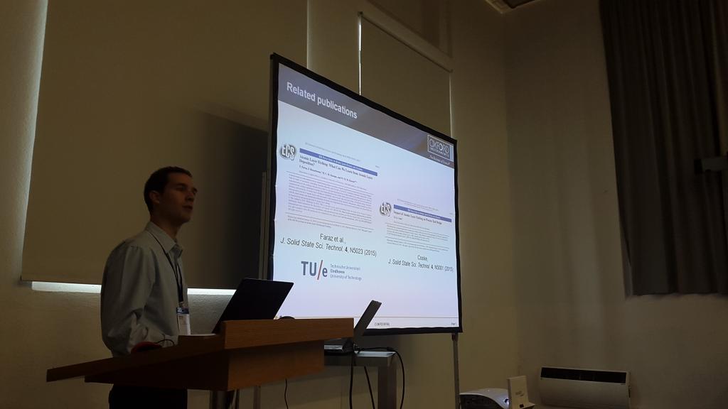
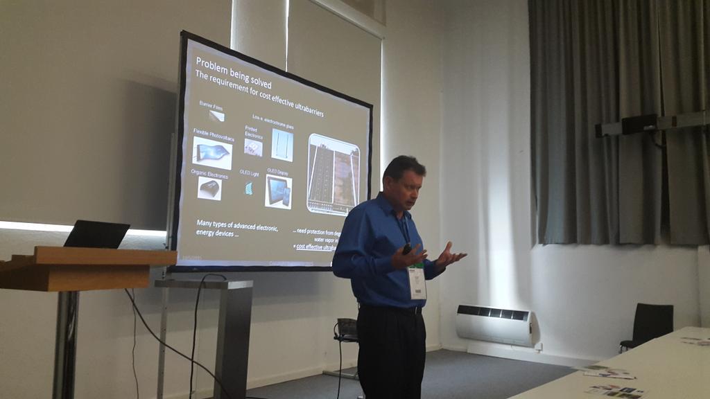
Atomic Layer Etching: What Can We Learn from Atomic Layer Deposition?
Harm Knoops, Oxford Instruments/TU Eindhoven

Hardmask and side wall protection during dry etching with plasma enhanced deposition during dry etching for ALE purposes
Stephan Wege, Plasway
Industrial High Throughput Atomic Layer Deposition Equipment and Process for OLED Encapsulation
Jacques Kools, Encapsulix
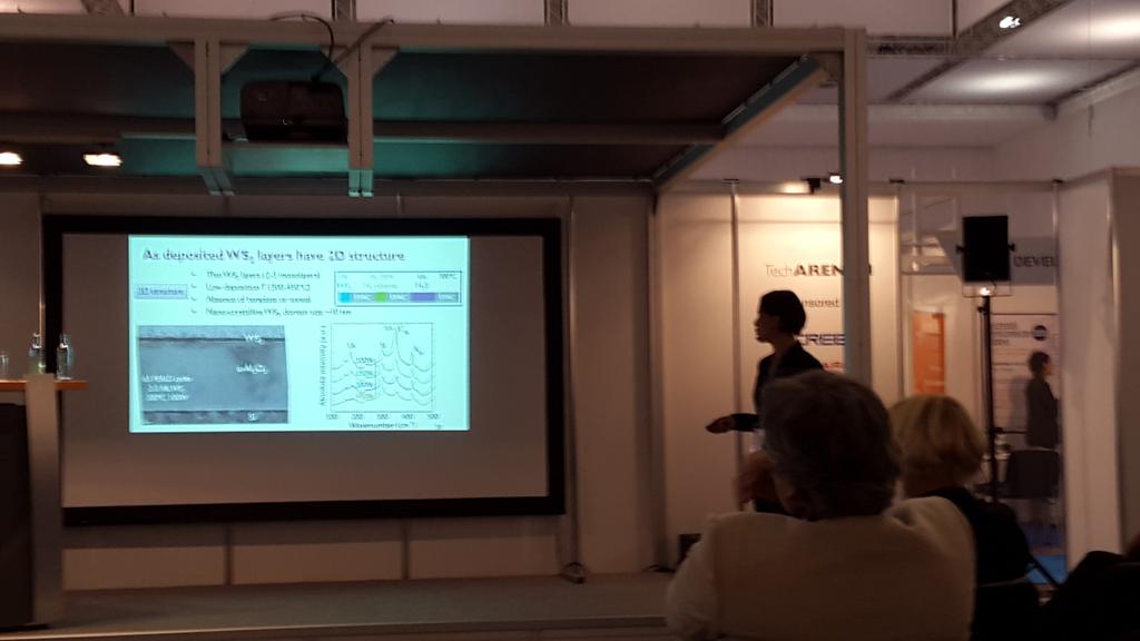
Monolayer controlled deposition of 2D transition metal dichalcogenides on large area substrates
Annelies Delabie, Imec
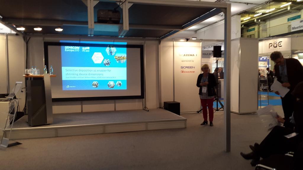
Selective Deposition as Enabler for Shrinking Device Dimensions
Suvi Haukka, Executive Scientist, ASM Microchemistry Ltd.
Subscribe to:
Posts (Atom)