AIXTRON reaches important milestone for its silicon semiconductor manufacturing technology
AIXTRON SE (FSE: AIXA; NASDAQ: AIXG), a worldwide leading
provider of advanced deposition equipment to the semiconductor industry,
announced today that a major memory manufacturer has qualified its
QXP-8300 Atomic Layer Deposition (ALD) mini-batch system (www.aixtron.com)
QXP-8300 Atomic Layer Deposition (ALD) mini-batch system suitable for
high-k oxide films in various advanced memory applications including 3D
structure devices.
“We are delighted that our customer has completed the evaluation of
our QXP-8300 ALD system for the manufacturing of the most advanced high
performance memory devices. The QXP-8300 ALD system enables the
manufacturing of advanced films with excellent electrical and device
properties. AIXTRON is looking forward to further support its customer’s
memory development plans by providing the production equipment to
address the challenges of a rapidly evolving industry,” says Bill
Bentinck, Vice President and General Manager of AIXTRON Inc., USA.
As the semiconductor memory cell size continues to be scaled down,
manufacturers need advanced technologies for the deposition of precise
layers of dielectric, metal and non-volatile memory materials. AIXTRON’s
QXP-8300 ALD system includes the patented TriJet vaporizer technology
integrated with the unique close coupled showerhead design that enables
the use of low vapor pressure precursors as needed in making higher-k
dielectrics and metal nitrides for the performance improvement.
Here are brief summary of a recent interesting article in Semiconductor Engineering by Mark LaPedus on the topic of future paths for NAND Flash Memory, which is a big market for ALD with strong competition between ASM, Lam Research and others and high aspect ration Etch Technology from Applied Materials and Lam Research. I also and added some stuff that I found elsewhere.
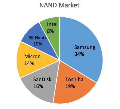
Scaling standard 2DNAND technology is coming to an end and all major NAND manufacturers are ramping 3DNAND today. The NAND market leader (34%, see below) Samsung is in the lead a shipped their first 24 layer 128 gigabit chip in 2013 and have since then introduced a 32 layer are now since last year shipping the 3rd generation 48 layer chip offering a 256 gigabit storage capacity.
Intel and Micron has joined forces in NAND (joint 22% market share) and recently started shipping a 32 layer 3DNAND chip. The other duo, SanDisk (16%) and Toshiba (19%) as well as SK Hynix (10%) are trailing Samsung with their most current 48 layer chips.
Current NAND Flash Market share - Source: Semiconductor Engineering.
3DNAND Technology - Floating Gate vs. Charge Trap Flash
Floating Gate - Micron and Intel, currently uses the floating gate
architecture
2015 Micron Presentation explaining the advantages with their 3D NAND floating gate technology shared with Intel.
Here you can read more about the Intel/Micron floating gate technology in an article by Dick James at Chipworks. I am not sure if ALD is used for the oxide and nitride layers but it is a possibility for sure due to high aspect ratio sttructures..
Charge Trap - Samsung, SK Hynix and the
SanDisk/Toshiba are all steaming up the layers using charge trap NAND.
Samsung Promo video: Samsung's 3D V-NAND flash memory is fabricated using an innovative
vertical design. Its vertical architecture stacks 32 cell layers on top
of one another, rather than trying to decrease the cells' length and
width to fit today's ever-shrinking form factors. [youtube.com]
A Look Ahead at IEDM 2015, Solid State Technology, By Dick James, Senior Technology Analyst, Chipworks
Many available cross sections of available on the internet show high-k material (Al2O3) and a metal nitride (TiN) gate being used for the to connect to the tungsten control gate. I can only assess it as ALD being used in these extreme aspect ratios.
According to a statement in the article made by Applied materials 3DNAND will make the step from 48 to 64 layers in 2016 and if it can be scaled further will be limited at some point by high aspect ration etch capability of 96 or 128 layers. However, I am a bit doubtful here that actually the technology will be limited by etch unit process engineers. As a comparison, many think that deep trench DRAM scaling was killed by high aspect ratio etch but it was not, it was rather the impossibility to scale the memory cell down from 8F2 , via 6F2 down ti a most compact 4F2 cell design. In any, case these are not extreme aspect ratios for ALD so either the etchers or the device physics will have to throw in the towel for 3DNAND momentarily. - to conclude there are two possible paths according to Mark LaPedus:
The first path:
"So going forward, NAND suppliers will simultaneously follow two parallel paths. The first path is to wait for the etch tools and other manufacturing techniques to arrive. And if they arrive on time, vendors could scale today’s 3D NAND device from 32- and 48-layers, to 64 layers, to 96 and then to 128."
The second path:
"The second path is to move towards string stacking technology. This involves stacking two or more individual devices on top each other. Each device is separated by an insulating layer. String stacking is already in the works. Recently, Micron presented a paper on a new 64-layer chip. Micron, according to multiple sources, stacked two 32-layer chips on top of each other. In theory, string stacking could involve several different combinations. For example, a vendor could stack three 32-layer chips, enabling a 96-layer device. In addition, a vendor could stack three 96-layer chips, resulting in a 288-layer product."
Recently (April 21, 2016) The North California Chapter of The American Vacuum Society (NCCAVS) Thin Film User Group organized a meeting on Advanced Memory in San Jose, California. Now all the presentations by Intel, Globalfoundries and Avalanche Technology are now available for download at the TFUG Proceedings page!
The Thin Film Users Group (TFUG) focuses on state-of-art thin-films deposition and applications for semiconductor and related fields, such as nanotechnology, renewable energy, imaging devices, design for manufacturing, and advanced memory research. It is composed of engineers and scientists from device manufactures, semiconductor equipment venders and universities. The TFUG's main activity is a bi-monthly half-day open seminar from researchers and industry technologists with technical presentations on topics of current interests.
This event was chaired by Chakku Gopalan (Intel Corporation), Co-chared by Chari Perera (Applied Materials Deposition Products Group), Paul Werbaneth (Intevac, Inc.) and Michael Oye (UCSC).
NAND Flash: Where are we, where are we going?
Pranav Kalavade, Principle Engineer at Intel, Non-volatile Memory Solutions Group, Santa Clara.
Samsung just announced that they start Mass Producing Industry’s First 10-Nanometer Class DRAM now. According to the press release (here) the key technology developments include:
improvements in proprietary cell design technology
QPT - quadruple patterning technology lithography
Ultra-thin dielectric layer deposition.
The two later ones should mean a lot of ALD business for High-k, Electrodes and dielectric spacers.
Below is a DRAM Technology Roadmap published by TechInsights last summer and here you can see that Samsung is nailing it and next we should expect announcements from SK Hynix and The Micron Camp.
Here is an earlier post form IEDM 2015 in December when Samsung revieled some details - if thoose are used here is unknown so hopefully some reverse engineering study will surface next:
Samsung to present low cost manufacturing of 20 nm DRAM and beyond at IEDM2015
Some advancement in keeping low cost manufacturing of 20 nm DRAM will be presented by Samsung at IEDM 2015. Key elements are:
avoiding EUV lithography
honeycomb structure (see figure below)
air-spacer technology
According to Solid State Technology an air-gap spacer arrangement achieves a 34% reduction in bitline capacitance for faster operation.
20nm DRAM: A New Beginning of Another Revolution (Invited),
J. Park, Y.S. Hwang, S.-W. Kim, S.Y. Han, J.S. Park, J. Kim, J. W Seo,
B.S. Kim, S.H. Shin, C.H. Cho, S.W. Nam, H.S. Hong, K.P. Lee, G.Y. Jin,
and E.S. Jung, Samsung Electronics Co.
For
the first time, 20nm DRAM has been developed and fabricated
successfully without EUV lithography using the honeycomb structure and
the air-spacer technology. These low-cost and reliable schemes are
promising key technologies for 20nm technology node and beyond.
New Critical Materials Conference's Powerful Agenda
May 5-6, Hillsboro Oregon
The Critical Materials Conference provides
a framework to catalyze the flow of "actionable" technical and supply
chain information related to critical materials.
New Additions to the Critical Materials Conference Include:
David Thompson, Ph.D., Director of Process Chemistry of Applied Materials
Agony in New Material Introductions - Minimizing and Correlating Variabilities
Suresh Ramalingam, Sr. Director, Advanced Packaging Development of Xilinx
Packaging Materials - Future Challenges
This year's conference also features speakers from
Intel, Micron, Veeco, and Air Liquide; among more than
Themes
of the Conference are centered around the needs of the Critical
Materials Council and the global IC fabrication industry. While
executive conferences typically focus on the "what" and "why" of
materials technologies, this conference will discuss "how" new materials
can be controllably, safely, and cost-effectively used in fabs. The
Conference will also include market data to validate "when" materials
will be needed. Attendees from fabs, OEMs, and materials suppliers alike
will have the opportunity to interact with the presenters and colleagues, to gain insights into best-practices of the entire supply-chain.
The Critical Materials Council for Semiconductor Fabricators,
originally established by ISMI/SEMATECH in the early 1990’s, will be
managed by TECHCET CA LLC starting January 01, 2016. Under its new name
CMC Fabs, the membership-based organization of semiconductor fab &
fabless manufacturers will continue working to identify and remediate
issues impacting the supply, availability, and accessibility of both
current and emerging semiconductor process materials. In keeping with
SEMATECH tradition, the work of the international council takes place in
a non-competitive environment for the benefit of the semi device
fabrication community. Topics addressed are identified and prioritized
by the member companies.
The organization has a new website at cmcfabs.org,
which includes an overview of the Council’s mission, news of upcoming
events and a Members Only portal for access to minutes of monthly
phone/WebEx meetings and workshop details. The site also features access
for Members to the TECHCET Critical Materials Reports and the related
quarterly updates.
The next face-to-face meeting of CMC Fabs will take place May 3-6,
2016 in Hillsboro, Oregon. The meeting will include the annual CMC
Materials Seminar held on May 5-6 that is open to the public. Sessions
include a market briefing, supply chain issues and methods, the
evolution of emerging materials in ALD / ALE, and the materials
revolution around carbon. Speakers will be drawn from fabs, suppliers
and analysts to address topics of concern and interest to the Council,
and the semiconductor materials supply chain.
CMC Fabs is a unit of TECHCET CA LLC, a firm focused on Process
Materials Supply Chains, Electronic Materials Technology, Materials
Market Research and Consulting for the Semiconductor, Display, Solar/PV,
and LED Industries. The company has been responsible for producing the
SEMATECH Critical Material Reports since 2000.
"Samsung started shipping their V-NAND last year, but that uses
charge-trap storage, in which the electrons that make up the memory bits
sit on a silicon nitride layer; the Intel/Micron device uses the
conventional floating-gate method used in planar flash, where the
electrons are stored on a polysilicon floating gate. It’ll be
interesting to see the difference!"
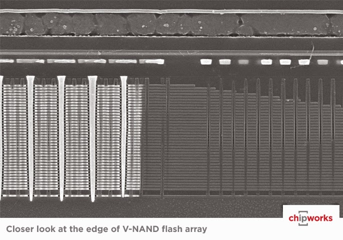
Plan-view TEM images of Samsung V-NAND flash array (Chipworks)
Looking at the rest of the stack one want to believe that also the TiN, SiO2 and SiN is deposited by ALD. However, knowing that those materials can successfully be deposited in a LPCVD or pulsed LPCVD process it can just as well be done in Large Batch furnaces from any of the companies ASM, Kokusai or Tokyo Electron. Those furnaces are for sure also capable of running the processes in a pure ALD mode though.
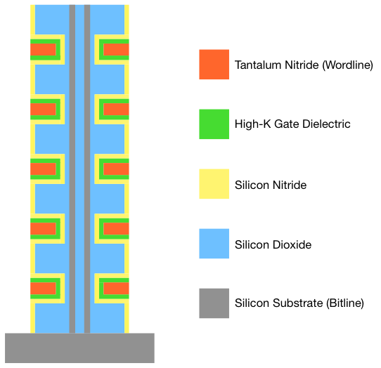
Below is a principal cross section of the first couple of cells in the Samsungs 3D NAND from
"NAND scaling in vertical dimension does not have the same
limitations as scaling in the X and Y axes do. Because the cost of a
semiconductor is still mostly determined by the die area and not by the
height, there is no need to cram cells very close to each other. As a
result, there is very little interference between the cells even in the
vertical direction. Also, the usage of high-k dielectrics means that the
control gate does not have to wrap around the charge trap. The result
is that there is a hefty barrier of silicon dioxide (which is an
insulator) between each cell, which is far more insulating than the
rather thin ONO layer in 2D NAND."
Vorsprung durch Technik - Advancement through technology - finally some ALD high-k will be introduced also for automotive electronics! As reported by Computer Business Review : "Samsung Electronics has become the first semiconductor memory supplier for Audi's Progressive SemiConductor Programme. Samsung will provide 20-nanometer LPDDR4 DRAM and 10-nanometer class eMMC (embedded multimedia card) 5.1 chips to Audi. "
Dr. Kinam Kim, President of Semiconductor Business form the Device
Solutions Division of Samsung Electronics, and Ricky Hudi, Executive
Vice President Electronic Development of Audi.
President
of Samsung Electronics Semiconductor Business Kim Ki-nam (left) signs a
contract with Executive Vice President of Audi Ricky Hudi to supply
automotive semiconductors on Nov. 23 (local time). - See more at:
http://www.businesskorea.co.kr/english/news/industry/13112-progressive-semiconductor-samsung-electronics-supply-automotive-semiconductors#sthash.a68eYl61.dpuf
"The chips are expected to be used to power Audi's future infotainment, dashboard and driver assistance applications. Audi
presently has an advanced driver assistance system which includes a
predictive efficiency assistant, adaptive cruise control, and traffic
jam assist. In September, Samsung launched the 12Gb LPDDR4 that has the largest capacity and highest speed available for a DRAM chip. It
provides 50% greater density than the existing 8GB chips used in
current smartphones, and it is also expected to help smartphones and
tablets to have up to 6GB of RAM."
LPDDR4 DRAM from Sasmsung
Audi Electronic Development
executive vice president Ricky Hudi said: "Samsung is leading memory
technology development with its high-performance, high-density DRAM and
NAND flash memory solutions based on the industry's most advanced
process technology.
From a Chipworks report abstract that can be bought here, we
can see a cross section of the stack capacitor array Samsung is using
at 26 nm (see below). For 20 nm I have not been able to find any free
available information yet
"Through the PSCP strategic partnership with
Samsung, Audi will utilize Samsung's high speed memory products to
provide the best user experience to our customers.
I am not an Audi driver but I like this picture (Picture from Audi)
"MMP technology enables atomic layer etching (ALE), providing extendibility and repeatability with atomic-scale fidelity"
Atomic-scale fidelity - Can you put it more beautiful?
LAM Research has developed a mixed-mode pulsing (MMP) technology that enables critical conductor etch for advanced memory like 3D NAND and DRAM. The technology is available for their Kiyo Product F Series chambers.
LAM Research reports: The Kiyo F Series delivers high productivity while minimizing variability for advanced memory applications. Lam's MMP technology provides advanced profile and CD control for vertical profiles with good selectivity and tuning controls for consistent etch depths. These capabilities enable higher trim rate for 3D NAND staircase etch along with excellent repeatability, which is needed for manufacturing environments. Symmetric chamber design and radial tuning provide best-in-class uniformity, which is essential for minimizing CD variability.
In addition, for new generations of advanced memory as well as logic devices, MMP technology enables atomic layer etching (ALE), providing extendibility and repeatability with atomic-scale fidelity.
By stacking memory cells vertically, NAND flash manufacturers can pack more storage capacity onto a smaller device, ease lithography requirements, and reduce manufacturing cost per bit. For multilayer 3D NAND structures, critical conductor etch processes include staircase etch and high aspect ratio (HAR) mask open for vertical channels. This mask open is crucial since it defines the CD and CD uniformity for subsequent etching of the vertical transistor channels. For staircase etch, equal-width "steps" are created at the edge of each dielectric-film pair throughout the 3D stack to form a staircase-shaped structure. Because of extensive repetition of these steps during device processing, etching at high throughput with stringent process control is vital. CD variability must be tightly managed since wordline contacts may otherwise miss landing on a step that is too narrow or uneven.
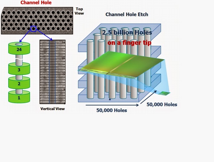
Just for visualisation for the reader of this blog, here the advance HAR etch that is required and mastered by LAM MMP Technology described in a reverse engineering cross section by Chipworks from a SAMSUNG V-NAND Flash array (published here)
LAM Research further reports with respect to DRAM : For advanced DRAM devices, depth control is a key parameter, particularly for HAR front-end-of-line silicon etch applications. Concerns include aspect ratio loading, where etch rates vary because of differences in feature dimensions, and depth loading, where different etch depths may occur due to pattern density variations.
More detailed information on mixed-mode plasma pulsing (MMP) can be found in this patent by LAM Research:
The main objective of the workshop is to bring together specialists who work in the field of dielectrics and all aspects of their application in the field of micro and nanoelectronics. The forum is intended to provide an overview of the state of the art in this significant field, and to promote a relatively informal atmosphere for the discussion of the latest research results, where contributions from students are particularly encouraged. The workshop deals with a range of issues in the field of advanced and new dielectrics, such as: growth and deposition, modelling and simulation, physical and electrical properties, reliability and dielectric applications.
Kinsale, Co Cork, Ireland, in one of the most beautiful coastal towns in Ireland.
One of the more interesting talks will be on Tuesday ;-)
09.40 “Fluorine Interface Treatments within the Gate Stack for Defect Passivation in 28nm HKMG Technology”
M. Drescher1, E. Erben2, M. Trentzsch2, C. Grass2, M. Hempel2, A. Naumann1, J. Sundqvist1, J. Schubert3, J. Szillinski3, A. Schäfer3, S. Mantl3
For all of you working on emerging memory technologies such as ReRAM, FeRAM, PCM, MRAM etc. this classification scheme in the latest ITRS roadmap should be very useful. Please check out the ERD - Emerging Research Devices Chapter.
"Figure ERD3 [inserted below] provides a simple visual method of categorizing memory technologies. At the highest level, memory technologies are separated by the ability to retain data without power. Nonvolatile memory offers essential use advantages, and the degree to which non-volatility exists is measured in terms of the length of time that data can be expected to be retained. Volatile memories also have a characteristic retention time that can vary from milliseconds to (for practical purposes) the length of time that power remains on. Nonvolatile memory technologies are further categorized by their maturity. Flash memory is considered the baseline nonvolatile memory because it is highly mature, well optimized, and has a significant commercial presence. Flash memory is the benchmark against which prototypical and emerging nonvolatile memory technologies are measured. Prototypical memory technologies are at a point of maturity where they are commercially available (generally for niche applications), and have a large scientific, technological, and systematic knowledge base available in the literature. These prototypical technologies are covered in Table ERD2 and in the PIDS Chapter. The focus of this section is Emerging Memory Technologies. These are the least mature memory technologies in Fig. ERD4, but have been shown to offer significant potential benefits if various scientific and technological hurdles can be overcome. This section provides an overview of these emerging technologies, their potential benefits, and the key research challenges that will allow them to become viable commercial technologies."
Figure ERD3, from the ERD Chapter 2013 - Emerging memory taxonomy (ITRS 2013, Chapter ERD)
If you continue to read from page 8 on you will find a short description of all emerging memory technologies that are being considered by he ITRS. If you´re saturated on resistive technologies you can fast forward to page 12 and read about the new contender FeFET :-)
Toshiba Corporation announced that it has developed the world's first 15-nanometer (nm) process technology, which will apply to 2-bit-per-cell 128-gigabit (16 gigabytes) NAND flash memories. Mass production with the new technology will start at the end of April at Fab 5 Yokkaichi Operations, Toshiba's NAND flash fabrication facility (fab), replacing second generation 19 nm process technology, Toshiba's previous flagship process. The second stage of Fab 5 is currently under construction, and the new technology will also be deployed there.
"In-keeping with semiconductor industry fast-track construction techniques and schedules, Toshiba and manufacturing partner, SanDisk have officially opened their third 300mm wafer NAND flash fabrication facility at Toshiba's Yokkaichi Operations in Mie Prefecture, Japan, dubbed Fab 5." (Fabtech)
If you want to take a visit Google Street View offers excellent view from the Toshiba site in Yokkaichi. Just tune in here in this intersection take a right turn and enjoy the drive : Toshiba Fab 5.
Screendump from Google Street View just upfront of Toshiba Fab 5 in Yokkaichi.
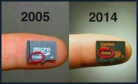
Recently this picture below was published on LinkeIn (I seen it posted by Yangyin Chen
陈杨胤, researcher at imec) and other social media and has been shared a great deal. Naturally there has been comments and questions if it will go on on heading for 128 terabit NAND flash memory 2025 or so.
To get a glimpse into how this scaling has been possible I checked out the Samsung information on V-NAND as they call their 3D-NAND technology. According to the information available on Samsungs web they have set the foundation for more advanced products including 512 gigabit (Gb) and one terabit (Tb) NAND flash memory, which we expect to develop within the next few years. structure. So single digit terabit should not be a problem. What about 128 TB? I don´t know, but I assume we will need that integrated into a Google lens to record our exiting lives in 3D-HD feeding real time in to Facebook accounts pretty soon :-)
Samsung’s new V-NAND offers a 128 gigabit (Gb) density in a single chip, utilizing the company’s proprietary vertical cell structure based on 3D Charge Trap Flash (CTF) technology and vertical interconnect process technology to link the 3D cell array. By applying both of these technologies, Samsung’s 3D V-NAND is able to provide over twice the scaling of 20nm-class planar NAND flash.By making this CTF layer three-dimensional, the reliability and speed of the NAND memory have improved sharply. The new 3D V-NAND shows not only an increase of a minimum of 2X to a maximum 10X higher reliability, but also twice the write performance over conventional 10nm-class floating gate NAND flash memory. [Far East Gizmos]
"An industry first, it represents a breakthrough in overcoming the density limit currently facing the planar NAND architecture and floating gates used in conventional flash memory, as well as yielding speed and endurance"
Check out the promo video from Samsungs YouTube channel below.


%20(1).png)