In order for IDMs and Foundries to follow Moore’s Law, semiconductor engineers have been forced to continuously shrink semiconductor device dimensions, so that some barrier layers are as thin as 3 atoms. Semiconductor processes affected by shrinkage include atomic layer deposition (ALD), annealing, wafer cleaning, thermal oxidation, thin film growth, etching, and interface layer passivation. Present materials used in semiconductors can breakdown at this atomic scale and must be replaced by new materials to meet low power consumption, high performance and low cost targets. These new replacement materials come with their own set of process challenges.
Atomic Layer Depostion
ALD has been
used in high-volume semiconductor manufacturing since 2004 [1] and according to Chuck
del Prado, CEO of ASMi, one of the world-leading companies in the field [2]:
“ALD is now firmly established as a key enabling technology. Today, ALD has become a critical technology for the manufacture of virtually all leading-edge semiconductor devices. The leading customers in our industry have already ramped several device generations based on our ALD equipment – for high-k metal gate applications in logic and foundry and for multiple patterning applications in the memory sector.”
The 3D challenge in high aspect
ratio structures
The new atomically ultrathin films are more sensitive to environmental conditions than thicker structures from past design nodes. Precise cleaning and preparation is required to prevent atoms from straying into other layers. Complicating the process is that these layers are no longer planar, but are three dimensional shapes with very high aspect ratios approaching 150:1 for DRAM memory cell capacitors and 3DNAND flash memory charge trap devices, creating inverted skyscrapers on an atomic layer.
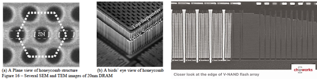
Samsung presented a low cost manufacturing of 20 nm DRAM and beyond at IEDM2015 using honeycomb structure narrow gap air-spacer technology (left). For visualisation, here (right) the advanced High Aspect Ratio etch and ALD that is required for 3DNAND flash memory manufacturing in a reverse engineering cross section by Chipworks from a SAMSUNG V-NAND Flash array.
Processing at the bottom of these extremely deep structures is nearly impossible. There are two main challenges:
- Chemicals must be stable enough to reach the bottom, but reactive enough to be effective when they contact the bottom target site.
- Low temperatures are needed to prevent migration of atoms in and out of the layers, so the chemicals must be active at low temperatures.
Chemicals used today for thin film oxidation do not meet these manufacturing challenges. This has forced R&D engineers to look for alternatives. The range of oxidants in use today include water, ozone and O
2 plasma. Yet, in one way or another, all of these oxidants are deficient for fabrication of these new device structures under atomic level constraints. To address these challenges, RASIRC has developed a new technology that enables the common liquid oxidant, hydrogen peroxide, to be converted into a controlled and repeatable oxidant gas. This new product is called the Peroxidizer®.
Hydrogen Peroxide Gas (HPG)
RASIRC specializes in products that generate and deliver gas to fabrication processes. Each unit is a dynamic gas plant in a box—converting common liquid chemistries into safe and reliable process gas on demand.. First to generate ultra-high purity (UHP) steam from de-ionized water, RASIRC technology can now also deliver hydrogen peroxide gas in controlled, repeatable concentrations.
Hydrogen Peroxide Gas (HPG) is a powerful and versatile oxidant for processing new materials and 3D structures. HPG is now available in stable, high concentration and offers significant benefits to ALD, annealing and cleaning applications. The Peroxidizer is an order of magintude improvement over its predecessor and overcomes the limits of pre‐humidification and high concentration H
2O
2 liquid supply by concentrating liquid inside the vaporizer. It handles gas flows of 5 to 30 slm in vacuum or atmospheric conditions. It delivers H
2O
2 concentrations from 12,500 to 50,000 ppm, which equates to 1.25 to 5% gas by volume. The Peroxidizer delivers a 4:1 water to Peroxide ratio. This is not possible with other high temperature vaporization methods due to H
2O
2 decomposition.
The membrane used in the vaporizer preferentially vaporizes H
2O
2 relative to water. This allows the concentration to stay below 75% and 90°C in the vaporizer while being able to generate 50,000 ppm. The fab only needs to supply 30% w/w, which is already in use throughout most facilities.
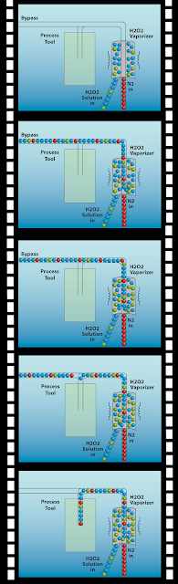
The above
frames illustrate the Peroxidizer concentration process. At top, vaporizer is filled
with 30% w/w H2O2. As move to the bottom, carrier gas
passes through vaporizer solution and water vaporizes preferentially. Last
frame shows that solution has reached mass balance and stable, high
concentration H2O2 can be sent to process.
Hydrogen peroxide is a hazardous chemical and must be handled properly to prevent exposure of operators to unsafe chemical conditions. With proper design, installation, and operator training, hydrogen peroxide can be a viable alternative to other oxidants. The Peroxidizer includes a range of safety features focused on temperature, concentration, pressure, liquid and gas leak detection, venting and liquid handling.
H
2O
2 is auto‐refill capable. If a continuous supply of 30% H
2O
2 liquid is available, the Peroxidizer can run 24/7. For R&D, the Peroxidizer can be manually refilled with an internal source container to run 4 to 24 hours depending on flow rate.
- Primary interlock loop will shutoff power when any of a number of safety conditions occur.
- Temperature safeties include redundant thermal interlocks with thermal switches for heaters.
- H2O2 liquid and headspace temperatures are interlocked into the safety control loop.
- Concentration safety features include level sensors for overfill and low liquid conditions. If liquid level is too low, an alarm is displayed and carrier gas turned off to prevent further liquid concentration.
- Pressure safety features include direct pressure monitoring, pressure relief, and direct vent lines to channel high pressure vapor directly to scrubbed exhaust in case of overpressure conditions.
- Leak safety features include a flood sensor to detect liquid leaks.
- The system is ducted for exhaust ventilation to prevent HPG exposure in case of H2O2 liquid or gas leak. A ventilation pressure switch will trigger the interlock loop if ventilation is not adequate. A ppm HPG monitor is recommended in the exhaust ducting.
- The drain line has a float switch to monitor for drain back up.
- An optional condenser is available to condense HPG and water vapor before it goes to vent. Alternatively, scrubbers can be used to convert HPG directly to oxygen and water.
To learn much more about the operating principles and process demonstration results from the HPG technology you can download a paper here: „Hydrogen Peroxide Gas Delivery for Atomic Layer Deposition, Annealing, and Surface Cleaning in Semiconductor Processing“, By Jeffrey Spiegelman, Russ Holmes and Zohreh Shamsi [
Link]
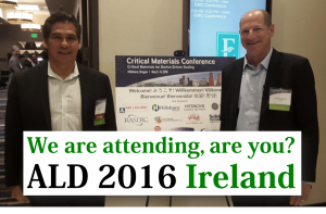
Dan Alvarez, CTO of RASIRC, will be presenting a poster entitled „Hydrogen peroxide gas for improved nucleation and initiation in ALD“ at
The 16th International Conference on Atomic Layer Deposition (ALD 2016). He will also be presenting a paper entitled „Novel anhydrous hydrazine delivery for low temperature silicon nitride passivation of SiGe(110)“. RASIRC will also have an exhibit at stand 48. This will be a three-day meeting dedicated to the science and technology of atomic layer controlled deposition of thin films. The conference will take place on 24-27 July 2016 at the Convention Centre Dublin, Ireland. This is an excellent opportunity to meet Dan Alvarez and RASIRC founder and President Jeff Spiegelman to learn more about ther exciting HPG technology.
Dan Alvarez CTO (left) and RASIRC founder and President Jeff Spiegelman (right).
Refernces
[1] “2004 -The Year of 90-nm: A Review of 90 nm Devices”, Dick James, Chipworks Inc. Advanced Semiconductor Manufacturing Conference and Workshop, 2005 IEEE/SEMI, Munich, Germany.]
[2] ASMi Annual Reporting (2015)
·


%20(1).png)