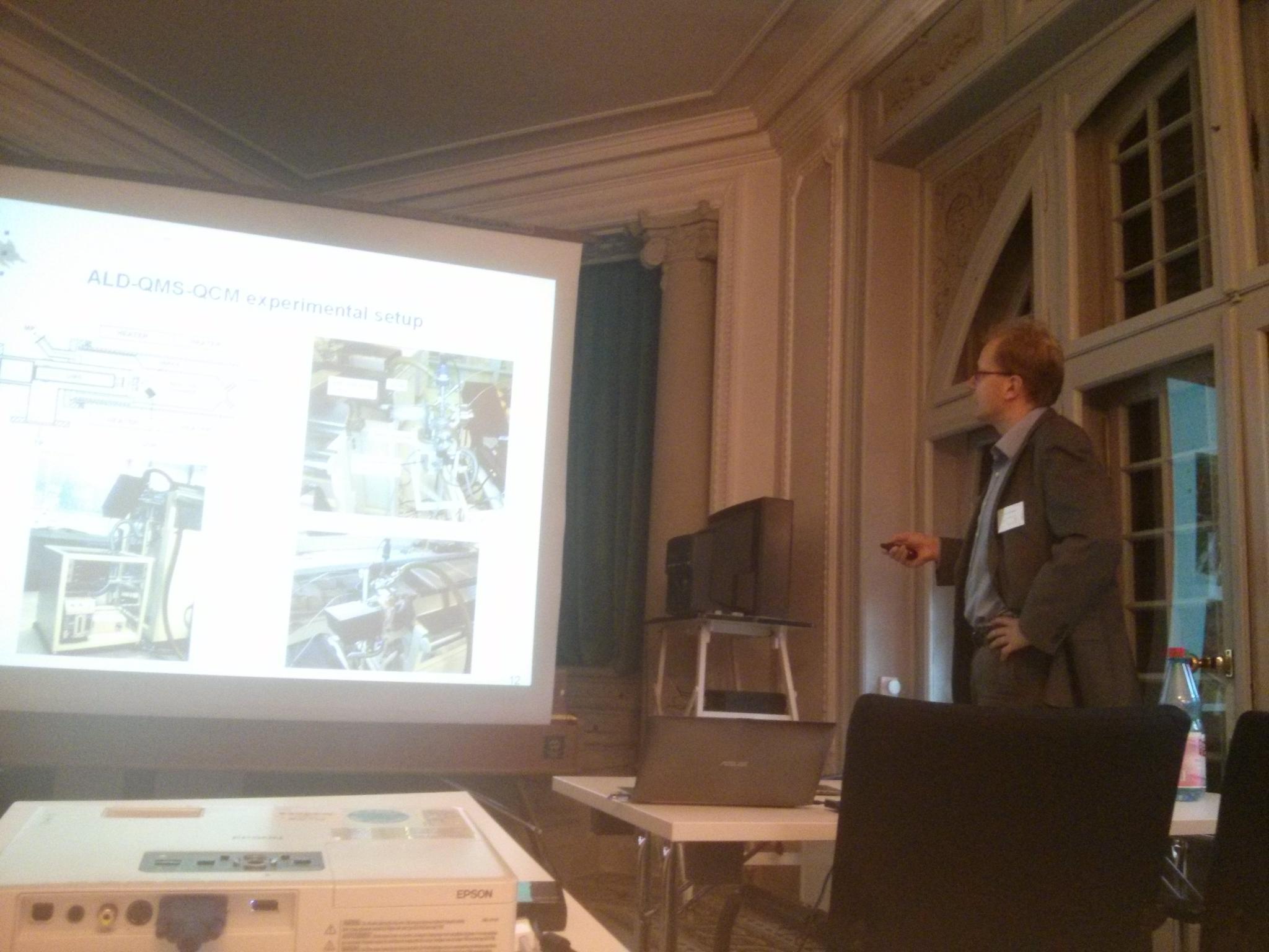
Showing posts with label HERALD. Show all posts

Tuesday, September 6, 2016

Announcement for HERALD Early Career Investigators (ECIs)

To promote the next generation of ALD scientists and help them to establish themselves as research leaders in the ALD community, we have formed a network within HERALD for Early Career Investigators (ECIs). Broadening out the COST definition of ECI, we welcome investigators from within a year of submitting their PhD dissertation to PhD+10 years - however, these are not strict limits.


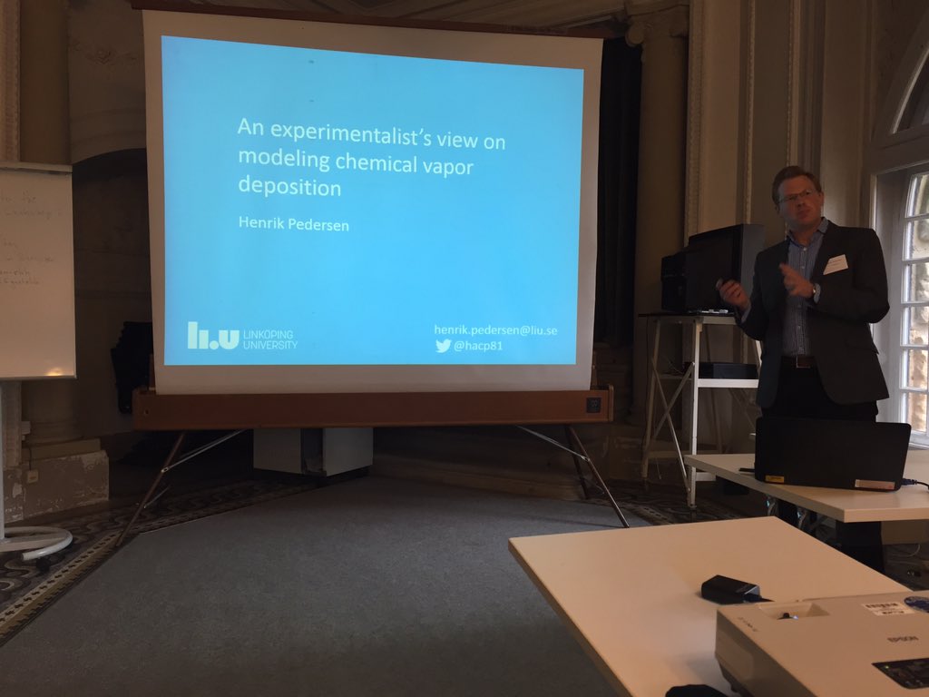
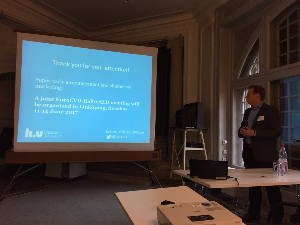
Our ambition is to run workshops where we meet to exchange ideas on career moves, grant applications and possible collaborations. In 2017 we are planning to organize a kickoff event at the Joint EuroCVD-BalticALD conference in Linköping 11-14 June, and a stand-alone workshop where we also invite some senior ALD scientists to give advice on how to establish oneself as an ALD scientist.

If you are interested in joining this network, please contact one of us. 
Henrik Pedersen, henrik.pedersen@liu.se
Jolien Dendooven, jolien.dendooven@ugent.be
Ville Miikkulainen, ville.miikkulainen@helsinki.fi
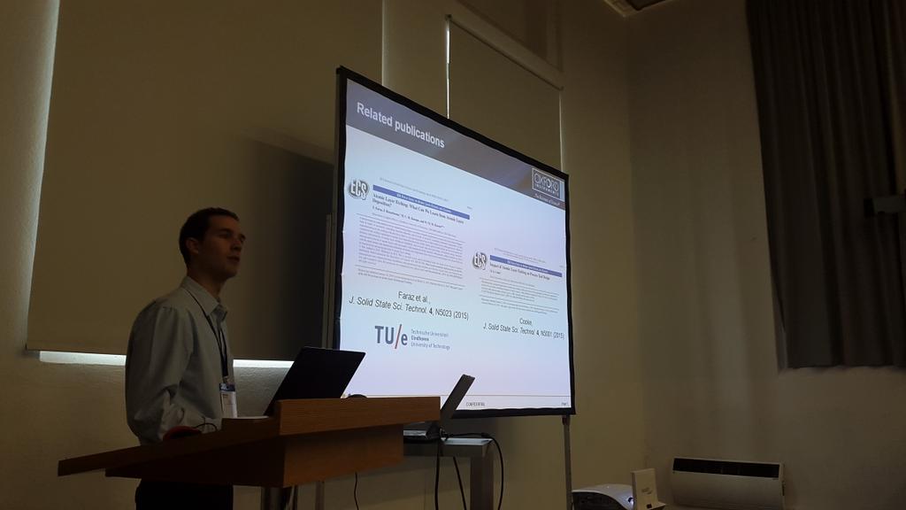
Adrie Mackus, a.j.m.mackus@tue.nl

Sunday, July 17, 2016

2016 General meeting of HERALD at ALD Conference

The 2016 general meeting of the HERALD COST Action MP1402 will take place during the 16th International Conference on Atomic Layer Deposition, which is taking place in the Convention Centre Dublin, Ireland, on 24th-27th July 2016. The final morning of the conference is being devoted to HERALD, in parallel with other conference sessions.

27th July 2016, Liffey Hall 1:

8:45-10:15 HERALD Showcase: Presentation by working group leaders of scientific collaborations in each WG, with opportunity for discussion from all members. Discussion of HERALD targets for widening participation and structuring the ALD community in Europe in the future.

10:15-11:00 HERALD Poster Session: Opportunity for all members to display and discuss posters. There will be no review or selection of abstracts, but the intention to display a poster must be indicated via registering on the eventbrite page by 13th July.

11:00-12:30 Launch of HERALD White Paper on 'Atomic-level processing' and panel discussion: A panel discussion on the future of atomic-level processing for European manufacturing, and in the global context. All are welcome to attend and put their questions to the panellists.

The HERALD sessions are open to all delegates of the ALD2016 conference at no extra fee. HERALD members are strongly encouraged to attend. Travel reimbursements through HERALD are not available, except for the collaboration competition that was previously advertised.


Please register your intention to attend part or all of the HERALD sessions via this eventbrite page by 13th July, so as to facilitate seating, catering and poster boards:

https://www.eventbrite.com/e/herald-sessions-at-ald2016-ireland-tickets-26329089014

The password for the eventbrite page is HERALD 

Wednesday, June 1, 2016

ALD2016 Speakers and Conference Programme announced!

The conference programme for the The 16th International Conference on Atomic Layer Deposition, Dublin Ireland can now be viewed here.

Conference Timings:

Sunday 24 July:

Tutorial runs 13:00-17:00 in Convention Centre. Welcome reception that evening in Guinness Storehouse.

Monday 25 July – Wednesday 27 July:


ALD2016 Conference will open at 8:15 in Convention Centre and closes at 17:45 on Wednesday 27 July followed by a gala dinner on Wednesday evening.

Opening plenary invited talk by Prof. Lars Samuelson, NanoLund, Lund University Sweden followed by Prof. Anatolii Malygin, Saint-Petersburg State Institute of Technology, Russia and Ankur Agarwal, Applied Materials, USA.

ALD 2016 Conference Logo
The 16th International Conference on Atomic Layer Deposition (ALD 2016) will be a three-day meeting dedicated to the science and technology of atomic layer controlled deposition of thin films. In every year since 2001, the conference has been held alternately in United States, Europe and Asia, allowing fruitful exchange of ideas, know-how and practices between scientists. This year, the ALD conference will incorporate the Atomic Layer Etching 2016 Workshop, so that delegates at the two events can interact freely. The conference will take place on 24-27 July 2016 at the Convention Centre Dublin, Ireland.

Atomic Layer Deposition (ALD) is used to fabricate ultrathin and conformal thin film structures for many semiconductor and thin film device applications. A unique attribute of ALD is that it uses sequential self-limiting surface chemistry to achieve control of film growth in the monolayer or sub-monolayer thickness regime. ALD is receiving attention for its applications in leading-edge electronic technologies, advanced microsystems, displays, energy capture and storage, solid state lighting, biotechnologies and medical technologies. Indeed ALD is particularly advantageous for any advanced technology that requires control of film structure in the nanometer or sub-nanometer scale.

As in past conferences, the meeting will be preceded by one day of tutorials. An industry trade show will be held in conjunction with the conference, to act as common ground for academia and industry to meet and discuss the future applications of ALD. Extra opportunities for collaboration will be provided through working groups of the COST Action ‘Hooking together European research in atomic layer deposition (HERALD)’.

This conference offers an excellent opportunity to learn about the most recent R&D activities in ALD science and technology from researchers around the world. We look forward to your participation.

ALD 2016 Co-Chairs:
Simon Elliott, Tyndall National Institute , Ireland Jonas Sundqvist, Division of Solid State Physics, Lund University, Sweden
Simon Elliott
Tyndall National Institute,
Ireland
Jonas Sundqvist
Division of Solid State Physics,
Lund University, Sweden

Saturday, May 28, 2016

HERALD Training School on Atomic Layer Deposition 2-4 July 2016 July 2016, at Thessaloniki, Greece.

HERALD COST Action & the ISSON16 co-organize a Training School on Atomic Layer Deposition on 2-4 July 2016 July 2016, at Thessaloniki, Greece.
 
 
Six (6) students will be granted by HERALD COST Action with 650 € to participate to the lectures of the ALD Training School and ISSON16. E-mail your application to Dr. Spyros Kassavetis (skasa@physics.auth.gr). The program will be announced soon.

Deadline for applications: 5th of June 2016 .

The granted students can submit abstract and participate to NANOTEXNOLOGY 2016 Conferences under a special registration fee. The deadline for abstract submission is 5th of June 2015. For more information, you can visit our NANOTEXNOLOGY 2016 website. 


Thursday, May 26, 2016

ALD History Blog: Photos from HERALD WG2 / ALDCoE Helsinki workshop

ALD History Blog: Photos from HERALD WG2 / ALDCoE Helsinki workshop: We had a very fine HERALD/ALDCoE workshop in Helsinki early this week. About ninety people were present from four continents.


Riikka Puurunen pitching the VPHA organizational poster. Photo by Oili Ylivaara (Twitter via @rlpuu

Excellent invited talks were delivered e.g. by:
  • Prof. Marc Heyns, IMEC, Belgium, 
  • Dr. Simon Rushworth, EpiValence, UK
  • Dr. Paul Williams, Pegasus Chemicals, UK
  • Dr. David C. Smith, LAM Research, USA 
  • Prof. Christophe Detavernier, Ghent University, Belgium
  • Prof. Anjana Devi, Ruhr University Bochum, Germany
  • Prof. Jaan Aarik,  University of Tartu, Estonia
  • Prof. Erwin Kessels, Eindhoven University of Technology, The Netherlands

Friday, May 13, 2016

HERALD White paper on atomic-level processing

Right now there is a brief window of opportunity to feed in to consultations on the future topics for H2020 funding - in particular, the 2018-2020 workplan for NMPB. Some academic and industrial members of HERALD have therefore put together the enclosed position document on urgent research directions, under the overall heading of 'atomic-level processing'.
The document is public. If you feel it is worthwhile, please circulate it to your colleagues, national/regional funding agencies and in particular to your national contact points and delegates on European committees and technology platforms.

It is hoped that this document will evolve into a "Roadmap for Atomic Layer Processing" over the coming months and years. So please feel free to suggest corrections and improvements. Remember that this is a high-level document aimed at non-experts, not a scientific treatise.
As the next step, we are organising an industry panel discussion on this topic on the morning of Wednesday 27th July at the upcoming ALD2016 conference in Ireland. 

Thursday, April 14, 2016

HERALD Workshop: ALD for Novel Sensors and Biosensors May 11-12, 2016

In collaboration with the EU COST networking project HerALD, National Institute (R&D) of Materials Physics (INCDFM) and National R&D Institute for Nonferrous and Rare Metals (IMNR) invites to the ALD for Novel Sensors and Biosensors Workshop on May 11th and 12th, 2016. Aspects regarding modelling growth chemistry of novel sensorial interfaces based on oxides, nitrides, sulphides (W, V, Se-based) and graphene-like layers, technological processes and physical-chemical characterization of nucleation and growth of layers/structures, new up-scalable methods for synthesis of chemical precursors and hybrid organic/inorganic thin films for biosensors will be discussed. A visit to the experimental synthesis and characterisation facilities of INCDFM will be organized.

PROPOSED TOPICS:

  • Modelling growth chemistry of novel sensorial interfaces based on oxides, nitrides, sulphides (W, V, Se-based) and graphene-like layers
  • Technological processes and physical-chemical characterization of nucleation and growth of layers/structures
  • New up-scalable methods for synthesis of chemical precursors
  • Hybrid organic/inorganic thin films for biosensors

Attachments:

Workshop ALD RO_11-12.05.16.pdf
Workshop HERALD - Preliminary Programme.pdf
Abstract template workshop Bucharest.pdf
Registration Form COST MP 1402 Workshop in Bucharest.pdf
Accomodation and transport.pdf
 
COST Action MP1402 - HERALD
Hooking together European research in Atomic Layer Deposition


Monday, March 14, 2016

Photo show NaMLab Novel High-k Materials Workshop in Dresden

Novel High k Application Workshop 2016

In collaboration with the EU COST networking project HerALD (working group 4), NaMLab invites to the Novel High-k Application Workshop on March 14th and 15th, 2016. New challenges offered by the application of high-k dielectric materials in micro– and nanoelectronics will be discussed by more than 80 participants from industry, research institutes and universities. NaMLab created with the workshop a stimulating European platform for application-oriented scientist to exchange ideas and discuss latest experimental results on MIM-capacitors, process technology, leakage & reliability as well as characterization of high-k dielectrics integrated in silicon based micro– and nanoelectronics. In addition, new results in the field of ALD dielectrics in solar cells, transparent conduction oxides (TCOs) and atomic layer etching (ALE) will be discussed. 

Here are pictures from the Event - Day 1:

Networking / Breaks:


Two of the Sponsors of the event Jamal Belgacem from Strem and Andy Stamm Oxford Instruments


The Precursor Buffé from Strem 


Additional sponsors of the event - Sara Wengström from Swedish FAB Support and Paul Williams from Pegasus disussing precursors with very important customers.

Sessions :

 The speakers lining up with USB sticks to upload their presentations


Dr. Karim Cherkaoui, Nanoelectronic Materials and Devices Group (NMD), Tyndall National Lab, Ireland giving a talk on High-k on III/V semiconductors. 

 
J. Roberts from University of Liverpool - Dielectrics for AlGaN/GaN MISHEMT power electronics 


Dr. Jurgen Schubert Peter Grünberg Institute (PGI-9), Forschungszentrum Jülich - Rare eath oxides on GaN


N. Szabo, NaMLab, Dresden - ALD Al2O3 as a high‐k dielectric material for future GaN power devices.


Max Drescher, Fraunhofer IPMS, Dresden - Deciphering Reliability in High‐K Metal Gate Technology. 


Dr. Elke Erben, Globalfoundries, Dresden - Workfunction tuning and gate stack for 22nm FD‐SOI.


Felix Winkler, TU Dresden - Novel vertical TSV field effect transistor using ALD high‐k gate dielectrics


A. Thomas, IFW Dresden - ALD deposited HfO2‐based magnetic tunnel junctions 

 
M. Godlewski, Acad. of Sc. Warsaw, Poland - High‐k oxides by ALD ‐ from applications in electronics to biology and medicine


J. Van Houdt, Imec - High-k in memory devices.


M.H. Park, SNU, Seol, South Korea - Current understanding of ferroelectricity and field‐induced‐ferroelectricity in (Hf,Zr)O2 films based on first order phase transition theory 


Sunday, January 3, 2016

ALD History Blog: Baltic ALD 2015, Tartu: travel notes by Riikka Puurunen

ALD History Blog: Baltic ALD 2015, Tartu: travel notes by Riikka Puurunen - The 13th International Baltic Conference on Atomic Layer Deposition, Baltic ALD 2015 was organised in Tartu, Estonia, September 28-29, 2015. Conference chairs were Prof. Jaan Aarik and Dr. Kaupo Kukli. Conference website: http://www.bald2015.ee/. Right after the conference, on September 30, 2015, there was the yearly meeting day of the HERALD COST network on ALD (http://www.european-ald.net/). I have not visited Tartu before, and it was very interesting to attend this Baltic ALD conference in the historical city of Tartu, where the first report of ALD (then, ALE) is from year 1983. ... more »

Thursday, December 17, 2015

Workshop "Synchrotron Radiation to study Atomic Layer Deposition" 13th-15th June 2016

Workshop "Synchrotron Radiation to study Atomic Layer Deposition" 13th-15th June 2016. Save the date! For more information visit the page: https://indico.cells.es/indico/event/63/


The synchrotron facility ALBA, in Barcelona (Spain) and HERALD are organizing the first workshop on Synchrotron Radiation (SR) and ALD.

The high brilliance of a SR light source enables to study the atomic structure of matter as well as its properties. SR-based spectroscopic, scattering, and diffraction techniques are usually quiet fast and have a high degree of accuracy, precision and sensitivity. Therefore, they are very well suited to study ALD growth. However, until now, the use of SR to study ALD has remained a niche activity of a few groups, mostly because of technical obstacles, the limited availability of beam-time and/or issues concerning the use of certain precursors at synchrotron facilities. 

The workshop will take place at ALBA in June 2016 (more information here: https://indico.cells.es/indico/event/63/). Abstract submission will be opened in January 2016. Fee rates will be low for students, in order to facilitate their participation. 

For further information, please contact Massimo Tallarida (mtallarida@cells.es) and check the webpage (https://indico.cells.es/indico/event/63/).

Saturday, December 12, 2015

MAM2016 & HERALD ALD for BEOL Workshop in Brussels March 20th

MAM 2016 will be the 25th in a series devoted to research on materials properties and interactions of interconnect and silicide materials.  Starting as a workshop on refractory metals and silicides in the 1980’s and moving towards materials for advanced metallization in 1995, the 2016 conference also aims to address new challenges in the fields of Materials for Flexible Electronics,


Tuesday, November 10, 2015

Photo show: Workshop Simulation of chemistry-driven growth phenomena for metastable materials

CECAM/Psi-k/HERALD Workshop
Simulation of chemistry-driven growth phenomena for metastable materials


The controlled growth of thin films based on metastable materials by chemistry-driven processes is of high technological importance for topics like semiconductor devices or optical coatings. Computational modelling of this inherently multiscale process is crucial for an atomistic understanding and enables a decoupling and separate optimization of the growth-determining factors of non-equilibrium materials. This workshop will result in a joint effort by experts from different modelling communities covering the necessary length and time scales.

nearby Marburg in Germany from November 08-11, 2015.
 

Organizers

CECAMPsi-kHERALD
 

Photo Show


Awesome talk by Erwin Kessels on the ALD insight available by sum-frequency generation (Twitter, Henrik Pedersen)


Very good talk by @Simon_D_Elliott  pointing out the danger of using too simplified models for ALD (Twitter, Henrik Pedersen)

 
The Twitter master himself: Henrik Pedersen alias @hacp81 giving an invited on CVD (Twittter, Erwin Kessels)

 Henrik Pedersen annoncing EuroCVD and Baltic ALD in Linköping, Sweden, 2017

 
Very nice talk on in situ analysis in ALD by Mikko Ritala (Twitter, Henrik Pedersen)

 
Mahdi Shirazi discuss cooperative effects in ALD
(Twitter, Henrik Pedersen)


Friday, November 6, 2015

EU COST Network HERALD is opening a new call for research visits (STSMs)

HERALD is opening a new call for research visits (STSMs) between now and the end of March 2016.  This is a rolling call - first come, first served.  Visits may last from 5-90 days and the usual level of funding is €2500.  Full information is available at http://www.european-ald.net/about-short-term-scientific-missions


Tuesday, October 6, 2015

Photoshow : ALD Lab Dresden Symposium at SEMICON Europa 2015

SEMICON Europa this year has turned out to be a major event for ALD and exciting nanoelectronic materials research. Here are photos taken from The ALD Day October 6th, 2015!

More details on this event you can find here : http://baldengineering.blogspot.de/2015/10/ald-ale-and-exciting-nanoelectronic.html

We are already looking forward to SEMICON Europa 2016 in Grenoble, France and to co-chair an ALD Sympoium there yet one more time!

SEMICON Europa ALD 2014, Grenoble : http://baldengineering.blogspot.de/2014/10/voila-3rd-ald-lab-dresden-symposium-at.html


Columbus, Tuesday Oct 6, 13:45, ALD / ALE Sympoium of The ALD Lab Dresden, Messe Dreaden, Germany


Waiting for the ALD Storm!


Welcome
Prof. Johann W. Bartha, TU Dresden


In situ monitoring of Atomic Layer Deposition in porous materials
Martin Knaut, TU Dresden


Passivation of MEMS by Atomic Layer Deposition
Matthias Schwille, Robert Bosch


Symposium is full - please help me throw out a PVD guy


Growth Monitoring by XPS and LEIS Investigations of Ultrathin Copper Films Deposited by Atomic Layer Deposition
Dileep Dhakal, TU Chemnitz/FhG ENAS


High-k dielectrics by ALD for BEOL compatible MIM
Wenke Weinreich, FhG IPMS-CNT


ALD coatings for applications as permeation barrier and protective layer in fiber-reinforced materials
Mario Krug, FhG IKTS


ALD for solar cell application
Ingo Dirnstorfer, NaMLab


Plasma enhanced ALD process for TiO2- and WO3- films
Alexander Strobel, FH Zwickau


Why do we need Atomic Layer Etching
Jonas Sundqvist, Lund University/TU Dresden


Spatial Atomic Layer Deposition and Atomic Layer Etching
Prof. Fred Roozeboom, TU Eindhoven / TNO Eindhoven


Atomic Layer Etching: What Can We Learn from Atomic Layer Deposition?
Harm Knoops, Oxford Instruments/TU Eindhoven


Hardmask and side wall protection during dry etching with plasma enhanced deposition during dry etching for ALE purposes
Stephan Wege, Plasway


Industrial High Throughput Atomic Layer Deposition Equipment and Process for OLED Encapsulation
Jacques Kools, Encapsulix


Monolayer controlled deposition of 2D transition metal dichalcogenides on large area substrates
Annelies Delabie, Imec


Selective Deposition as Enabler for Shrinking Device Dimensions

Suvi Haukka, Executive Scientist, ASM Microchemistry Ltd.