Thursday, June 16, 2022

Electronic Gases Markets – To Approach a US$9 Billion Market in 2022

New materials and increasing chip design complexity drives supply-chain problems for Specialty Gases, Rare Gases and Helium

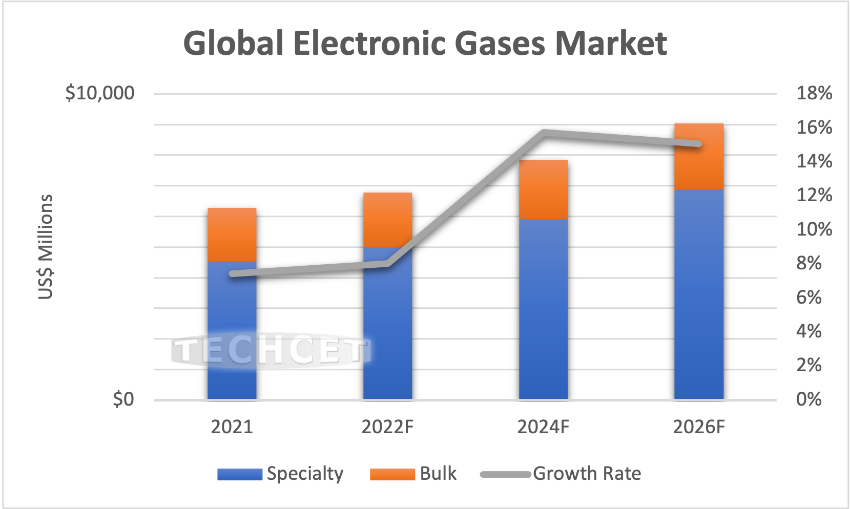
San Diego, CA, June 15, 2022: TECHCET—the electronic materials advisory firm providing business and technology information— reports that the Electronic Gases market revenues hit US$6.3 billion in 2021 and is forecasted to grow to 8% in 2022. In its recently completed Electronic Gases Report , TECHCET forecasts the 2022 Electronic Gases market will reach almost US$6.8 billion—growth primarily attributed to Specialty Gases. As leading-logic and new generations of memory continue to ramp, Specialty Gases consumed in etching, deposition, chamber cleaning, and other applications remain in strong demand. This segment is forecasted to increase by 10% in 2022 with ~9% CAGR through to 2026, as indicated in TECHCET’s newly released 2022 Critical Materials Report™ on Electronic Gases, authored by Jonas Sundqvist, PhD.


In the near-term, there are supply issues for key industry gases, such as helium and neon; and in the longer term, the supply/demand balance for gases such as nitrogen trifluoride (NF3), tungsten hexafluoride (WF6), and others could tighten as industry demand grows.

Neon supply capacity is at risk due to the Russian invasion of Ukraine. Some gas supply from these sources may be at a permanent loss. Helium supply-chain disruptions stemming from lack of Russian supply availability are starting to have an impact on the semiconductor industry. Russia’s current export ban on helium and rare gases will prolong the supply-chain issues with Helium and rare gases like Neon. The war is only part of the helium supply issue – maintenance problems, delayed product availability, and production disruptions in other helium producing regions are all adding to the tightness in the supply chain.

As new semiconductor device fabs come online globally over the next several years, supply constraints may appear for other gases (B2H6, WF6, NF3, CF-gases) since demand increases are expected to outpace supply. With semiconductor manufacturers increasing fab production capacity, the demand for diborane (B2H6) material is rapidly increasing as it is critical in many device applications such as in doped carbon hard masks.

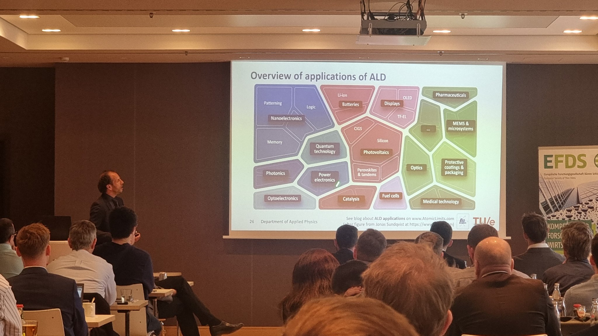
As more CVD/ALD deposition process passes are added for multi-patterning and EUV-lithography, cleaning demand is increasing, thus we anticipate huge growth in NF3 (used for chamber cleaning). With the current projections, demand may outrun supply causing tightness in NF3 availability come 2025-2026. Similarly, TECHCET estimates there may be supply issues with WF6 around 2025-2026. However, the possibility of molybdenum (Mo) replacing tungsten (W) for memory applications could circumvent any WF6 shortage. WF6 demand is primarily driven by vertical scaling in 3DNAND to higher layer counts, though new interconnect materials could lessen any future supply/demand imbalance.

Among the sources of electronic gases highlighted in TECHCET’s CMR are Air Products, Air Liquide, EMD / Merck, Linde, Matheson Gas, SK Materials, Gazprom, Huate Gas, Peric, and many others. For more details on the Electronic Gases market segments and growth trajectory go to: https://techcet.com/product/gases/

ABOUT TECHCET: TECHCET CA LLC is an advisory services firm focused on process materials supply-chains, electronic materials business, and materials market analysis for the semiconductor, display, solar/PV, and LED industries. Since 2000, the company has been responsible for producing the Critical Material Reports™, covering silicon wafers, semiconductor gases, wet chemicals, CMP consumables, Photoresists, and ALD/CVD Precursors. The Critical Materials Council (CMC) of semiconductor fabricators is a business service offered by TECHCET, and includes materials supplier Associate Members. For additional information about reports, market briefings, CMC membership, or custom consulting please contact info@cmcfabs.org, +1-480-332-8336, or go to www.techcet.com.

Friday, June 10, 2022

Atomic Layer Deposition Expected to Grow to Meet Demand for More-than-Moore Devices and Applications

(Interview by SEMI) Atomic Layer Deposition (ALD) players are poised to seize a new growth opportunity after the chip shortage pushed manufacturers to announce fab capacity expansions worldwide. Geared toward 200mm market needs, 300mm ALD platforms have recently advanced to meet the demand of More-than-Moore (MtM) devices and applications for MEMS, sensors, power and RF devices, photonics. Driven by the wafer production volume increase, ALD solutions are now expected to grow and enter the MtM devices market.


SEMI spoke with Dr. Patrick Rabinzohn, Strategic Development Executive of Semiconductor ALD at Beneq, about the benefits of ALD and shared how Beneq is building a comprehensive ALD product portfolio – from Beneq Transform® to ProdigyTM – covering different device applications and wafer sizes. We also talked about Beneq solutions to customer challenges, thanks to its vision and future trends for MtM devices for ALD.

SEMI: Beneq is already a familiar name in the ALD equipment business. For those new to the brand, please introduce the company.

Rabinzohn: Beneq is the home of atomic layer deposition and has ALD in its DNA. In fact, the very first industrial application of ALD was done in 1984 here on electroluminescent displays – the same location where Beneq still is headquartered today! Beneq was formed in 1984 and today we are a leading provider of ALD solutions for More-than-Moore semiconductor device fabrication with the Beneq Transform®.

Beneq’s state of art applications lab enables proof-of-concept and customer adoption for new ALD processes. Our team of engineers and experts is dedicated to making ALD tools accessible to our customers and partners.

SEMI: Beneq introduced the first Beneq Transform® in late 2019. How has adoption been so far?

Rabinzohn: The Beneq Transform® has revolutionized ALD cluster tools for More-than-Moore semiconductor markets in the EU, the U.S. and Asia since its launch in 2019. As of November 2021, Beneq has seen higher than expected demand for both the Transform and Transform Lite product configurations across key customer regions such as Europe, Japan, China, Taiwan and the U.S. We are super excited to see more customers adopting ALD in their More-than-Moore applications.

Thursday, May 12, 2022

Picosun solution enables stretchable organic electronics manufacturing on large scale

ESPOO, Finland, 12th of May 2022 – Organic electronics enable everyday devices such as displays, lighting and sensors to have high energy efficiency, light weight and low manufacturing costs. These benefits have made organic electronics a mainstream technology today and great steps have been taken to realize the technology’s true potential. Finally, flexible and stretchable circuitry can be fabricated, paving the way for wearable devices and e-textiles.


This technological leap has left behind traditional encapsulation methods, such as heavy glass lids with limited stretchability. The biggest downside of organic electronics, however, is their susceptibility to oxidation by moisture. This moisture ingress can have a direct impact on device performance and longevity. To address this challenge, thin film encapsulation solutions (TFEs) have been introduced as a key technology, heavily relying on vacuum-based thin film deposition techniques like atomic layer deposition (ALD). Ultra-thin ceramic ALD films serve as an effective moisture barrier but can crack under stress unless combined with more elastic molecular layer deposition (MLD) films.

Picosun has brought a stable MLD process to the realm of batch processing with PICOSUN® P-300B ALD tool with batch sizes up to 27 pieces of 200 mm wafers. The results show wafer-to-wafer uniformity of 1% and several Å/min growth rates. When combined with ALD in a nanolaminate, the resulting TFE can resist defects when up to 2% tensile stress is applied and the coatings exhibit a steady-state and effective water vapour transfer rate (WVTR) in a range of 10-6 g/m2*d in ambient conditions, when measured from a very large sample area (3320 mm2) to reflect a real-world application.

“We see immense possibilities for our customers with the Picosun’s proven capabilities of depositing ultra-barrier performance TFEs on large scale. As an example, the future OLED manufacturing can be upscaled without fearing for the reliability of the devices”, states Juhana Kostamo, VP, Industrial Business Area of Picosun Group.

Tuesday, May 10, 2022

Semiconductor Materials at a Critical Tipping Point - Key Industry Issues Revealed

San Diego, CA, May 10, 2022: TECHCET—the electronic materials advisory firm providing business and technology information— held its highly successful and well-attended 2022 Critical Materials Conference in Chandler, Arizona on April 28th and 29th. Over 300 attendees and speakers participated in the event to hear about and to discuss semiconductor material issues and trends that are critical to the entire semiconductor industry supply chain—now and in the future.

2022 CMC Conference Keynote Speaker, John Whitman, Corporate Vice President, Operations Central Team & Procurement at Micron Technologies Corp., and Karey Holland, Ph.D., Sr. Advisor and CMC Conference Co-Chair, TECHCET

The opening keynote for the conference was delivered by John Whitman, Corporate Vice President, Operations Central Team & Procurement; Micron Technologies Corp. and addressed the topic of “Covid Impacts on our Supply Assurance Playbook”. The Covid pandemic and subsequent logistic and other supply chain issues over the past two years have highlighted critical issues for the semiconductor industry. Just-in-time delivery has lessened as a procurement priority, and now manufacturers focus on supply chain stability. It is important for device makers to build their supply chain around Business Continuity Plans (BCP) so to ensure production schedules are maintained.

Industry-wide, there is an opportunity for companies to share information through digitization of supply-chain data. With sharing of information and data, companies across the supply chain can collaborate and solve critical issues with respect to materials delivery and performance, thus optimizing semiconductor processing.

This technical conference includes 5 impactful sessions with focuses on 1) Business Trends & Global Issues, 2) Immediate Challenges of Materials & Manufacturing, 3) Future Challenges for Equipment & Component Processes, 4) Emerging Materials & Processes, and 5) Materials for Advanced Packaging and Heterogeneous Integration.

The Conference has just opened up registration for “After Hours” interaction offering online viewing of presentation videos and pdf downloads, and virtual networking opportunities with other “attendees.”On Day 1, sessions 1 through 3 cover a gamut of topics critical to the semiconductor industry supply chain. Topics from the industry outlook for devices, semiconductor manufacturing equipment and materials, to water supply challenges, green manufacturing initiatives, and workforce development were all discussed.
On Day 2, the event focused on emerging materials applications including materials needed for 3nm and smaller technology nodes as well as material challenges of interposes versus bridges and other issues concerning wafer level modeling materials.

For more information about how to attend the CMC Conference After Hours, go to:

Monday, May 2, 2022

NCD supplied additional ALD equipment for special protective coating

Recently NCD supplied additional ALD equipment to the customer based in Korea. It is for coating products used in semiconductor equipment to protect from corrosion and plasma arcing.

This re-contracted equipment is Lucida GSH Series ALD. It is a fast and efficient ALD protective layer coating system with lower precursor usage than existing equipment. The customer is looking forward to extending the lifetime of high cost products through uniform and high quality ALD coating.

This repeat ordered supply shows that the customer has had confidence in the NCD’s ALD technology and the excellence of the equipment.


<LucidaTM GSH Series ALD>

Friday, April 8, 2022

Sneak Peak Into Our New Equipment Components Session at CMC2022 in Chandler AZ April 27-29

Less than 4 Weeks to go for our CMC Conference, April 27-29, Chandler, AZ! Register Now Before It's Too Late!


Here's a Sneak Peak Into Our New Equipment Components Session

-George Alajajian, Ph.D.,VP Strategic Parts Supply Chain, Intel Corp. presenting on "Consumable Equipment Components Requirements for Leading Edge IDMs"

-Dalia Vernikovsky, CEO & GM, Applied Seals NA, Inc presenting on "Polymeric Sealing Properties, Advances & Limitations"

-Jennifer Braggin, Director, CTO’s Office, Entegris presenting on "New filtration and purification technologies for 3nm and beyond for better contamination control and yield improvement"

-Sami Sneck, Vice President, Advanced ALD, Beneq presenting on “Enhancing yield with ALD coatings for critical chamber components”

Coffee / Networking Break - Sponsor: Coexcell with Raffle Giveaway

-Nicole Rutherford, Product Manager, Greene Tweed presenting on “Large-Area Batch ALD Coatings for Chamber Component Protection”

-Christoph Hemmann, EVP Head of Airfreight Americas Region, DB Schenker presenting on "The Air Cargo Supply Chain of the Future- Challenges and Opportunities"

-Michael Bristol, Sr. Product Manager, CoorsTek presenting on “Trends in High Temp Furnace Components for Power Device Processing”

-Tim Dyer, President, Elcon Precision LLC presenting on "Semiconductor ESC and Ceramic Parts Industry Needs and Technical Challenges"

Click here to register for this information packed critical materials event: https://lnkd.in/gkShiM6s

Want to see the full agenda, click here: https://lnkd.in/gzDna7sy

ALD of almost pure organic polymer (3-4 at% Al) films with stability up to 400 °C

The clever ALD people at Helsinki University just published ALD of almost pure organic polymer (3-4 at% Al) films with stability up to 400 °C. This opens the path to a lot of new cool applications. For instance one could imagine the use of ALD deposited photo resist in the semiconductor industry.


Molecular Layer Deposition of Thermally Stable Polybenzimidazole-Like Thin Films and Nanostructures 
Saba Ghafourisaleh, Timo Hatanpää, Anton Vihervaara, Kenichiro Mizohata, Marko Vehkamäki, Markku Leskelä, Matti Putkonen, Mikko Ritala 

First published: 07 April 2022 https://doi.org/10.1002/admi.202200370

The deposition of polybenzimidazole (PBI)-like thin films by molecular layer deposition is reported here for the first time using isophthalic acid (IPA) and 3,3′-diaminobenzidine (DAB) as monomers and trimethylaluminum (TMA) as a linker precursor. Two precursor pulsing sequences are tested, the ABCB (TMA + IPA + DAB + IPA) and ABC (TMA + IPA + DAB) type MLD processes result in different types of PBI-like films. With the ABCB sequence thin film growth per cycle (GPC) of 6.0 Å is obtained at 225–280 °C, whereas GPC of 7.0 Å is obtained with the ABC sequence. Films are characterized in detail by Fourier transform infrared spectroscopy, scanning electron microscopy, thermogravimetric analysis, time-of-flight elastic recoil detection analysis, and atomic force microscopy. The films have good thermal stability and withstand annealing at 400 °C in both air and nitrogen. PBI nanostructures are prepared by depositing PBI-like film on electroblown polyvinylpyrrolidone fibers and removing the template fibers by annealing or dissolution into ethanol.


Thursday, April 7, 2022

Spatial ALD Day coming up at TU Eindhoven June 9

Wednesday, April 6, 2022

Senior Process Engineer I- Coating at ASM Phoenix AZ

About the job

We’re not like most. We don’t just overcome obstacles – we don’t see them. Instead, we see the potential in every person, and every situation. We don’t wait for opportunity to appear – we create it. Meet ASM. A company that has been searching for people just like you.


Job link: (21) Snr Process Engineer I- Coating | ASM | LinkedIn

Who is ASM?

ASM is a leading, global supplier of semiconductor wafer processing equipment. Our ambitious team is dedicated to delivering innovative technology solutions to the world’s leading semiconductor manufacturers. We have over 2,600 employees based in 14 countries, including Belgium, Japan, Netherlands, South Korea, Singapore, Taiwan and United States. Together we work to develop Epitaxy, ALD, PEALD, Vertical Furnaces and PECVD thin-film deposition technologies for our customers. Our goal is to remain an industry leader by being ahead of what’s next. We accomplish this by focusing on finding collaborative solutions to make integrated circuits, or chips, smaller, faster and even more powerful.

ASM, an inclusive workplace

We at ASM are a truly global organization that works diligently with an open-mind in all areas of our business. We strive for a culture and work style that fosters trust and transparency. We put our people first, and that is how we will continue to succeed. We are an equal opportunity employer and value diversity. We recognize and value the differences between individuals, including gender, ethnicity, religious beliefs, sexual orientation, knowledge and experience, work background, age, skills, amongst others. Recruiting and developing a diverse workforce provides a wide range of perspectives. This enables a culture of continuously exploring and adopting new technological ideas and innovations, and it also enables us to deliver excellent products and service to our clients.

Essential Functions
  • Work with a safety-first mentality
  • Drive ASM process protocol with emphasis and regularly institute or update service solutions to the field
  • Work on assigned CIP projects, develop DOE’s and communicate openly both internally and externally.
  • Focus on refresh of IP for legacy products and influence new design IP.
  • Provide “novelty” to items making them hard to reproduce
  • Improve upon existing design for performance and cost efficiency
  • Generate project scope documentation and prepares specific project reports against identified schedule.
  • Building stakeholder consensus to deliver approach
  • Collaboratively manages global stakeholders including end users, technicians, engineers, procurement, spares, manufacturing, subject matter experts as well as management in both business and / or operations to project specific details.
  • Applies project management principles to produce cooperative and collaborative efforts, deliver business strategic objectives and fill the end customer needs.
  • Consistently provide quality solutions to field and customer personnel and create new BKM’s.
  • Exercise good judgment within broadly defined practices and policies in selecting methods, techniques, tools and evaluation criteria for obtaining desired results
  • Be willing to travel domestically and internationally as required.

Education /Experience
  • BS or MS Degree in Mechanical engineering, Electrical Engineering, Material Science or related degree required.
  • 5+ years of experience in the semiconductor field.
  • Equipment Engineering experience with design, and development of complex mechanical systems including comprehension of: reactors, vacuum systems and chambers, gas delivery systems, abatement systems, pneumatics, water cooling, and circuits required. Ability to implement, maintain, improve electrical instruments, equipment, facilities, components, products, systems and provide novel solutions for the semiconductor equipment industry. Comprehension of PLC's and functionality.
  • Should have a broad based background in analysis and debug of complex electrical and/or mechanical systems
  • Semiconductor capital equipment experience is preferred.
  • Understanding of materials: metals, plastics, surface coatings and surface finishes.
  • Deposition product knowledge a plus (CVD, ALD, EPI, PVD). Knowledge of ASM Emerald tool distinct plus.
  • Design applications Pro/ENGINEER, AutoCAD, and Hands on experience with FEA and CFD analysis preferred. Solid ability to read and understand P&IDs, Electrical, and Mechanical schematics and drawings.
  • Proficiency in ANSI Y14.5 geometric dimension and tolerance.

Skills
  • Ability to rectify a challenging situation and gain customer (Internal and external) confidence
  • Strong positive attitude, ability to work in a team environment and work alone. Able to drive meetings, both internal and external, with excellent internal ASM relations
  • Ability to work responsibly with all ASM resources and departments in a multifunctional high paced atmosphere with minimum supervision on highly complex problems
  • Ability to handle multiple tasks simultaneously and be able to organize and run projects
  • Strong computer skills, working knowledge of MS Word, Excel, PowerPoint, SharePoint, Project, and SAP
  • Drive ASM SOP’s and protocol, able to guide co-workers toward common goals
  • Become an active member of ASM GSS core teams
  • Excellent communication skills; speak and write in a clear and concise manner, and ability to accurately and fully convey issues to peers, management, or customers
  • Strong organizational skills and leadership qualities
  • Accurate, timely reporting
  • Parts tracking, ordering, managing, Setting BOM levels
  • Technical writing background. Ability to create procedures, written in an informative manner that eliminates ambiguity and personal interpretation
  • Training skills, be able to communicate with customers and their employees on maintenance procedures, preventative maintenance, and operating specific equipment. Be the content expert with ability to provide onsite support when needed
  • Process comprehension, be able to understand basics of creating process recipes focusing on the ALD process.
  • Understanding of chemistry interactions with different materials. Gas and liquid chemistry knowledge is a bonus
  • Experience with Equipment installs Organizing/Coordinating trades, SL1, SL2, commissioning and qualifications to specific standards.
  • SPC creation with JMP/Statistical analysis and ability to drive root cause solutions through data driven decisions

From the very start of the semiconductor industry to the present day, we’ve been technology leaders who have pioneered innovation and brought new processes into mainstream manufacturing. We are collaborating, creating, and delivering on our vision – a shared vision to drive innovation with new technologies and delivering excellence with dependable products. By doing this, we’ll create new possibilities for everyone to understand, create and share more of what they love.

Be part of our exciting future and join our team today!

Tuesday, April 5, 2022

Using Vapor Phase Infiltration for Fabricating Membranes with David Bergsman – ALD Stories Ep 11


From the corner of one continent to another, Professor David Bergsman joins Tyler from the University of Washington in Seattle. David discusses his use of vapor phase infiltration as a method of fabricating new membrane structures inspired by his work in Stacey Bent’s lab at Stanford and how he started an ALD lab during a pandemic. 
In this video: 
00:00 – Introduction 
02:01 – David’s Background & MLD 
08:02 – Membrane Fabrication and Property Challenges 
17:19 – Vapor Phase Infiltration 
37:36 – Starting an ALD lab 
48:30 – Ending & Outro 

Follow Professor David Bergsman on Twitter @DavidBergsman and learn about his research group in Seattle at www.bergsmangroup.com

Innovative Spatial ALD system at the LZH can precisely coat complex-shaped optics

New possibilities: The LZH can also coat curved optics uniformly with the innovative Spatial ALD system. This is interesting, for example, for applications in the automotive lighting sector. The system achieves high deposition rates.Thanks to the plasma-based Spatial ALD system, another application that is in high demand in industry has been made economical. Layer systems of uniform thickness can be developed and manufactured much faster than before on curved and structured optics.

The system was developed by the Finnish company Beneq together with the LZH.


Picosun ALD and NYCU in Taiwan enhances micro-LED efficiency

ESPOO, Finland, 5th of April 2022 – Picosun Atomic Layer Deposition (ALD) has played a vital role in enhancing electro-optical characteristics of micro-LEDs in research done by National Yang Ming Chiao Tung University (NYCU) in Taiwan.

The usage of dielectric films as a passivation material is a popular technique to suppress dangling bonds as well as to improve output power and external quantum efficiency in LEDs. The study conducted at NYCU compared III-Nitride micro-LEDs of different sizes with and without ALD Al2O3 passivation. The results showed external quantum efficiency enhancement of 70% for 5 µm × 5 µm micro-LEDs and 60% for 10 µm ×10 µm micro-LEDs when using ALD Al2O3 passivation.


In addition, to achieve full color display, an inkjet printing to pattern quantum dots automatically has been developed at NYCU. The solution can considerably improve the precision of color pixels and satisfy the high-resolution requirements. Picosun ALD passivation technology was successfully used for preventing the quantum dots from photo-oxidation and degradation. After a 500 hours environmental reliability test, the color gamut remained at excellent level.*

“Micro-LED technology has been the disruptive technology in the next generation displays, and more application areas are emerging its benefits being long lifetime, high power efficiency and high brightness. With quantum dot-based technology micro-LEDs can be used in applications such as virtual and mixed reality as they allow the use of single-color, blue, micro-LED chips resulting in lower manufacturing costs. Our study has proved that ALD passivation plays a key role in upcoming nanometer-scale devices”, says Hao-Chung Kuo, professor at NYCU.

“Picosun’s ALD technology has been production-proven at many prominent LED manufacturers. ALD films’ superior conformality and uniformity, and their ability to ensure reliable, pinhole-free encapsulation even at extremely low film thicknesses is a key benefit. Furthermore, the ALD process can be run at moderate temperatures”, explains Juhana Kostamo, VP, Industrial Business Area of Picosun Group.

Thursday, March 31, 2022

Launch of the ALD & ALE ReviewBase – An easy-to-access overview of all ALD and ALE review papers

The scientific and technological interest in atomic layer deposition (ALD) and atomic layer etching (ALE) has been surging in the last decade and the sheer volume of ALD and ALE papers can make it difficult to get a clear overview. Now AtomicLimits and Prof. Kessels launched the ALD & ALE ReviewBas in Dresden at the annual EFDS ALD for Industry conference.


Link to the new site: ALD & ALE reviews – Atomic Limits


Tutorial and launch of the ReviewBase - ALD: materials, process technologies and applications Prof. Erwin Kessels, TU Eindhoven, NL.


Sunday, March 27, 2022

Call for Papers for the 242nd ECS Meeting, to be held from Oct. 9-13, 2022, symposium G02: Atomic Layer Deposition and Etching Applications

Dear colleagues in Atomic Layer Deposition and Etching,

We hereby send you the Call for Papers for the 242nd ECS Meeting, to be held from Oct. 9-13, 2022, in Atlanta (USA). Especially interesting for you will be symposium G02: Atomic Layer Deposition and Etching Applications 18 that we* are organizing on an annual basis.

*organizers: Fred Roozeboom, Stefan De Gendt ; Jolien Dendooven ; Jeff Elam ; Oscar van der Straten ;Andrea Illiberi ; Ganesh Sundaram ; Rong Chen ; Thorsten Lill ; Oana Leonte ; Matthias Young


Below, you can find the Call for Papers and instructions to submit your abstract.

The due date for submission is Friday April 8, 2022.

Students can apply for (partial) travel support.

More details can be found right below this message.

Kind regards, also on behalf of my co-organizers.
Fred

Prof. dr. Fred Roozeboom
Group Inorganic Membranes
Faculty of Science & Technology
University of Twente
PO Box 217
7500 AE Enschede
The Netherlands
Mobile: +31 6 51375283
f.roozeboom@utwente.nl

Wednesday, March 16, 2022

Additive Manufacturing in Atomic Layer Processing Mode by Atlant 3D

Open Source : Additive Manufacturing in Atomic Layer Processing Mode

Ivan Kundrata,Maïssa K. S. Barr,Sarah Tymek,Dirk Döhler,Boris Hudec,Philipp Brüner,Gabriel Vanko,Marian Precner,Tadahiro Yokosawa,Erdmann Spiecker,Maksym Plakhotnyuk,Karol Fröhlich,Julien Bachmann
First published: 11 March 2022


Additive manufacturing (3D printing) has not been applicable to micro- and nanoscale engineering due to the limited resolution. Atomic layer deposition (ALD) is a technique for coating large areas with atomic thickness resolution based on tailored surface chemical reactions. Thus, combining the principles of additive manufacturing with ALD could open up a completely new field of manufacturing. Indeed, it is shown that a spatially localized delivery of ALD precursors can generate materials patterns. In this “atomic-layer additive manufacturing” (ALAM), the vertical resolution of the solid structure deposited is about 0.1 nm, whereas the lateral resolution is defined by the microfluidic gas delivery. The ALAM principle is demonstrated by generating lines and patterns of pure, crystalline TiO2 and Pt on planar substrates and conformal coatings of 3D nanostructures. The functional quality of ALAM patterns is exemplified with temperature sensors, which achieve a performance similar to the industry standard. This general method of multimaterial direct patterning is much simpler than standard multistep lithographic microfabrication. It offers process flexibility, saves processing time, investment, materials, waste, and energy. It is envisioned that together with etching, doping, and cleaning performed in a similar local manner, ALAM will create the “atomic-layer advanced manufacturing” family of techniques.


AVS ASD 2022 April 21-22 - Technical program


Technical Program
Reserve Hotel by March 25
We have arranged a special conference rate at the Westin St. Francis. Keep in mind that reserving a room in the conference hotel block is important because it helps ASD meet its financial commitments to the host city and retain lower registration fees as well as a high quality conference with the features and services you are accustomed too.

Due to limited space we recommend booking as early as possible to receive this special rate—please note that once the reserved/contracted room block is full, the room availability and rate are not guaranteed and may vary.

If your dates are not available, please contact Alberto Lamberti at 1-415-774-0122, alberto.lamberti@westin.com for help.
In an effort to help facilitate the progression of ASD techniques, the 6th Area Selective Deposition Workshop (ASD 2022) scheduled for April 21-22, 2022, in San Francisco will act as a central event for sharing and discussing the newest developments in ASD by gathering leading experts from both academia and industry. Attendees can expect to participate in talks regarding fundamental challenges related to recent developments in ASD, applications for ASD in next-generation technology, emergent processes for implementing ASD techniques, and new perspectives on metrological and characterization strategies for further understanding persistent mechanistic challenges. Based on the success of the previous workshops, ASD 2022 will consist of two days of presentations by invited and contributing speakers, as well as a banquet reception and poster session.
Invited Speakers:

  • Keynote Speaker - Stacey Bent (Stanford University, USA), "Next Generation Nanopatterning Using Area Selective Deposition”
  • Cathleen Crudden (Queen's University, Canada), "N-heterocyclic Carbenes in Selective Area Deposition"
  • Jolien Dendooven (Ghent University, The Netherlands), "In-situ Studies of Nucleation Mechanisms during ALD of Platinum-Group Metals"
  • Damon Farmer (IBM Research, USA), "Inhibitor-Free Nucleation Inhibition of Superconductors"
  • Padma Gopalan (University of Wisconsin, USA), "Carbon Nanotube Selective Deposition"
  • Andrew Kummel (University of California San Diego), "Selective Atomic Layer Deposition of MoSiX"
  • Mikko Ritala (University of Helsinki, Finland), "Area-Selective Etching of Polymers, a Novel Approach to Self-Aligned Patterning of Thin Films"
  • Frances Ross (Massachusetts Institute of Technology, USA), "In Situ Electron Microscopy to Visualize Crystal Growth Mechanisms on Plain and Patterned Surfaces"
  • Bonggeun Shong (Hongik University, South Korea), "Theoretical Understanding on the Principles of Area-Selective Atomic Layer Deposition"
Topics:
This event is centered on showcasing developments across the whole spectrum of area-selective deposition. Thus, the Workshop will cover a wide range of topics including the following:

  • Near Term Technology Readiness (Scalable and Relevant ASD Processes for Use in Manufacturing)
  • Fundamentals of ASD (Defects, Growth Mechanisms and Inhibitor Chemistries)
  • Metrology Techniques for ASD
  • Emerging/Exploratory ASD Processes and Applications (e.g., Catalysis, Energy Generation and Storage)
Program Chair:
Rudy J. Wojtecki
IBM Almaden Research Center, USA
Questions? Contact rjwojtec@us.ibm.com