Thursday, March 31, 2022

Launch of the ALD & ALE ReviewBase – An easy-to-access overview of all ALD and ALE review papers

The scientific and technological interest in atomic layer deposition (ALD) and atomic layer etching (ALE) has been surging in the last decade and the sheer volume of ALD and ALE papers can make it difficult to get a clear overview. Now AtomicLimits and Prof. Kessels launched the ALD & ALE ReviewBas in Dresden at the annual EFDS ALD for Industry conference.


Link to the new site: ALD & ALE reviews – Atomic Limits


Tutorial and launch of the ReviewBase - ALD: materials, process technologies and applications Prof. Erwin Kessels, TU Eindhoven, NL.


Sunday, March 27, 2022

Call for Papers for the 242nd ECS Meeting, to be held from Oct. 9-13, 2022, symposium G02: Atomic Layer Deposition and Etching Applications

Dear colleagues in Atomic Layer Deposition and Etching,

We hereby send you the Call for Papers for the 242nd ECS Meeting, to be held from Oct. 9-13, 2022, in Atlanta (USA). Especially interesting for you will be symposium G02: Atomic Layer Deposition and Etching Applications 18 that we* are organizing on an annual basis.

*organizers: Fred Roozeboom, Stefan De Gendt ; Jolien Dendooven ; Jeff Elam ; Oscar van der Straten ;Andrea Illiberi ; Ganesh Sundaram ; Rong Chen ; Thorsten Lill ; Oana Leonte ; Matthias Young


Below, you can find the Call for Papers and instructions to submit your abstract.

The due date for submission is Friday April 8, 2022.

Students can apply for (partial) travel support.

More details can be found right below this message.

Kind regards, also on behalf of my co-organizers.
Fred

Prof. dr. Fred Roozeboom
Group Inorganic Membranes
Faculty of Science & Technology
University of Twente
PO Box 217
7500 AE Enschede
The Netherlands
Mobile: +31 6 51375283
f.roozeboom@utwente.nl

Wednesday, March 16, 2022

Additive Manufacturing in Atomic Layer Processing Mode by Atlant 3D

Open Source : Additive Manufacturing in Atomic Layer Processing Mode

Ivan Kundrata,Maïssa K. S. Barr,Sarah Tymek,Dirk Döhler,Boris Hudec,Philipp Brüner,Gabriel Vanko,Marian Precner,Tadahiro Yokosawa,Erdmann Spiecker,Maksym Plakhotnyuk,Karol Fröhlich,Julien Bachmann
First published: 11 March 2022


Additive manufacturing (3D printing) has not been applicable to micro- and nanoscale engineering due to the limited resolution. Atomic layer deposition (ALD) is a technique for coating large areas with atomic thickness resolution based on tailored surface chemical reactions. Thus, combining the principles of additive manufacturing with ALD could open up a completely new field of manufacturing. Indeed, it is shown that a spatially localized delivery of ALD precursors can generate materials patterns. In this “atomic-layer additive manufacturing” (ALAM), the vertical resolution of the solid structure deposited is about 0.1 nm, whereas the lateral resolution is defined by the microfluidic gas delivery. The ALAM principle is demonstrated by generating lines and patterns of pure, crystalline TiO2 and Pt on planar substrates and conformal coatings of 3D nanostructures. The functional quality of ALAM patterns is exemplified with temperature sensors, which achieve a performance similar to the industry standard. This general method of multimaterial direct patterning is much simpler than standard multistep lithographic microfabrication. It offers process flexibility, saves processing time, investment, materials, waste, and energy. It is envisioned that together with etching, doping, and cleaning performed in a similar local manner, ALAM will create the “atomic-layer advanced manufacturing” family of techniques.


AVS ASD 2022 April 21-22 - Technical program


Technical Program
Reserve Hotel by March 25
We have arranged a special conference rate at the Westin St. Francis. Keep in mind that reserving a room in the conference hotel block is important because it helps ASD meet its financial commitments to the host city and retain lower registration fees as well as a high quality conference with the features and services you are accustomed too.

Due to limited space we recommend booking as early as possible to receive this special rate—please note that once the reserved/contracted room block is full, the room availability and rate are not guaranteed and may vary.

If your dates are not available, please contact Alberto Lamberti at 1-415-774-0122, alberto.lamberti@westin.com for help.
In an effort to help facilitate the progression of ASD techniques, the 6th Area Selective Deposition Workshop (ASD 2022) scheduled for April 21-22, 2022, in San Francisco will act as a central event for sharing and discussing the newest developments in ASD by gathering leading experts from both academia and industry. Attendees can expect to participate in talks regarding fundamental challenges related to recent developments in ASD, applications for ASD in next-generation technology, emergent processes for implementing ASD techniques, and new perspectives on metrological and characterization strategies for further understanding persistent mechanistic challenges. Based on the success of the previous workshops, ASD 2022 will consist of two days of presentations by invited and contributing speakers, as well as a banquet reception and poster session.
Invited Speakers:

  • Keynote Speaker - Stacey Bent (Stanford University, USA), "Next Generation Nanopatterning Using Area Selective Deposition”
  • Cathleen Crudden (Queen's University, Canada), "N-heterocyclic Carbenes in Selective Area Deposition"
  • Jolien Dendooven (Ghent University, The Netherlands), "In-situ Studies of Nucleation Mechanisms during ALD of Platinum-Group Metals"
  • Damon Farmer (IBM Research, USA), "Inhibitor-Free Nucleation Inhibition of Superconductors"
  • Padma Gopalan (University of Wisconsin, USA), "Carbon Nanotube Selective Deposition"
  • Andrew Kummel (University of California San Diego), "Selective Atomic Layer Deposition of MoSiX"
  • Mikko Ritala (University of Helsinki, Finland), "Area-Selective Etching of Polymers, a Novel Approach to Self-Aligned Patterning of Thin Films"
  • Frances Ross (Massachusetts Institute of Technology, USA), "In Situ Electron Microscopy to Visualize Crystal Growth Mechanisms on Plain and Patterned Surfaces"
  • Bonggeun Shong (Hongik University, South Korea), "Theoretical Understanding on the Principles of Area-Selective Atomic Layer Deposition"
Topics:
This event is centered on showcasing developments across the whole spectrum of area-selective deposition. Thus, the Workshop will cover a wide range of topics including the following:

  • Near Term Technology Readiness (Scalable and Relevant ASD Processes for Use in Manufacturing)
  • Fundamentals of ASD (Defects, Growth Mechanisms and Inhibitor Chemistries)
  • Metrology Techniques for ASD
  • Emerging/Exploratory ASD Processes and Applications (e.g., Catalysis, Energy Generation and Storage)
Program Chair:
Rudy J. Wojtecki
IBM Almaden Research Center, USA
Questions? Contact rjwojtec@us.ibm.com

Thursday, March 10, 2022

Beneq fulfills customer demand for tailored ALD equipment services and support with BeneqCareTM

Beneq, the home of Atomic Layer Deposition (ALD), has introduced BeneqCare, a new modular solution to offer support and maintenance services to organizations that own and operate Beneq ALD equipment.

Beneq leads the market with ALD products for R&D, semiconductor device fabrication, 3D and batch production, ultra-fast spatial ALD (C2R), and roll-to-roll ALD. Today, the company has launched BeneqCare to help customers in the EU, Asia and the USA maximize the value of their ALD tools throughout their equipment’s life cycles.


“We have been investing heavily in widening our service capabilities worldwide. Now, we offer service coverage in all regions. We have also established spare part hubs in every region at Beneq offices,” says Hans Fabritius, Vice President, Life Cycle Services at Beneq.

“BeneqCare simplifies ALD equipment ownership by helping our customers maximize uptime and gain access to the right support at every stage of their tool’s life cycle. We are ready to assist our customers in meeting their productivity requirements –from training personnel in using the equipment to meeting any unscheduled maintenance or spare parts needs,” asserts Fabritius.

BeneqCare provides Beneq customers who operate in the industrial and research sectors with a wide range of service modules to suit their operations, from extended warranty and training services to remote or onsite support.

“Our customers have high expectations for the performance of their Beneq ALD tools. BeneqCare brings them versatile support and service plans that grow with their businesses,” says Fabritius.

Companies and research facilities that have commissioned Beneq ALD equipment can avail of a variety of BeneqCare service modules to suit their unique requirements. Among the BeneqCare modules are technical support services, including remote support via Augmented Reality (AR); spare part services; extended warranties; preventive as well as unscheduled maintenance services; and training.

Learn more about BeneqCare.


Tuesday, March 8, 2022

RASIRC Granted Patent for Controlled Delivery of Hydrogen Peroxide Gas

Novel method for generation of H2O2 gas granted patent in US and Japan


San Diego, California – February 24, 2022 – RASIRC announced that the United States Patent and Trademark Office has granted Patent # US 11,154,792 B2 for a novel Method, System and Device for Delivery of Process Gas. The patent is applicable to RASIRC hydrogen peroxide products including the Peroxidizer®. The patent was also certified by the Japan Patent Office as Patent 6951321. The method enables more accurate and repeatable delivery of hydrogen peroxide gas into a wide range of flow rates, operating pressures, and temperatures.


This invention correlates instantaneous applied power to mass delivery of H2O2, largely eliminating nonuniformities in the liquid source and thermal droop. This enables the Peroxidizer to provide accurate and linear delivery of chemistry without regard to vaporization temperature or process pressure.

“By applying this new process control method, the Peroxidizer can provide linear control throughout the mass flow range independent of the carrier gas flow rate and operating pressure of the process,” said RASIRC Founder and CEO Jeffrey Spiegelman. “This design integrates custom hardware, firmware and software to improve both Peroxidizer performance and tool-to-tool repeatability, helping us meet the semiconductor standards for high volume manufacturing (HVM).”

Power control is a very effective way to deliver vapor from a liquid source. Most liquid to vapor mass flow control is managed by temperature regulation of the liquid source or bath. However, bath temperature increases with increased mass flow rate causing temperature non-uniformities, localized droop, and output instabilities. As the temperature increases the vapor pressure increases on a power curve. Error increases in a highly non-linear fashion. For example, H2O2 vapor pressure change of 1°C at 90°C is 20 times larger than 1°C at 30°C, leading to 20X increased error at the higher temperature. Power control is based on the mass evaporated so the error does not increase with increasing bath temperature.

About the RASIRC Peroxidizer®

The RASIRC Peroxidizer provides a safe, reliable way to deliver high-concentration hydrogen peroxide gas into ALD, annealing, gapfill, dry surface preparation, and cleaning processes.

About RASIRC

RASIRC transforms liquids into dynamic gases that power process innovation in semiconductor and adjacent markets. By commercializing molecules for lower temperature processes, RASIRC patented technology enables the manufacture of atomic-scale oxides, nitrides, and metals. Innovative products such as Brute Peroxide, Brute Hydrazine, the Peroxidizer, and the Rainmaker Humidification Systems are being used to develop solutions for 5G, AI, IOT, and advanced automation.

What makes RASIRC a unique industry leader is our technical expertise and commitment to solving complex industry challenges for our customers. Our team of industry experts has a proven track record of beating larger competitors to market by efficiently delivering state of the art technology that reduces cost, improves quality, and dramatically improves safety. With our customers at the forefront of all we do, we continue to research, develop, and design innovative products that purify and deliver ultra-pure gas from liquids for the semiconductor and related markets. Contact RASIRC to help solve your complex problems.


P: 858-259-1220, email info@rasirc.om or visit http://www.rasirc.com

Saturday, March 5, 2022

The Emergence of Hydrazine (N2H4) in Semiconductor Applications


The Emergence of Hydrazine (N2H4) in Semiconductor Applications
by Jeffrey Spiegelman and Daniel Alvarez

 Purpose

Historically, metal-nitride MOCVD and ALD films have been fabricated with Ammonia (NH3).  However, lower thermal budgets and shrinking 3-dimensional structures are needed for next generation semiconductor devices.  These challenges have exposed limitations with ammonia which could be overcome by replacing ammonia with hydrazine (N2H4).  Purity of commercially available hydrazine has  delayed its adoption.  RASIRC Inc. has recently developed a new formulation of hydrazine called BRUTE® Hydrazine which is safer and meets purity requirements for semiconductor manufacturing. Prior to Brute Hydrazine, the body of technical data applicable to semiconductor processing was limited and scattered.  This paper provides an overview of the growing activity in the thin film use of Brute hydrazine as well as early references on laboratory grade hydrazine for historical completeness.


Increasing Need for More Reactive Nitrogen Sources

Emerging devices such Logic and Advanced Memory require high quality thin (5-20 Å) electrode and barrier films.  Difficult thermal budget constraints are now being placed on well-known materials such as SiNx, TiNx and TaNx.1-3  Deposition temperature limitations have dropped to 350°C and below while very low resistivity (<150 micro-ohm/cm) for TiN and TaN must still be achieved.   Although metal and nitride films grown using plasma assisted processes (PE-ALD) and (PE-CVD) at low temperatures exhibit enhanced properties, the damage induced by plasma on sensitive substrates is one of the common drawbacks,4,5 as well as inability to support HAR or three-dimensional structures like horizontal vias and deep trenches.

III-V Nitride devices require a more reactive nitrogen source to reduce deposition temperatures and increase compositional stability.6 Growth rates for InGaN films deposited with ammonia at reduced temperatures are prohibitively slow and grossly inefficient in ammonia usage. A more reactive nitrogen source can enable acceptable deposition rates at 500-650° C, where alloy stability is significantly increased and nitride source to precursor ratio can be reduced.

In addition to growing thin nitride films, hydrazine can also act as a reducing agent for several late transition-metals.  This work is highly relevant to the use of hydrazine as a surface cleaning agent as well as a potential adder for metal ALD.7


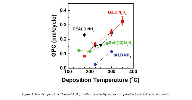
Figure 1: Low Temperature Thermal ALD growth rate with Hydrazine comparable to PEALD with Ammonia.

The following table provides primary references for the areas of hydrazine ALD/CVD relevant to Semiconductor device applications.  Additional relevant references on related films are also included.


Precursor and Temperature

Film

Reference

Al surface nitridation

200C-450C

AlN

Taylor et.al.  U.S. Patent 6465350, 2002

TMA MOCVD  300C-400C

AlN

Fujieda, S. et. al.   Adv. Func. Mat.  1996, 6(3), 127-134

TDEAA  150C-225C

AlN

Abdulagatov, A.I.  et. al. Russian Microelectronics, 2018, 47(2), 118–130.


TMA 175C-350C

AlN

Jung, Y.C.  et. al. Materials 2020, 13, 3387;

 https://doi:10.3390/ma13153387


TDMAA 225C-400C

AlN

Ueda, S.T. et. al.  Appl. Surf. Sci.  2021, 554, 149656

BCl3 ,  350C

BN

Wolf, S. et. al. Appl. Surf.  Sci.   2018, 439, 689–696

Surface Clean

200C

Cu

Hwang, S.M.  et. al. ECS Trans. 2019, 92, 265


Surface Clean 100C-300C

Cu, Co

Hwang, S.M. “Effect of Surface Cleaning Efficacy on Vapor-Phase Cleaning of Cu and Co Using Anhydrous N2H4AVS ALD/ALE 2021 Session: Area Selective ALD AS4-1

TMG, 400C-800C

GaN

Fujieda, S.  et. al. Jpn. J. Appl. Phys.  1987, 26, 2067-2071


TMG, TMI, 600C-900C Theoretical

GaN, InGaN

Koukitu, A. et. al. phys. Stat. sol. (b), 1999, 216(1), 707-712


TMG

Theoretical

GaN

Goddard, W. et.al. J. Phys. Chem. C 2015, 119(8) 4095–4103


[Ru(DMBD)(CO)3]

200C. Metal Deposition

Ru

Cwik, S. et. al.  J. Vac. Soc.  Sci. & Tech. A 2020, 38, 012402; https://doi.org/10.1116/1.5125109

SiH4   550C-1050C

SiN

Yoshioka, S. et. al.   J. Electrochem. Soc. 1967, 114, 962–964.

SiH4/W hot wire  300C

SiN

Matsumura, H. 1989 Jpn. J. Appl. Phys. 28 2157

Si2H6, Si3H8 

350C-550C

SiN

Kanoh, H.  et al.  “Low-Temperature Chemical-Vapor-Deposition of Silicon Nitride” Journal de Physique IV Proceedings, 1991, 02 (C2), pp.C2-831-C2-837.

Si surface Nitridation.

300C-500C

SiN

Abyss, J.A. et. al.  J. AIChE  1995, 41, 2282–2291

Si2Cl6  285C

SiN

Edmonds, M. et. al.,   J. Chem. Phys. 2017, 146, 052820 ;  https://doi.org/10.1063/1.4975081

Si2Cl6  320C-410C


SiN

Kondusamy, A.  et. al.Low Temperature Thermal ALD of Silicon Nitride Utilizing a Novel High Purity Hydrazine Source”, Electrochem. Soc. AiMES 2018, Meet. Abstr.  G02-993

Si2Cl6  410C-650C

SiN

Le, D.N. et al “Thermal Atomic Layer Deposition of Silicon Nitride Using Anhydrous Hydrazine and Ammonia” AVS ALD 2021, Session AF9.

TBTDET 150C-250C

TaN

Burton, B.B., et. al. J. Electrochem. Soc. 2008, 155, D508

TBTDET 100C-300C

TaN

Wolf, S. et.al.  Appl. Surf. Science, 2018, 462, 1029-1035

TDMAT  200C

TiN

Wierda, D.A. et. al. Electrochemical and Solid-State Letters, 1999, 2 (12) 613-615

TiCl4  200C-350C

TiN

Abdulagatov, A.I.  Ph.D. Thesis, Univ. of Colorado, 2012, UMI No. 3549153

TiCl4  300C-400C

TiN

Wolf, S. et.al.  Appl. Surf. Science, 2018, 462, 1029-1035

TiCl4  300C-400C

TiN

 Kuo, C.H. et. al.Low Resistivity Titanium Nitride Thin Film Fabricated by Atomic Layer Deposition on Silicon”

  AVS ALD 2021, Session AM5-9.

TiCl4  250C-400C

TiN

Alvarez, D. et. al.  “Comparative Study of Titanium Nitride ALD using High Purity Hydrazine vs Ammonia” Electrochem. Soc. 2020 Meet. Abstr. MA2020-02 1668

BTBMW

300C

WN

Bernal-Ramos, K.   Ph.D. Thesis, Univ. of Texas, Dallas, 2014,

UMI  No. 3668896

BTBMW

250C-350C

WN

Le, D.N.  et.al. “Atomic Layer Deposition of Nanometer Thick Tungsten Nitride Using Anhydrous Hydrazine for Potential X-Ray Optics Application” AVS ALD/ALE 2021 Session: AF10-15

Discussion on Specific Films

Titanium Nitride (TiN) is a critical film in semiconductor manufacturing. Commonly TiN is utilized as an electrode material as well as a low resistivity barrier layer.  Early CVD work by Wierda demonstrated low temperature (50C-250C) TiN CVD by hydrazine and TDMAT.  Optimal results were obtained when 1.9% hydrazine was combined with ammonia.  This may be attributed to a different mechanistic pathway or ammonia dilution of oxygen containing contaminants.  Wolf later demonstrated low temperature (300C) TiN ALD with the use of TiCl4. This result was then optimized by Kuo in the same lab, where resistivities well below 180 micro-ohm/cm were achieved by reducing oxygen contamination in the film through improved hydrazine purity. A comparative study of Hydrazine vs Ammonia for TiCl4 was reported by Taiyo Nippon Sanso, where the two nitrogen sources showed highly disparate growth rates and film properties.  Hydrazine demonstrated viability at the 250C-400C range for low temperature semiconductor applications.

Silicon Nitride (SiN) is a widely used material in semiconductor devices. SiN is commonly used as an etch stop, a dielectric layer, an encapsulation layer, and as a barrier layer on organic devices.  As early as 1967, hydrazine and Silane CVD was demonstrated at 550C.  This work was then followed-up by Kanoh with higher silanes in the 350C-550C range.  In a very interesting approach, Abyss demonstrated Si surface nitridation with hydrazine at temperatures as low as 300C.  More recently, Edmonds cleverly used hydrazine/hexachlorodisilane ALD to place a thin SiN passivation layer on SiGe at 285C.  Extensive studies have been carried out by the Kim group at UT Dallas in the range of 320C-650C.  Below 400C, thermal ALD leads to films with good composition, but unfavorable low density and high wet etch rates.  This can be overcome with addition of Argon plasma densification.  At 480C and above, thermal ALD films are grown with high density, low wet etch rates, and reduced hydrogen incorporation.  When compared to ammonia grown films in the same temperature range, the hydrazine ALD films are superior up to temperatures >600C where films properties become more similar.

Gallium Nitride and Indium Gallium Nitride (GaN, InGaN) grown with hydrazine have had few publications in the last 20 years despite interest in reduction of ammonia usage and poor indium incorporation. These films are central in LEDs and emerging power devices.  Fujieda demonstrated that overall chemical consumption can be greatly reduced with hydrazine vs ammonia for GaN deposition in the 400C-800C range.  Koukitu followed this up with a theoretical thermodynamic study showing how the use of hydrazine can reduce deposition temperature and stabilize composition for GaN and InGaN films.  In 2015, Goddard elucidated the likely mechanisms for hydrazine vs ammonia is GaN deposition.

Though little has been published for GaN/InGaN deposition with hydrazine, viability for III/V materials can be inferred from work published for AlN ALD with hydrazine.  Fujieda reported MOCVD with trimethyl aluminum (TMA) in the 300C-400C range.  More recently Jung reported ALD with TMA as low as 175C and compared to ammonia in the 175C-350C range.  Abdulagatov made use of the nitride-based ligands with TDEAA/hydrazine ALD in the 150C-250C range.  In a similar approach using TDMAA, Ueda has reported the deposition of crystalline AlN films as low as 350C with thermal ALD.  With the addition of Argon plasma densification, crystalline films can be obtained as low as 225C, where crystallinity in AlN was optimized at 400C.

Copper, Cobalt and Ruthenium can be reduced in situ by Hydrazine.  Furst provided a detailed review on hydrazine as a reducing agent for organic compounds.8 Recently Hwang reported an extension of this reactivity to Cu surfaces.  Gas phase reduction of Cu oxides to Cu metal with hydrazine at moderate temperatures (100C-300C) was reported.  Here, hydrazine is introduced in short pulses, analogous to an ALD reaction. A similar report for Cobalt has also been presented by Hwang.  Cwik working in the Winter group has recently released data showing the ability to grow Ru metal using hydrazine as a reducing agent in Ru ALD at 200C.  Here hydrazine was found to be advantageous over substituted hydrazine derivatives.

Conclusion

Hydrazine is emerging as a replacement for ammonia in low temperature applications.   Recent examples of different production-worthy nitrides have been reported for both ALD and MOCVD films.  These positive reports have led to an increasing level of interest within the scientific community looking for solutions to new device structures and increased density.

Contact the Author

The author is available for additional technical discussion. Contact RASIRC to schedule an appointment.

References

1. Burton BB, Lavoie AR, George SM (2008) Tantalum nitride atomic layer deposition using (tert-Butylimido) tris(diethylamido)tantalum and Hydrazine. J Electrochem Soc 155, D508

2. Alvarez, D.; Spiegelman, J.; Andachi, K.; Holmes, R.; Raynor, M.; and Shimizu, H. Enabling Low Temperature Metal Nitride ALD Using Ultra-High Purity Hydrazine: ET/ID: Enabling Technologies and Innovative Devices. 2017 28th Annu. SEMI Adv. Semicond. Manuf. Conf., Saratoga Spring, NY, USA, 2017, 426–430.

3. Hwang, S.M.; Kim, H.S.; Le, D.N.; Ravichandran, A.V.; Sahota, A.; Lee. J.; Jung, Y.C.; Kim, S.J.; Ahn, J.; Hwang, B.K.; Lee, L.; Zhou, X.; and Kim, J. Plasma-Enhanced Atomic Layer Deposition of Nanometer-Thick SiNx Films Using Trichlorodisilane for Etch-Resistant Coating. ACS Appl. Nano Mater. 2021, 4, 2558–2564. https://doi.org/10.1021/acsanm.0c03203.

4. Kim, H.; Oh, I.-K.; Review of Plasma-Enhanced Atomic Layer Deposition: Technical Enabler of Nanoscale Device Fabrication. Jpn. J. Appl. Phys. 2014, 53, 03DA01. https://doi.org/10.7567/JJAP.53.03DA01.

5. Mussroot, J. et.al. Microelectronic Engineering 86 (2009) 72-77. http://dx.doi.org/10.1016/j.mee.2008.09.036

6. Ravinder Kour et al 2020 ECS J. Solid State Sci. Technol. 9, 015011

7. Hwang, S. M.; Peña, L. F.; Tan, K.; Kim, H. S.; Kondusamy, A. L. N.; Qin, Z.; Jung, Y. C.; Veyan, J.-F.; Alvarez, D.; Spiegelman, J.; et al. Vapor-Phase Surface Cleaning of Electroplated Cu Films Using Anhydrous N2H4. ECS Trans. 2019, 92, 265–271.

8. Furst, A. et. al. Chem. Rev. 1965, 65, 51–68.