Tuesday, October 12, 2021

AlixLabs Granted Patent in Taiwan - The Unmatched Leader of the Global Semiconductor Industry

TUE, OCT 12, 2021 21:01 CET -- AlixLabs AB today announced that the company has been granted a patent in Taiwan relating to Atomic Layer Etch Pitch Splitting (APS)

AlixLabs from Lund, Sweden, has developed a new, innovative method for manufacturing semiconductor components with a high degree of packing, eliminating several steps in the manufacturing process - Atomic Layer Etch Pitch Splitting (APS)*. The method makes the components cheaper and less resource-intensive to manufacture and can open up a new path for a more sustainable mass production of electronics. The method also makes it possible to manufacture tiny semiconductor components accurately and efficiently, which means that smaller production facilities in, for example, Europe will be able to manufacture the components with manageable investments. Today, basically all production of leading-edge semiconductors takes place in the USA and Asia, and mainly in Taiwan and South Korea.

The company is now pleased to announce the first granted patent in Tawan. Taiwan is one of the most important markets for leading-edge semiconductor manufacturing and hence crucial for AlixLabs to protect its innovative APS process by IP. The Taiwanese semiconductor industry, including IC manufacturing, design, and packing, forms a significant part of Taiwan's IT industry. Due to its strong capabilities in fab wafer manufacturing and a complete industry supply chain, Taiwan has distinguished itself from its competitors and dominate the global marketplace. Taiwan is the unmatched leader of the worldwide semiconductor industry, with Taiwan Semiconductor Manufacturing Company (TSMC) alone accounting for more than 50% of the global market. In 2020, the sector accounted for US$115 billion in output. Recently, Terry Tsao (曹世綸), global chief marketing officer and Taiwan president of SEMI, said the country's semiconductor equipment spending is expected to continue to grow in 2022 and replace South Korea as the world's largest market next year.**

As previously announced (September 28, 2021), Almi Invest and private investors, including NHL professionals Michael, Alexander and William Nylander, are participating in the issue for a total of SEK 9 million (USD 1 million) investment in AlixLabs. The funds will be used for product development and validation of the APS technology.

In a statement from Dr. Dmitry Suyatin, CTO and co-founder of AlixLabs on the origin of the invention and R&D activities in Lund, he said "Our key technology is based on a surprising discovery that sidewalls act as a topographical mask in Atomic Layer Etch Processes. This technology has been proven for such different materials as Gallium Phosphide (GaP), Silicon (Si) and Tantalum Nitride (TaN) – all being critical materials to the semiconductor and optoelectronic industry. Besides already having secured a granted US patent, we are now delighted to announce that our Taiwan patent has also been granted and that we have more patent applications in the pipeline".


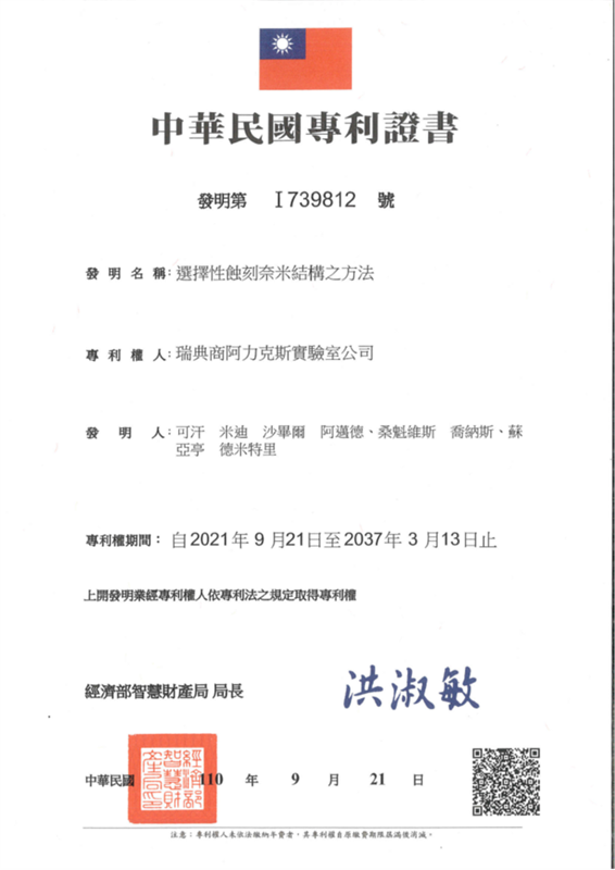
The Diploma to AlixLabs for the recently Granted Patent (TW I739812) in Taiwan issued by The Taiwan Intellectual Property Office (TIPO, 經濟部智慧財產局)

Dr. Mohammad Karimi, R&D and Operation Manager, added, "I am delighted that ALixLabs has been granted a 1 Million SEK project to verify the APS technology in the fabrication of FinFET and GAA-FET transistor architectures by Vinnova in June 2021".. Dr. Jonas Sundqvist, CEO and co-founder of AlixLabs, concluded that "The strategy as we advance is to successfully transfer the APS technology to 300 mm wafer processing in Dresden, Germany and making it readily available for process demonstration for the leading IDMs & Foundries. We don't only hope to cut cost in semiconductor manufacturing but also to reduce the energy and clean water demand and output of greenhouse gasses during chip manufacturing considerably. This is not by itself a Green Fab Technology. However, it takes one small step in the right direction."

* Atomic Layer Etch Pitch Splitting (APS). As previously reported (April 30, 2021), The US Patent Office has approved AlixLabs's patent application for nanofabrication by ALE Pitch Splitting (APS). The US Patent Office has issued a patent (US10930515) on February 23, 2021. The patent covers methods to split nanostructures in half by a single process step using Atomic Layer Etching (ALE). The method can have a significant impact on the semiconductor industry by enabling sustainable scaling of electronic components and shrink chip designs further in a cost-effective way. The method is complementary for single exposure Immersion and Extreme UV (EUV) Lithography and corresponding multiple patterning technologies like self-aligned double and quadruple patterning (SADP resp. SAQP) as well as multiple exposure lithography-etch and directed self-assembly (DSA).
** Wikipedia
*** September 15, 2021-Hsinchu News, SEMI (International Semiconductor Industry Association) https://www.semi.org/zh/world_fab_forecast_fabuctor Industry Association) https://www.semi.org/zh/world_fab_forecast_fab

Jonas Sundqvist, CEO of AlixLabs, phone +46 767 63 94 67, email jonas@alixlabs.com

AlixLabs (www.alixlab.com) is an innovative startup founded in 2019 in Lund, Sweden, enabling the semiconductor industry to scale down Logic and Memory components in a cost-effective manner by the use of ALE Pitch Splitting (APS).

Friday, October 8, 2021

Forge Nano Installs Prometheus™ Powder Atomic Layer Deposition (PALD) equipment at Air Liquide's Tokyo Innovation Campus

Forge Nano, a global leader in surface engineering with atomic layer deposition (ALD) sells the top-of-the-line Prometheus™ development system. Air Liquide is using the system to validate applications for ALD-enabled powders in Japan and Globally.

DENVER and YOKOSUKA, Japan, Oct. 1, 2021 /PRNewswire/ -- Forge Nano, a Denver-based advanced materials equipment company, has installed one of their flagship Prometheus™ powder ALD (PALD) systems at Air Liquide Japan Ltd.'s Tokyo Innovation Campus. The Prometheus™ research and development system is being used by Air Liquide to validate ALD precursor chemicals for PALD applications for a variety of applications including battery materials for electric vehicles and electronic materials for consumer devices. Air Liquide, an investor in Forge Nano, is using the Prometheus™ system to perform various proofs-of-concept for subsequent scale-up at customer facilities using Forge Nano's commercial scale equipment.


Forge Nano Prometheus ALD Tool. Atomic Layer Deposition Equipment

"Forge Nano values Air Liquide as a key strategic investor and partner in various established markets. We're excited to provide them with a research system to accelerate adoption of PALD technology in Japan and globally for new applications. Once proofs of concept are completed by Air Liquide, we will provide end customers with commercial scale PALD equipment," Dr. Daniel Higgs, Director Product Management.

"Forge Nano is a recognized leader in the development and industrialization of cutting-edge powder-ALD processes. As the global leading ALD precursors "designer" and supplier, we are excited to install a Prometheus PALD system to support our discovery and scale-up of new ALD applications, together with our worldwide customers and partners," Nicolas Blasco, Air Liquide Advanced Materials, Global Director, Emerging Markets.

Prometheus™ PALD system:
The Prometheus™ PALD system is Forge Nano's flagship R&D system for ALD on powders. It incorporates over 20 years of powder ALD know-how and was designed for ease of use, research flexibility, and quality of coatings. With advanced powder fluidization technology and up to 8 ALD chemical precursor lines, Prometheus™ is the most capable powder ALD system on the market.

Prometheus features:
  • 1mL – 600ml (~1kg) of powder per batch.
  • Proprietary fluidization technology enables uniform fluidization and deposition
  • Up to 8 ALD chemical precursors connection enable a multitude of coatings
  • Interchangeable reactor bodies ensure precise coating of various batch sizes
  • Inert isolation and handling capabilities of air-sensitive powders
Forge Nano's team of ALD experts guide our customers through the entire process, making ALD feasible for nearly any industry. Forge's commercial systems for ALD on powders include Lithos™, Circe™, Morpheus™, while their systems for ALD on wafers/objects include Theia™, Apollo™, and Helios™.

About Forge Nano:
Based in Denver, CO., Forge Nano is a global leader in surface engineering and precision nano-coating technology, using Atomic Layer Deposition. Forge Nano's proprietary technology and manufacturing processes make angstrom-thick coatings fast, affordable and commercially viable for a wide range of materials, applications and industries. Forge Nano's suite of ALD and PALD products and services cover the full spectrum from lab-scale tools to commercial-scale manufacturing systems.
For more information visit www.ForgeNano.com

About Air Liquide Advanced Materials:
A world leader in gases, technologies and services for Industry and Health, Air Liquide is present in 78 countries with approximately 64,500 employees and serves more than 3.8 million customers and patients. Air Liquide Advanced Materials (ALAM) is transforming the science of electronics and technology. We innovate with atomic scale engineering to open up countless new possibilities in how the world lives, works and connects. Today, our ALOHA™ and Voltaix® products are critical to the manufacture of the newest computer chips required for Big Data and the Internet of Things.

Wednesday, October 6, 2021

Nanexa receives orders for ALD coating of sensors for detection of nuclear detonations

Nanexa AB (www.nanexa.com) recently announced that the company has received two orders for a substantial number of sensors for detection of radioactive isotopes of the noble gas xenon, from two American customers, totaling approximately SEK 1.7 million. 

”The order are a strong confirmation of our unique competence within Atomic Layer Deposition (ALD), the core technology in our drug delivery system PharmaShell®. Although it is outside the scope of our core business, we are happy to continue to support our customers in this area”, said David Westberg, CEO of Nanexa. 

The sensors are key components in equipment developed for detection of nuclear detonations, even if they are carried out deep underground. Delivery of the coated sensors is expected during the autumn of 2021. The American customers consist of a leader in engineering and manufacturing of advanced technical systems for, among others, the defense and space industries, and a government laboratory.


Dutch deep tech start-up Delft IMP secures €10 million series A funding to scale up technology that radically extends battery life

Sandwater, a Nordic venture capitalist and Invest-NL have agreed to a €10 million investment in Delft IMP. This allows Delft IMP to accelerate their nanocoating process to industrial scale enabling more durable batteries and other sustainable applications. The investors in this Series A are Sandwater and Invest-NL. Sandwater has a broad portfolio of investments aiming to enable progress together with its founders. Invest-NL is the government owned impact investor supporting innovation and sustainability in the Netherlands. 


Delft IMP has unique expertise in developing ultra-thin coatings on powders and has the proprietary technology to produce these materials at scale. The ultra-thin nanocoatings protect, for example battery powder from the harsh surroundings and thus enhances the life time of the battery. The Delft IMP application technology enables them to control the process to optimize the film thickness and reduce the use of scarce raw materials. 

Ruud van Ommen

Founder & Professor in Chemical Engineering at TU Delft


Jacob Moulijn

Founder & Emeritus Professor in Catalysis Engineering at TU Delft

The real benefit of the Delft IMP technology comes from the elegant way they are able to scale up the atomic layer deposition (ALD) based coating process to industrial scale. This makes it possible to deliver this benefit cost effective to a wide range of battery applications, supporting the electrification of mobility. Coating the battery powders, provides the flexibility to encounter this benefit in current and also future generations. Delft IMP is not your next battery company, but instead they work together with leading battery companies to extend the lifetime of batteries and reduce the consumption of scarce minerals. This facilitates the sustainable use of raw materials, and will also bring radical performance improvements to other technologies such as electrolysers and fuel cells. 

“We are solving the big problems in the world, by going very small: We are applying ultra-thin coatings on powder material and enable production at scale with a unique technology originating from Delft University of Technology.” said Dr. Roderik Colen, CEO of Delft IMP. 

Torkel Engeness (Sandwater) “We at Sandwater are in the market for the radical solutions of tomorrow. Sandwater believes that active ownership enables progress and is looking forward to sharing the journey together with Invest NL and Delft IMP”.

Tuesday, October 5, 2021

Post Doc position in ALE and Steven M. George Lab, Boulder Colorado

Department of Chemistry, University of Colorado, Boulder, CO 80309 

We seek a highly-motivated individual for a postdoctoral position, available immediately, to join the laboratory of Prof. Steven George in the Department of Chemistry, at the University of Colorado in Boulder, CO. The successful candidate will conduct experiments on a quadrupole mass spectrometry molecular beam system designed for exploring reaction pathways in thermal atomic layer etching (ALE). 

A link to a recent publication showing research from this system can be found at the bottom of this posting. The successful candidate will operate as part of team, collaborating with researchers on other ALE experiments and with theoretical chemists. Additionally, the successful candidate should have experience with vacuum hardware, a strong track record of research, and capable interpersonal skills. A Ph.D. in chemistry or a related field (materials science, engineering, or physics) is required. 


Jonathan Partridge and Ann Lii-Rosales exchanging substrates on a quadrupole mass spectrometry molecular beam ALE system.

At the foot of the Rocky Mountains, Boulder, CO is known for its scenic beauty, high quality of life, and active lifestyles. 

For more information about the George Research Group please see:


Please send a cover letter, CV and the names of two references to Prof. Steven George at
Steven.George@Colorado.edu
.

Call for Abstracts - 6th Area Selective Deposition Workshop (ASD 2022)


Call for Abstracts, Due February 7, 2022

An effort to help facilitate the progression of ASD techniques, the 6th Area Selective Deposition Workshop (ASD 2022) scheduled for April 21-22, 2022, in San Francisco will act as a central event for sharing and discussing the newest developments in ASD by gathering leading experts from both academia and industry. Attendees can expect to participate in talks regarding fundamental challenges related to recent developments in ASD, applications for ASD in next-generation technology, emergent processes for implementing ASD techniques, and new perspectives on metrological and characterization strategies for further understanding persistent mechanistic challenges. Based on the success of the previous workshops, ASD 2022 will consist of two days of presentations by invited and contributing speakers, as well as a banquet reception and poster session.

Topics:

This event is centered on showcasing developments across the whole spectrum of area-selective deposition. Thus, the Workshop will cover a wide range of topics including the following:

· Near Term Technology Readiness (Scalable and Relevant ASD Processes for Use in Manufacturing)
· Fundamentals of ASD (Defects, Growth Mechanisms and Inhibitor Chemistries)
· Metrology Techniques for ASD
· Emerging/Exploratory ASD Processes and Applications (e.g., Catalysis, Energy Generation and Storage)


Key Deadlines:

Call for Abstracts Deadline: February 7, 2022
Author Acceptance Notifications: February 21, 2022
Hotel Reservation Deadline: March 4, 2022
Early Registration Deadline: March 4, 2022


Program Chair:

Rudy J. Wojtecki
IBM Almaden Research Center, USA
Questions? Contact rjwojtec@us.ibm.com


The dynamics in CVD and PEALD of InN

Epitaxial nanometer-thin indium nitride (InN) films are considered promising active layers in various device applications but remain challenging to deposit. Pedersen's group at Linköping University, Sweden, has compared the morphological evolution and characterizations of InN films with various growth conditions in CVD by both a plasma ALD approach and a conventional metalorganic CVD approach. 

Their results show that a time-resolved precursor supply is highly beneficial for deposition of smooth and continuous InN nanometer-thin films. The time for purging the reactor between the precursor pulses and low deposition temperature are key factors to achieve homogeneous InN. The gas exchange dynamics of the reactor is further studied using computational fluid dynamics. 


Top-view SEM images of InN grown on SiC by using both ALD and continuous CVD at different deposition temperatures: (a) 320, (b) 400, and (c) 450 °C. In each figure, the result from ALD is shown in the upper right part while the result from continuous CVD is shown in the bottom left part. (Journal of Applied Physics 130, 135302 (2021); https://doi.org/10.1063/5.0061926)

A Picosun R-200 ALD system was employed to grow InN films using trimethyl indium, In(CH3)3 (TMI), and plasma discharged NH3/Ar gas mixture and an Aixtron/Epigress horizontal hot-wall MOCVD reactor was used to grow InN for comparison.


X-ray diffractograms of (a) symmetric 2θ-ω scan of InN films deposited on 4H-SiC (0001) by ALD and continuous CVD. The process temperatures of ALD are indicated, respectively, in the plot. The curves are plotted in the log scale and are shifted vertically for visual clarity. (b) ω scan of InN (0002) and SiC (0004) of samples deposited at different temperatures.

According to their study, 320 °C is found to be the upper temperature where the dynamics of the deposition chemistry can be controlled to involve only surface reactions with surface species. The results highlight the promising role of the ALD technique in realizing electronic devices based on nanometer-thin InN layers.

This study and previous findings in the literature demonstrate the importance of using a time-resolved precursor supply in CVD of InN in which the purge time plays an important role. It should also be noted that the best results in this study are outside the window where the deposition per ALD cycle is constant in temperature. Such observation suggests that a true, self-limiting ALD behavior is not the most critical factor but rather the dynamic precursor supply. Meanwhile, the experimentally optimal purge time and precursor pulse time should vary from reactor to reactor based on their geometry and volume.

Reference: On the dynamics in chemical vapor deposition of InN, Journal of Applied Physics 130, 135302 (2021); https://doi.org/10.1063/5.0061926

Sunday, October 3, 2021

Call for Research ArticlesSpecial Topic Collections:Atomic Layer Deposition and Atomic Layer Etching

Call for Research Articles
Special Topic Collections:
Atomic Layer Deposition and Atomic Layer Etching
Manuscript Deadline: November 15, 2021

The Journal of Vacuum Science and Technology A is soliciting research articles for publication in Special Topic Collections on Atomic Layer Deposition and Atomic Layer Etching. These special topic collections are planned in collaboration with the annual ALD meeting and ALE Workshop.

Each year, in concert with the annual Atomic Layer Deposition (ALD) meeting and Atomic Layer Etching (ALE) Workshop, the Journal of Vacuum Science and Technology A publishes collections of articles covering the most recent developments and experimental studies in ALD and ALE. These ALD and ALE Special Topic Collections will include papers presented at the annual meeting and Workshop, as well as other ALD and ALE research articles that were not presented at the conference but are submitted to the collections. The collections feature articles dedicated to the science and technology of atomic layer controlled deposition and etching.


Authors are encouraged to use the JVST article template. During submission, you will have an opportunity to tell us that your paper is a part of one of the Collections by choosing either the Special Topic or Conference Collection on “Atomic Layer Deposition (ALD)” or “Atomic Layer Etching (ALE).” See recent collections: ALD 2021, ALE 2021, ALD 2020, and ALE 2020.

Saturday, October 2, 2021

ASM International Investor Day take away - the leader in ALD wafer processing equipment for the booming semiconductor industry

 ASM International, the leader in ALD wafer processing equipment for the booming semiconductor industry recently hold its annual investor day.

Highlights included:
  • Targeting revenue of €2.8-€3.4 billion by 2025 (2020-2025 CAGR of 16%-21%), gross margins of 46%-50% in 2021-2025, and operating margins of 26%-31% in 2021-2025;
  • Targeting Net Zero emissions by 2035 and 100% renewable electricity by 2024;1
  • Single-wafer ALD market expected to increase from $1.5 billion in 2020 to $3.1-3.7 billion by 2025;
  • Further capacity expansion of our new manufacturing facility to be production ready by early 2023.

3D device architecture evolution is continuing into all leading-edge semiconductor components. 3DNAND and FinFET are to be followed by GAA FETs and 3D-DRAM. Together with the need for new materials drives the demand for CVD and ALD processing equipment (ASM Investor Day 2021)

“I’m very excited to share the strong prospects for our company during our first Investor Day,” said Benjamin Loh, CEO of ASM International. “We project revenue to increase to €2.8–€3.4 billion by 2025, with operating margins of 26%-31% during the 2021-2025 period. Key inflections in next generation semiconductor devices such as complex 3D architectures and new materials, are expected to drive double digit growth in ASM’s key markets. Today we will also highlight new innovations in our products, enabling our customers’ technology roadmaps. Capitalizing on our innovative strength, early customer engagements and product differentiation, we are focused on maintaining our leading position in the ALD market and to further increase our market share in Epi.


The semiconductor market, historical and as forecasted by VLSI Research. By 2030 it will have doubled to USD 1 Trillion. (VLSI Research - ASM Investor Day 2021)

In view of the strong growth opportunities ahead of us we will further step up our R&D investments and strengthen our capabilities. In addition, with our new expanded manufacturing facility in Singapore completed just less than one year ago, we have now decided to prepare a further substantial capacity increase within this facility to be production ready by early 2023.


The Wafer Equipment market growth has reached a new level and will sustain it for years to come (VLSI Research - ASM Investor Day 2021).


ASM controls more than 50% of the single wafer ALD equipment market and intends to defend the market share going forward to 2025. The market is forecasted by ASM to more than double 2020 to 2025, reaching USD 3.1 to 3.7 billion by then. (ASM Investor Day 2021)

A further increase in our ambition to sustainability is a central element in our strategy. As an important next step we announce today our ambitious target to achieve Net Zero emissions by 2035 (scope 1, 2 and 3) and 100% renewable electricity by 2024. As we continue to drive growth through innovation, ASM is well positioned to create long-term value for all its stakeholders.”


ASM Roadmap for DRAM, 3D-NAND and Logic,  aligned with its leading-edge customer base. (ASM Investor Day 2021)

The Investor Day was held at 2:00 pm CET  and Q&A can also be followed through a live webcast after registering at: https://investorday.asm.com.

Presentation:LINK

UPDATE Q3 2021 GUIDANCE

ASM also announced that Q3 order intake is expected to be above €600 million, compared to previous guidance of €510-530 million, mainly driven by continued strong demand in the logic/foundry sector. Q3 net sales are expected to be in line with previous guidance €400-430 million.

Swedish Semiconductor Startup AlixLabs Raises USD 1 Million Seed Capital

TUE, SEP 28, 2021 00:01 CET, Almi Invest is investing close to SEK 3 million in AlixLabs, which is developing a new method for manufacturing semiconductor components cheaper and faster. Private investors, including NHL professionals Michael, Alexander and William Nylander, are also participating in the issue for a total of SEK 9 million (USD 1 million). The funds will be used for product development and validation of the APS-technology.

Semiconductor components build up the computer chips found in virtually all electronic products, such as smartphones, servers, game consoles, computers and cars. They can be described as the brain and memory that make electronic products work.Today's semiconductor components are extremely small, making them more difficult and expensive to manufacture. The industry is working to cope with this challenge through new and innovative approaches. Common to these new methods is that they are complex and in most cases extremely expensive.

Now AlixLabs from Lund, Sweden, has developed a new, innovative method for manufacturing semiconductor components with a high degree of packing, which eliminates several steps in the manufacturing process - Atomic Layer Etch Pitchsplitting (APS)*. The method makes the components cheaper and less resource-intensive to manufacture and can open up a new path for a more sustainable mass production of electronics. The method also makes it possible to manufacture extremely small semiconductor components in an accurate and efficient way, which means that also smaller production facilities in, for example, Europe will be able to manufacture the components with manageable investments. Today, basically all production of leading edge semiconductors takes place in the USA and Asia, mainly in Taiwan and South Korea.


Dr. Jonas Sundqvist, CEO of AlixLabs AB.

- AlixLab's disruptive manufacturing method has enormous market potential and enables continued technology development and more powerful electronics that are at the same time much more resource-efficient, says Anna Gisselsson, Investment Manager at Almi Invest.The company's method is covered by an approved patent in the United States* and it has additional patent applications in other countries.

- Thanks to this investment, we can take the company to the next level, says Dr. Jonas Sundqvist, CEO of AlixLabs. Today, we have a number of ongoing negotiations with R&D actors, equipment and semiconductor manufacturers to create a basis for further cooperation for the development of our products. In the longer term, we want to create an ecosystem covering the complete value chain for APS and we hope to have a strong base in Europe with a global reach.

.- The R&D from these funds will allow us to strenghten and expand our IP portfolio for our properitary APS-technology, says Dr. Dmitry Suyatin, CTO of AlixLabs.


From left to right, Dr. Dmitry Suyatin, CEO, Dr. Mohammad Karimi R&D and Operations Manager, and Dr. Jonas Sundqvist, CEO.


AlixLabs Board of directors: https://www.alixlabs.com/who-we-are

* Atomic Layer Etch Pitch Splitting (APS). As previously reported (April 30th, 2021) The US Patent Office has approved AlixLabs’s patent application for nanofabrication by ALE Pitch Splitting (APS). The US Patent Office has issued a patent (US10930515) on February 23, 2021. The patent covers methods to split nanostructures in half by a single process step using Atomic Layer Etching (ALE). The method has the potential to have a big impact on the semiconductor industry by enabling sustainable scaling of electronic components and shrink chip designs further in a cost-effective way. The method is complementary for single exposure Immersion and Extreme UV (EUV) Lithography and corresponding multiple patterning technologies like self-aligned double and quadruple patterning (SADP resp. SAQP) as well as multiple exposure lithography-etch and directed self-assembly (DSA).

Jonas Sundqvist, CEO of AlixLabs, phone +46 767 63 94 67, email jonas@alixlabs.com

AlixLabs (www.alixlab.com) is an innovative startup founded in 2019 in Lund, Sweden, enabling the semiconductor industry to scale down Logic and Memory components in a cost-effective manner by the use of ALE Pitch Splitting (APS).

Thursday, September 30, 2021

ALD is everywhere - Take us it away, Picosun, born in Finland, born to ALD

ALD as a technology is not widely known to every man on the street. However, a new video shows how we are surrounded by it in our everyday lives.

Take us it away - Picosun, born in Finland, born to ALD


ALD Stories Ep 6 - ALD Precursor Design for Hard to Deposit Metals with Prof. Chuck Winter

Tyler sits down with Wayne State University’s Chuck Winter to talk about his approach to designing precursors for ALD. Chuck explains what makes a good ALD precursor and how elegant organic chemistry can enable ALD processes for hard-to-deposit metals, like cobalt and aluminum. 

Learn more about Chuck’s research here: http://www.clas.wayne.edu/wintergroup/ 

Papers mentioned in this episode: 


Selectivity Enhancement for Ruthenium Atomic Layer Deposition in Sub-50 nm Nanopatterns by Diffusion and Size-Dependent Reactivity

Area-selective deposition (ASD) is a promising bottom-up approach for fabricating nanoelectronic devices. The challenge is to prevent the undesired growth of nanoparticles in the nongrowth area. 

In this work from Belgium and The Netherlands research teams, linewidths of 50 nm and smaller, all Ru adspecies are captured at the growth interface before growth by precursor adsorption is catalyzed. This is more than 1000 times lower than for patterns with a linewidth of 200 nm and larger, where the Ru content decreases significantly only near the interface with the growth surface. 

The predicted depletion zone is confirmed by experiments in nanoscale line-space patterns. Overall, this mechanism results in smaller and fewer Ru nanoparticles for smaller patterns, facilitating the development of passivation-deposition-etch ASD processes for nanoelectronic device fabrication.

Selectivity Enhancement for Ruthenium Atomic Layer Deposition in Sub-50 nm Nanopatterns by Diffusion and Size-Dependent Reactivity

Jan-Willem J. Clerix, Esteban A. Marques, Job Soethoudt, Fabio Grillo, Geoffrey Pourtois, J. Ruud Van Ommen, Annelies Delabie,
3 September 2021


Area-selective deposition (ASD) is a promising bottom-up approach for fabricating nanoelectronic devices. However, a challenge is to prevent the undesired growth of nanoparticles in the nongrowth area. This work uses kinetic Monte Carlo (KMC) methods to investigate the defectivity in ruthenium ASD by (ethylbenzyl)(1-ethyl-1,4-cyclohexadienyl)Ru/O2 (EBECHRu) atomic layer deposition (ALD) in line-space nanopatterns with different dimensions. Ru ASD is governed by adsorption as well as diffusion. The defectivity depends on the pattern dimensions, as nanoparticles can diffuse and reach the interface with the growth area where they aggregate. For linewidths of 50 nm and smaller, all Ru adspecies are captured at the growth interface before growth by precursor adsorption is catalyzed. The synergetic effect of diffusion and size-dependent reactivity reduces defectivity below 1010 Ru atoms cm−2 for at least 1000 ALD cycles. This is more than 1000 times lower than for patterns with a linewidth of 200 nm and larger, where the Ru content decreases significantly only near the interface with the growth surface. The predicted depletion zone is confirmed by experiments in nanoscale line-space patterns. Overall, this mechanism results in smaller and fewer Ru nanoparticles for smaller patterns, facilitating the development of passivation-deposition-etch ASD processes for nanoelectronic device fabrication.


Wednesday, September 29, 2021

Status & Challenges in Today's Atomic Layer Processing Market J. Sundqvist (Keynote TECHCET LLC CA)

ALD at ECS is coming up and it is for free! Besides all the interesting sessions on ALD there is one on ALD Present and Future. I look forward to meet you there in Florida and give one of the Keynotes on Status & Challenges in Today's Atomic Layer Processing Market followed by much more interesting talks by Stacy Bent (Stanford University) and Mattia Pasquali (Imec)


Monday, 11 October 2021


Sunday, September 19, 2021

1 min introduction of Han Bo Ram Lee Lab (HBRLRG, Korean version)

Even if you do not speak Korean you can understand almost everything in this amazing video from Han-Bo-Ram Lee lab - stay tuned for the English version!


ALD can improve surgical tools like scalpel blades and much more

A recent article published in MDPI (LINK) discusses a study where zinc oxide thin film was deposited on surgical knife blades with ALD. The study shows that surgical instruments coated with non-allergenic metal oxide coatings containing metal structures that reduce the growth of bacteria could significantly decrease the risk of undesirable reactions of the body during and after surgery.


"The use of ALD methods in medicine allows us to enter a completely new generation of in vivo medicine. The ALD method makes it possible to meet the high requirements regarding mechanical and anti-corrosion properties, chemical and thermal resistance, as well as biocompatibility for tools used in medicine."

Here ALD coatings performed in a Picosun R 200 System have been investigated by Polish researchers.

Application of ALD Thin Films on the Surface of the Surgical Scalpel Blade

1
Department of Engineering Materials and Biomaterials, Silesian University of Technology, Konarskiego 18a Str., 44-100 Gliwice, Poland
2
Scientific and Didactic Laboratory of Nanotechnology and Material Technologies, Faculty of Mechanical Engineering, Silesian University of Technology, Towarowa 7 Str., 44-100 Gliwice, Poland
3
Faculty of Biomedical Engineering, Silesian University of Technology, Roosevelta 40, 41-800 Zabrze, Poland
*
Author to whom correspondence should be addressed.
Academic Editor: Angela De Bonis
Coatings 202111(9), 1096; https://doi.org/10.3390/coatings11091096
Received: 11 August 2021 / Revised: 3 September 2021 / Accepted: 7 September 2021 / Published: 11 September 2021


Saturday, September 18, 2021

University of Helsinki presents Self-Aligned Thin-Film Patterning by Area-Selective Etching of Polymers

A promising path to cut cost, scale, and reduce the environmental impact of semiconductor manufacturing

One of the driving costs in the high volume production of semiconductor components for especially powerful processors and memory chips is the patterning process. Both the capital investment in photolithographic equipment and the design cost add to the escalating cost going down to smaller nodes (see figure below). If one can reduce the number of lithographic mask layers needed in the production for a chip design one automatically cut the overall cost. Another problem is that while scaling down designs to smaller critical dimensions and tighter pitches and scaling up in the 3rd dimension like for 3D-NAND and coming 3D-DRAM it becomes more difficult to match the next mask layer with the previous one. The industry has solved this issue successfully for many years by introducing self-aligned processes like self-aligned contacts to the source, drain, and gate of the transistors below. Also, selective deposition processes like selective Epi and Cobalt CVD caps on copper are in production.

From an environmental view, lithography and mask more mask layers also consume more energy and clean water. Recent reports from Taiwan have it that both are problems, where drought has led to water shortages and the overall energy demand from fabs are high (about 5% of Taiwan total demand in 2019). 

Here, the University of Helsinki presents a process sequence for the future that is self-aligned and selective making it possible to mitigate all those problems in a very clever way for future devices and metallization schemes - please find all the details in the article below that is open source for download.

Self-Aligned Thin-Film Patterning by Area-Selective Etching of Polymers

by Chao Zhang, Markku Leskelä and Mikko Ritala *

Coatings 2021, 11(9), 1124; https://doi.org/10.3390/coatings11091124

Patterning of thin films with lithography techniques for making semiconductor devices has been facing increasing difficulties with feature sizes shrinking to the sub-10 nm range, and alternatives have been actively sought from area-selective thin film deposition processes. Here, an entirely new method is introduced to self-aligned thin-film patterning: area-selective gas-phase etching of polymers. The etching reactions are selective to the materials underneath the polymers. Either O2 or H2 can be used as an etchant gas. After diffusing through the polymer film to the catalytic surfaces, the etchant gas molecules are dissociated into their respective atoms, which then readily react with the polymer, etching it away. On noncatalytic surfaces, the polymer film remains. For example, polyimide and poly(methyl methacrylate) (PMMA) were selectively oxidatively removed at 300 °C from Pt and Ru, while on SiO2 they stayed. CeO2 also showed a clear catalytic effect for the oxidative removal of PMMA. In H2, the most active surfaces catalysing the hydrogenolysis of PMMA were Cu and Ti. The area-selective etching of polyimide from Pt was followed by area-selective atomic layer deposition of iridium using the patterned polymer as a growth-inhibiting layer on SiO2, eventually resulting in dual side-by-side self-aligned formation of metal-on-metal and insulator (polymer)-on-insulator. This demonstrates that when innovatively combined with area-selective thin film deposition and, for example, lift-off patterning processes, self-aligned etching processes will open entirely new possibilities for the fabrication of the most advanced and challenging semiconductor devices.


Schematics showing self-aligned polymer etching and the subsequent film patterning through area-selective deposition and lift-off processes. (Zhang et al Coatings 2021, 11(9), 1124, figure 1)

This is an open access article distributed under the Creative Commons Attribution License which permits unrestricted use, distribution, and reproduction in any medium, provided the original work is properly cited

Semiconductor design and manufacturing: Achieving leading-edge capabilities, McKinsey LINK

Wednesday, September 15, 2021

Problem solved - In0.5Ga0.5N layers by Atomic Layer Deposition!

Pedersen Group at Linköping University, Sweden, present an ALD approach to metastable In1-xGaxN with 0.1 < x < 0.5 based on solid In- and Ga-precursors that were co-sublimed into the deposition chamber in one pulse. A near In0.5Ga0.5N film with a bandgap of 1.94 eV was achieved on Si (100) substrate. Epitaxial In1-xGaxN (0002) was successfully grown directly on 4H-SiC (0001).

In0.5Ga0.5N layers by Atomic Layer Deposition
P. Rouf, J. Palisaitis, B. Bakhit, N. J. O'Brien and H. Pedersen, J. Mater. Chem. C, 2021, DOI: 10.1039/D1TC02408F. (LINK)


a) Cross-sectional STEM-HAADF image of the ~60 nm In1-xGaxN film on 4H-SiC substrate with a zoomed in image of the b) In82Ga18N and c) In18Ga82N layers. d) SAED pattern from the film and substrate. EDX maps of Ga e), In f) and Si g). EELS maps of N h) and C i).

Tuesday, September 7, 2021

Picosun Innovation Lab, opened in September 2021

Picosun Innovation Lab, opened in September 2021, will be used for the company’s own research and development projects, for demo purposes and most importantly for serving the company’s global semiconductor customers operating in the 300 mm market.


ESPOO, Finland, 7th of September 2021 – Picosun Group has taken into use new facilities at its production laboratory in Kirkkonummi, Finland. The Picosun Innovation Lab will be used for the company’s own research and development projects, for demo purposes and most importantly for serving the company’s global semiconductor customers operating in the 300 mm market.

The Innovation Lab hosts Picosun’s new generation tools PICOSUN® Morpher and PICOSUN® Sprinter. Morpher was launched in 2019 and it started a completely new era in Picosun products. Its adaptive and versatile nature makes it an ideal ALD solution for to the changing needs of different business verticals in the up to 200 mm wafer industries. Sprinter was launched late 2020 for the 300 mm wafer markets to meet the ever-increasing demands of semiconductor, display and IoT component manufacturing lines. It has brought single wafer film quality and uniformity for fast batch processing and met the challenges in high volume ALD manufacturing.

The Innovation Lab increases the laboratory capacity Picosun currently has on its premises significantly. The new facilities will have the ability to host tens of ALD tool modules. The facilities also support a variety of process gases including for example N2, O2, O3, Ar, H2, NH3 and NF3. Furthermore, special attention has also been paid for the best-in-class building management and safety systems.

“The opening of the new Innovation Lab reflects our role in being the pioneer in ALD and continuing the daily work in setting the standards for future innovations in the ALD sphere. The Innovation Lab has been a big investment for the company, but we see this as an essential investment to our and our customers’ future”, says Jussi Rautee, CEO of Picosun Group.

Friday, September 3, 2021

The world’s largest ALD system - The BENEQ P1500 is here!

Now it is here - The Beneq P1500 is the biggest ALD system and is built specifically to coat sizeable sheets and complex parts. It is also made to deliver increased throughput for batches of smaller components.


Beneqs customers use the P1500 for optical coatings on large diameter substrates, anticorrosive coatings of semiconductor equipment parts, and various applications where ALD is used on glass or metal sheets.


Large parts need large ALD tools. The Beneq P1500 can accommodate parts up to 1300 × 2400 mm in size, and enables the deposition of high-quality, functional optical coatings on wide area mirrors or lenses. It is also used to coat batches of parts in the 300 to 1000 mm size range.

More information: LINK


Wednesday, September 1, 2021

Picosun strengthens its position in the semiconductor market

ESPOO, Finland, 31st of August 2021 – Picosun Group strengthens its position in the 300 mm semiconductor market with its new generation ALD tool PICOSUN® Sprinter.


PICOSUN® Sprinter was first launched in December 2020 as a stand-alone module. Now also customer deliveries and installations of PICOSUN® Sprinter clusters have started.

“A Sprinter cluster consist of two Sprinter modules and a central vacuum wafer-handling robot utilizing 5-wafer handling. The set-up enables a throughput of more than 100 wafers an hour with 10 nm aluminium oxide target film thickness”, explains Juhana Kostamo, VP, Industrial Business Area of Picosun Group.

“The throughput capability combined with the unique design of the tool’s reaction chamber, the record-breaking batch film quality and the fact that the tool can be fully integrated with the customers’ production line, makes PICOSUN® Sprinter the tool of choice for semiconductor, display and IoT component industries who need a future-proof tool with single wafer film quality and uniformity in fast batch processing”, Kostamo concludes.